Article

Morphological and Doping Effects on Electrical Conductivity of Aluminum Metal Substrate through Pulsed Electrodeposition Coating of Cu-MWCNT

by
Alberto S. Silva
1,2,*,
Mário E. S. Sousa
1,2,
Eduardo M. Braga
3 and
Marcos A. L. Reis
1,2,3
1
Postgraduate Program in Materials Science and Engineering, Federal University of Pará, Ananindeua Campus, Ananindeua 67130-660, Brazil
2
3D Nanostructuring Laboratory, Federal University of Pará, Guamá Campus, Belém 66075-110, Brazil
3
Postgraduate Program in Natural Resources Engineering of the Amazon, Institute of Technology, Federal University of Pará, Guamá Campus, Belém 66075-110, Brazil
*
Author to whom correspondence should be addressed.
Metals 2024, 14(9), 1060; https://doi.org/10.3390/met14091060
Submission received: 11 August 2024 / Revised: 5 September 2024 / Accepted: 13 September 2024 / Published: 17 September 2024

Abstract

:
The demand for more efficient and sustainable electrical systems has driven research in the quest for innovative materials that enhance the properties of electrical conductors. This study investigated the influence of copper (Cu) coating and multi-walled carbon nanotubes (MWCNTs) on aluminum metal substrate through the pulsed electrodeposition technique. Parameters such as the concentration of chemical elements, current, voltage, temperature, time, and electrode spacing were optimized in search of improving the nanocomposite coating. The metallic substrate underwent anodization as surface preparation for coating. Characterization techniques employed included Field Emission Gun—Scanning Electron Microscopy (FEG-SEM) for analyzing coating morphology, Energy-Dispersive X-Ray Spectroscopy (EDS), Raman spectroscopy, and Kelvin probe for obtaining surface electrical conductivity values. Homogeneous dispersion of the Cu-MWCNTs film coating was achieved across the entire surface of the aluminum plate, creating a complex morphology. The doping effect was highlighted by changes in the vibrational characteristics of the nanocomposite, which affected the Raman spectrum dispersion bands. An increase in surface electrical conductivity by ≈52.33% compared to the control sample was obtained. Therefore, these results indicate that the improvement in the material’s electrical properties is intrinsically related to the complex morphology achieved with the adopted Cu-MWCNT nanocomposite coating process.

1. Introduction

There is a growing demand for materials that exhibit specific and enhanced electrical characteristics, such as low resistivity, high conductivity, and elevated electrical capacity, especially in the energy and electronics industry. Carbon nanotubes (CNTs)/Cu composites have attracted researchers’ attention due to their high electrical conductivity [1]. Furthermore, the development of composite materials combining CNTs with Cu on aluminum substrate has sparked significant interest in the scientific and technological community. The search for new materials with superior characteristics is driven by the need to develop more efficient and innovative technologies in various sectors, including electronics, energy, transportation, and communications. This combination offers a unique opportunity to develop composite materials with superior electrical conductivity properties, which can be applied in a wide range of devices and systems requiring high energy efficiency and electrical performance.
Studies have demonstrated that CNTs possess an estimated strengthening capability when incorporated on pure aluminum, resulting in composites that exhibit superior properties to conventional metallic materials [2]. CNTs possess unique properties; they have a density of 1.3 g/cm3 for single-walled carbon nanotubes (SWCNTs) and 2.1 g/cm3 for MWCNTs, both of which are much lower than that of copper, 8.96 g/cm3. They exhibit good environmental stability, being able to withstand severe conditions of high pressure and large temperature changes. Additionally, they possess excellent mechanical performance, with a Young’s modulus and tensile strength in the range of 1.0 TPa and 50 GPa, respectively, high electrical conductivity for SWCNTs of ≈108 S/m [3], and thermal conductivities from 2000 to 7500 W/mK [4]. When deposited as coating on the aluminum, they can form conductive networks, facilitating electron flow and enhancing electrical conduction efficiency. Furthermore, Cu is widely recognized for its excellent electrical conductivity, making it one of the most commonly used materials in applications requiring high efficiency in electrical conduction. The electrical conductivity of Cu is approximately 5.96 × 10⁷ S/m at room temperature, making it one of the most conductive metals. On the other hand, aluminum has been widely explored as a substrate in advanced studies due to its lightweight nature, high ductility, and malleability. It has been particularly highlighted in the field of power transmission networks due to its resistance to deformation and significantly lower weight compared to copper. Based on this premise, the main objective of this study was to employ the pulsed current electrodeposition technique to coat aluminum with MWCNTs and Cu. Thus, the main innovation of this work is to use the pulsed electrodeposition technique to coat an anodized aluminum metal substrate with Cu-MWCNTs in order to improve the electrical conductivity of the material.
Aluminum anodization is an electrochemical process that creates a layer of aluminum oxide (Al2O3) on the metal surface. This oxide coating is corrosion-resistant and adheres well to paints and coatings, making it an effective preparation for the application of additional coatings like MWCNTs. During the anodization process, porous membranes can be generated, resulting in the formation of an alumina layer with pores through anodic oxidation. These pores, in turn, offer the opportunity to be filled through the electrodeposition process. The use of pulsed direct current for cathodic electrophoretic deposition (pulsed-CEPD) was studied as a sealing technique for anodized AA2024 by depositing hybrid sol–gel films from aqueous suspensions [4]. Anodization treatments were used to etch the surface of the Al substrate with carbon fiber-reinforced plastic (CFRP) panels. CNTs were employed to enhance the bonding interfaces and adhesive layers [5]. In another study, anodized aluminum oxides (AAOs) were coated with CNTs and gold nanoparticles to be used as supports in a catalyst [6].
The use of the pulsed current electrodeposition technique, due to its numerous benefits in relation to the structure and properties of coatings, has been employed to obtain nanostructured coatings in research related to the development of new materials. Self-supporting 3D nanotwinned copper (Nt-Cu) structures were additively manufactured using pulsed electrodeposition at the tip of an electrolyte-containing nozzle, demonstrating the localized pulsed electrodeposition process in an ambient environment for direct printing of three-dimensional (3D) copper nanostructures [7]. FePt nanowires, which utilize one-dimensional magnetic nanotechnology and are known for their high biocompatibility and chemical inertness, were fabricated through pulsed electrodeposition in nanoporous aluminum oxide templates [8]. Cu-Al2O3 nanocomposites were produced via jet electrodeposition using pulsed current, aiming to improve both the deposition quality and its mechanical properties. The composite coatings obtained with pulsed current demonstrated a more uniform surface morphology, denser microstructure, and better mechanical properties compared to those obtained under direct current. Additionally, the impact of pulse parameters such as current density and frequency on the morphological, microstructural, grain growth, and coating properties was investigated. The results indicate that a high pulse frequency and appropriate current density contributed to enhancing both the deposition quality and its mechanical properties. The hardness of the coating reaches the peak at 623 HV [9]. Pulsed electrochemical deposition of thin aluminum films onto copper-coated printed circuit boards, using ionic liquids containing aluminum chloride and trimethylphenylammonium chloride, was investigated. As a result, it was observed that this technique provided thinner and more compact aluminum deposits compared to those obtained by conventional methods of electrochemical deposition using constant current [10].
The coating of functionalized copper/carbon (Cu/f-CNT) on 1350 aluminum alloy was performed through the electrophoretic deposition process using a copper sulfate and iodine solution, with an electric current of 1.2 A and a voltage of 10 V. At room temperature, the doping influence, combined with the remarkable properties of CNTs, resulted in an approximately 18% increase in the electrical conductivity of the nanostructured wire compared to the conventional wire, facilitating charge transfer and the creation of new metallic conduction channels [11]. Similarly, the electrodeposition process was used for the deposition of a copper-based MWCNT nanocomposite coating on 6061 aluminum to enhance its electrical and thermal properties. It was found that the incorporation of MWCNTs into the copper coatings increased electrical conductivity by 59.63%, 103.67%, and 128.44% for different MWCNT concentrations in the electrodeposition process compared to uncoated 6061 aluminum substrates [12].
From another point of view, a uniform dispersion of CNTs in a copper matrix was achieved by manufacturing self-supporting CNTs/Cu nanocomposite wires developed with electrical conductivity σ ≈ 5.5 × 10⁵ S cm−1 and ampacity of A ≈ 20 × 105 and 4 × 105 cm−2 for 1.5 and 17 mm gauge length wires, respectively, which is greater than those of copper [13].

2. Materials and Methods

Procedures were conducted to obtain the coating of copper and multi-walled carbon nanotubes (Cu-MWCNTs) through the pulsed electrodeposition technique on 3003 aluminum alloy sheets. These alloys not only possess good electrical conductivity, approximately 16.7 × 10⁶ S/m, but also exhibit excellent workability and corrosion resistance, facilitating surface preparation and treatment before the deposition of coatings. Table 1 describes the chemical composition limit data for aluminum alloy 3003. The anodization technique was utilized as a preparation step for the coating, creating a nanoporous alumina layer with the objective of improving the adhesion and structure of the coating with the nanocomposite.

2.1. Preparation, Cleaning and Conditioning

During the sample preparation procedure, three replicates were produced for analysis and comparison purposes to assess the impacts of the variations in experimental parameters. The objective was to optimize the electrodeposition method and enhance the effectiveness of the resulting coating. The replicas consisted of aluminum sheets with dimensions of 3 × 4 cm2, a thickness of 1 mm, and approximately 1.20 g of mass. To clean the surface of the samples, the following sequence was followed: cleaning with neutral liquid detergent and sponge; immersion in sodium hydroxide (NaOH) for five minutes with a concentration of 70 g/L; rinsing with demineralized water; immersion in hydrochloric acid (HCl) for 5 min; rinsing with demineralized water; drying in an oven for one hour at 50 °C; and packaging.

2.2. Anodization Process

A microprocessed square wave pulsating rectifier, the WG V® model (WG retificadores, Rio de Janeiro, RJ, Brazil), was employed as the power source during the anodization process. This equipment operates providing a maximum output voltage of 12 VDC, with adjustable frequency, current, and pulse capabilities. For the anodization cell, two copper plates served as counter-electrodes connected to the negative pole of the pulsed current source, while the aluminum substrate was configured as the working electrode (anode), connected to the positive pole of the source. The electrodes and the substrate were immersed in sulfuric acid (H2SO4) in a beaker, with a concentration of 100% and a molecular weight of 98.08 g/mol. In Stage 1, a voltage of 10 V and a pulsed current of 3 A with a duty cycle of 80% were applied for 30 min in a temperature range of 28 °C to 30 °C during the anodizing process. For Stages 2 and 3, the parameters were modified using a voltage of 10 V and a direct current (DC) of 3A for 120 min. Oxygen was not supplied separately during the anodization process. To minimize oxygen concentration polarization, which can affect the uniformity of the anodic layer, the experiments were conducted in a fume hood; temperature control was employed along with agitation of the solution using an ultrasonic bath ensuring a more uniform formation of the anodic layer.

2.3. Coating of Cu-MWCNTs Using the Pulsed Electrodeposition Process

After the anodization of the aluminum plates, the Cu-MWCNTs electrodeposition step was performed. Thus, the preparation of the electrolytic solution was carried out following the next steps: mixing of pentahydrated copper sulfate (CuSO4 5H2O) in demineralized water with a ratio of 2 g of CuSO4 5H2O for every 15 mL of demineralized water; dispersion of functionalized MWCNTs using Dimethylformamide-N, N (DMF—C3H7NO), the MWCNTs and isopropyl alcohol (C3H8O); mixing of the solutions obtained in the previous steps. Thus, in all steps, the solutions were stirred with the aid of an ultrasonic bath from the Ultronique (Recreio Campestre Jóia, Indaiatuba, Brazil) brand. The functionalized MWCNTs were acquired from the Nanoview, with purity > 95%, length of 1–10 µm, and outer diameter of 10–30 nm. Finally, in the electrodeposition cell, two copper plates were connected to the positive pole (anode) of the pulsed current source, while the aluminum substrate was connected to the negative pole (cathode). The duty cycle is a measurement that indicates the portion of time that a signal or system is active in relation to the total cycle time. For pulsed electrodeposition, it is commonly expressed as a percentage through the following equation:
γ ( % ) = T o n T o n + T o f f × 100
where T o n is the period during which the signal or current is active and T o f f is the period during which it is inactive. Figure 1 shows a graph exemplifying the dynamics of the duty cycle ( γ ) of the application of pulsed current in the electrodeposition of Cu-NTCPMs where T o n = 13.36   m s and T o f f = 3.34   m s ; thus, γ = 80%. Considering the surface area of the working electrode of 24 cm2 and the current of 2 A, the current density (j) applied in the process is equal to ≈ 83.3 mA/cm2.

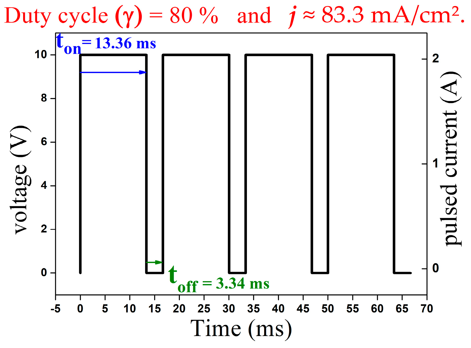
2.4. Parameterization Data from the Experiments

In Stage 1, the electrodeposition process utilized a pulsed current source delivering 10 V and 2 A to the system, with γ = 80% for 15 min within a temperature range of 28 °C to 30 °C. Additionally, Stage 1 included three experiments with electrode-to-sample distances varying between 2.75, 2.25, and 1.75 cm, and the concentration of MWCNTs used was 0.06 mg/mL. In Stage 2, the voltage, current, and duty cycles were kept constant, but the deposition time was extended to 60 min using an electrode-to-sample distance of 1.5 cm. Finally, in Stage 3, with the optimal parameters selected, the concentration of MWCNTs in the electrolytic solution was increased to 1 mg/mL, and the pulsed current source injected 10 V and 2 A into the system with a γ = 80% over a period of 120 min, with an electrode-to-sample distance of 1.5 cm. Figure 2 shows a flowchart of the experiments and procedures conducted, along with the parameters employed.

2.5. Morphological Characterization Using FEG-SEM

The micrographs were analyzed using a FEG-SEM obtained at the Institutional Laboratory of Scanning Electron Microscopy at the Museu Paraense Emílio Goeldi, using a TESCAN MIRA3® scanning electron microscope (TESCAN, Warrendale, PA, USA), equipped with a field emission gun (FEG). The samples were mounted on 12 mm diameter aluminum stubs using double-sided carbon adhesive tape. Subsequently, in order to make them conductive, they were gold (Au) sputter-coated for 2 h and 30 min, depositing an average thickness of 15 nm on the sample. The images were generated by secondary electron (SE) detection, using accelerating voltages between 5 and 15 kV and working distances ranging from 5 to 15 mm. An elementary mapping was obtained using an Energy Dispersive X-ray Spectroscopy—Scanning Electron Microscopy (EDS-SEM). This analysis was conducted using a TESCAN VEGA3® scanning electron microscope (TESCAN, Warrendale, PA, USA) at the voltage of 20 kV, a magnification of 2250×, and a working distance of 15 mm.

2.6. Vibrational Characterization Utilizing the Raman Spectroscopy Technique

To perform the vibrational analyses, the Raman spectroscopy technique was employed using the LabRAM HR Evolution® Confocal Raman Microscope from HORIBA France SAS (Longjumeau, France), located in the Vibrational Spectroscopy and High-Pressure Laboratory (LEVAP) of the Physics Graduate Program (PPGF) at the Federal University of Pará (UFPA), Belém campus. The laser line with a wavelength of 633 nm was used, along with a 100× objective lens, two accumulations with a time of 40 s, and ranges from 1200 to 2800 cm−1.

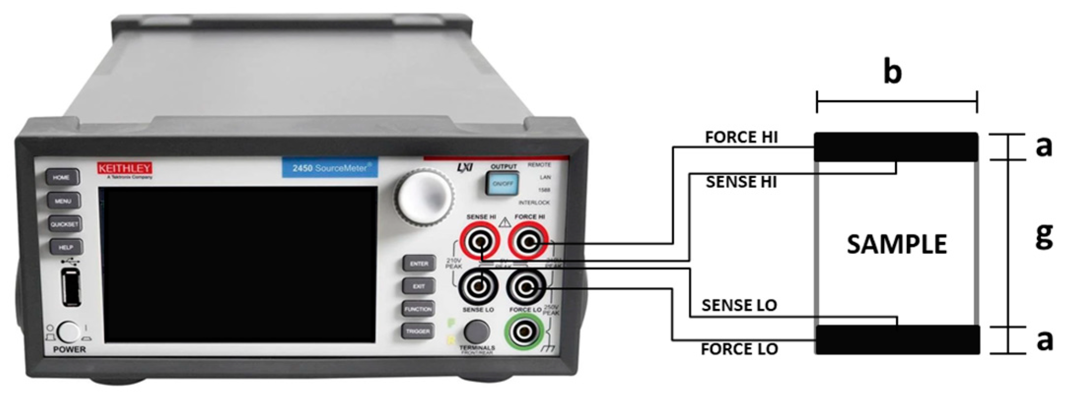
2.7. Surface Electrical Characterization Using the Four-Tip Kelvin Probe Technique

ASTM B3-13 [14] and ASTM B193-20 [15] are international standards used to measure the electrical conductivity of materials relative to pure annealed copper, the IACS. It is commonly used for volumetric conductivity. However, since this work analyzes the resistivity and electrical conductivity of aluminum foils without considering the cross-section, the measurements are performed in terms of surface resistivity and electrical conductivity rather than volumetric resistivity. On flat surfaces, it is necessary to measure surface resistance (Rs), for which the IACS for Testing and Materials (ASTM) D257-07 [16] can be used as a reference to obtain the surface resistivity ( ρ s ) and surface electrical conductivity ( σ s ) by applying the four-point Kelvin probe technique. Surface resistance data were measured for each sample replica using a KEITHLEY 2450® sourcemeter picoammeter (Keithley Instruments, Cleveland, OH, USA) with the assistance of the ASTM D257-07 (see Appendix A, Figure A1). In this way, ρ s (Ω) is defined by
ρ s = 2 a + b + 2 g R s g
where a is the width of the sensing electrode, b is its length, and g is the distance between the electrodes. Also, we can define σ s (S) as the inverse of electrical resistivity:
σ s = 1 ρ s

3. Results

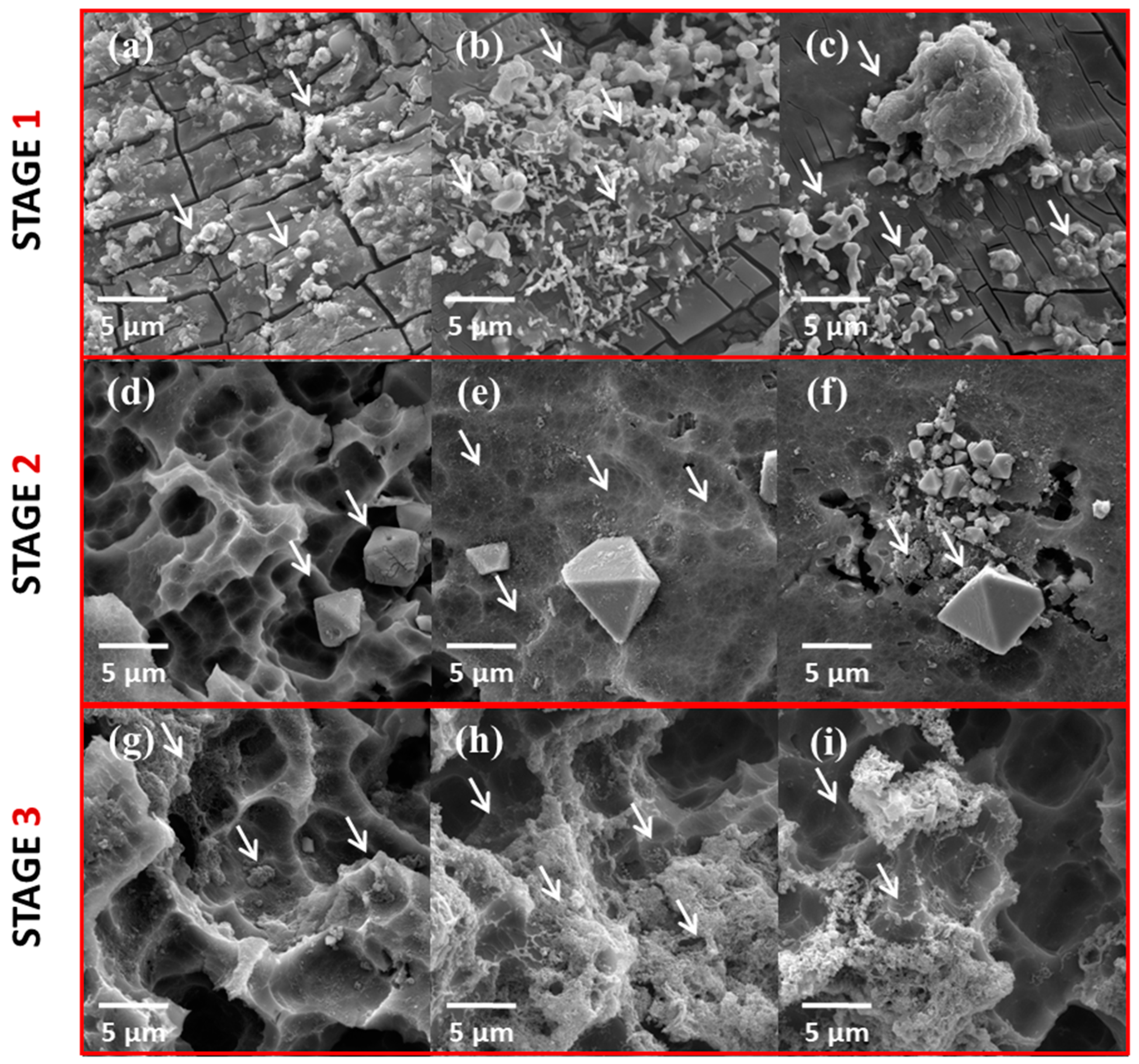
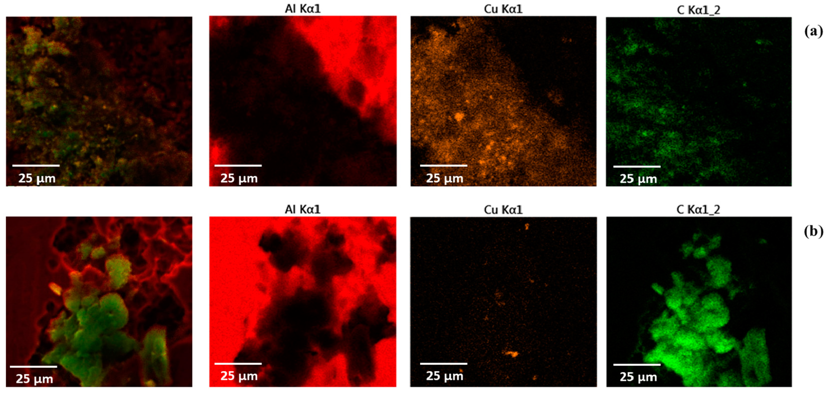
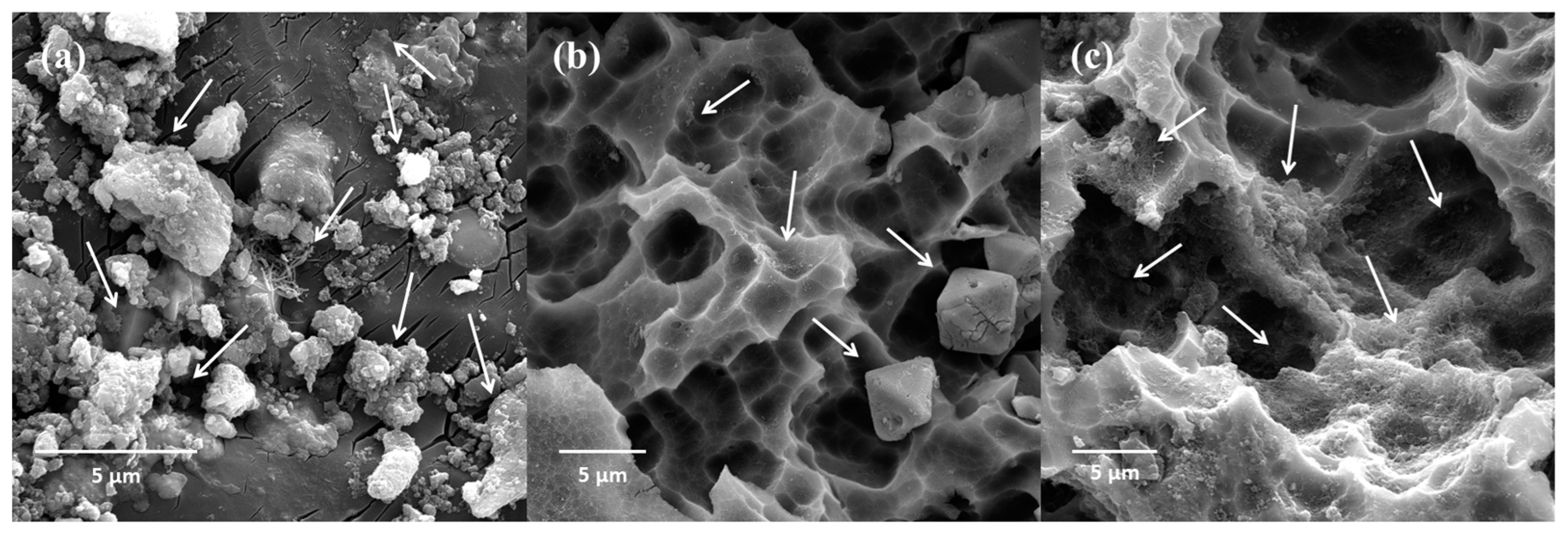
3.1. Morphological Analysis

The FEG-SEM micrographs of the samples corresponding to Stage 1 revealed a non-uniform dispersion of the Cu-MWCNT nanocomposite on the surface, characterized by the insertion of the nanocomposite within the Al2O3 layer in small concentrations. It was also possible to observe the presence of MWCNTs surrounded by the deposited copper (Figure 3a,b). In addition, the presence of clusters was observed in the deposited areas (Figure 3c). The presence of clusters can be attributed to agglomeration phenomena during the electrodeposition process, influenced by factors such as the concentration of MWCNTs in the solution and the electrochemical conditions. With the increase in the anodization time in Stage 2, high porosity was evidenced, where the aluminum matrix was significantly affected by the electric field in the anodic layer (Figure 3d). Furthermore, upward-facing concavities (pore embryos) of different sizes were observed (Figure 3e), and the presence of copper crystals was also observed (Figure 3d–f). Furthermore, the adhesion of agglomerated Cu-MWCNT nanocomposites close to the copper crystals could be observed (Figure 3f). Additionally, a detailed exploration of the samples in Stage 2 revealed that areas with larger pore diameters, averaging 12.6 μm, and larger concavities exhibited a greater tendency for MWCNTs to adhere to the surface. On the other hand, micrographs obtained at Stage 3 consistently revealed a uniform coating on the surface of the anodized substrate, demonstrating a homogeneous distribution of the Cu-MWCNT composite coating film; also notable is the robust concentration of MWCNTs in the pores (Figure 3g–i), an expected result with increasing the concentration of MWCNTs in the electrolyte solution for the electrodeposition process.
The EDS elemental mapping (Figure 4) shows the layered EDS image and the distribution of Al, Cu, and MWCNTs. Figure 4a shows the elemental distribution of the Cu-MWCNT composite coating the aluminum substrate in Stage 1, while Figure 4b shows the elemental distribution in Stage 3. Here, the presence of Al, Cu, and MWCNTs is represented by red, orange, and green regions, respectively. This analysis was conducted to investigate the distribution of Cu and MWCNTs on the surface of the anodized Al metallic substrate. Based on the EDS mapping results of the anodized samples coated with Cu-MWCNTs in Stages 1 and 3, a significant variation in the elemental composition of the coating was observed. In Stage 1, EDS elemental mapping revealed a predominant presence of Cu on the surface of the anodized aluminum. Due to the low concentration of nanotubes in the electrodeposition solution, the coating was primarily composed of Cu, showing less uniform and more superficial coverage of MWCNTs. In contrast, in Stage 3, the elemental composition changed significantly with an increased concentration of MWCNTs in the electrodeposition solution. The mapping showed that carbon was the dominant element on the surface, attributed to the presence of MWCNT agglomerations on the anodized surface. Therefore, it is evident that the coating in Stage 3 was dominated by MWCNTs, resulting in a denser coverage on the anodized aluminum substrate. Comparing the two stages, it is clear that the anodization process followed by pulsed electrodeposition alters not only the composition but also the morphology of the coating. The transition from a Cu-rich surface to one dominated by MWCNTs suggests structural changes that could potentially enhance the material’s electrical properties, as discussed later. Similar results have been reported in [12], associating increased electrical conductivity with the effectiveness of the nanostructured Cu and MWCNT coatings.

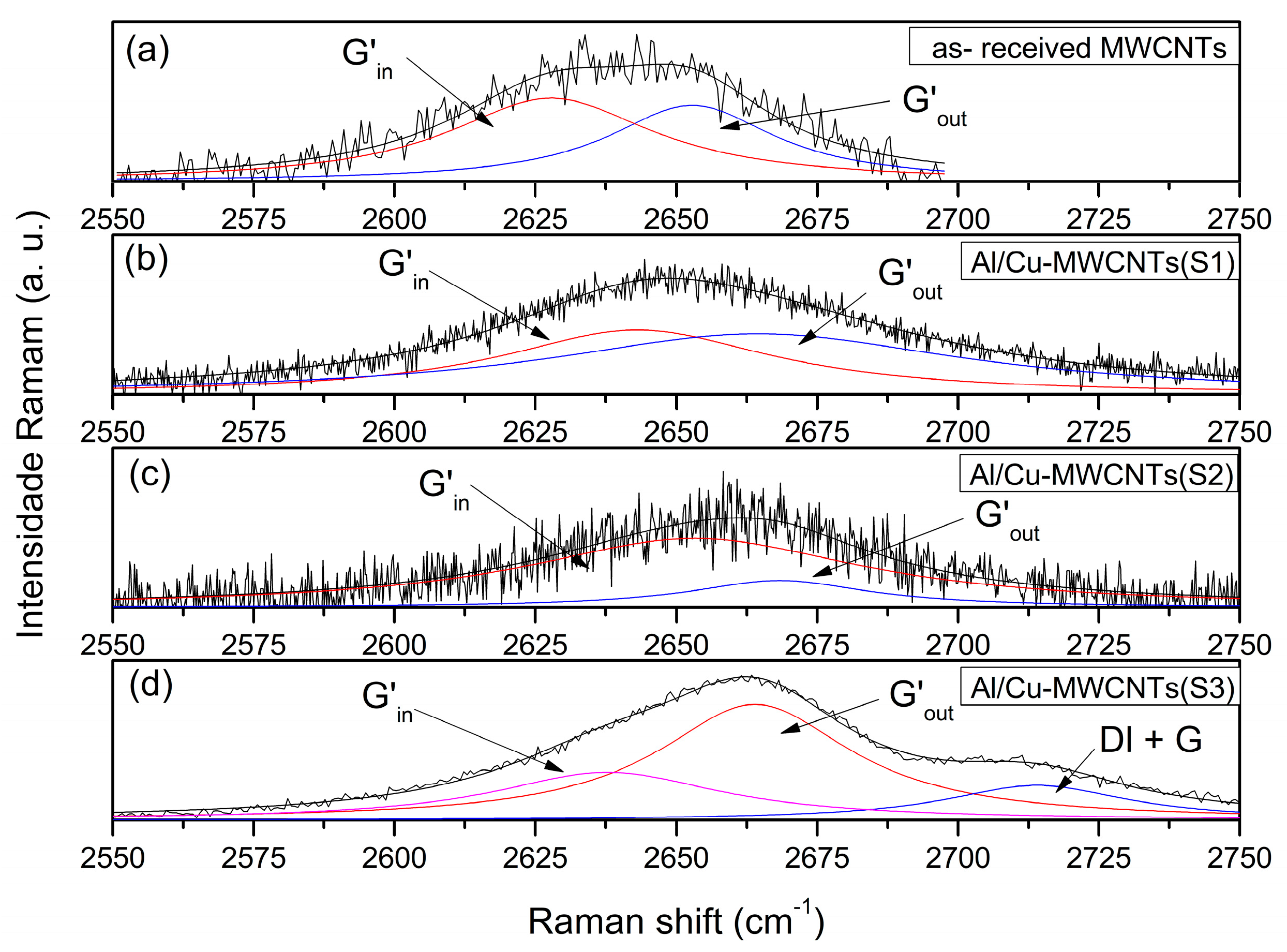
3.2. Analysis of Raman Spectra

It is possible to observe the deconvolutions obtained from Lorentzian functions, which present characteristic peaks of the sub-bands belonging to the D and G bands of the Raman scattering spectrum (see Appendix A, Figure A2). The D band is composed of satellite sub-bands shown through the peaks of the Lorentzians D1, Dr, DLO, and Dmiddle. They are associated with structural changes in the MWCNTs resulting from functionalization and the ultrasonication process, generating structural defects. On the other hand, the G band has two sub-bands: Gout and Gin, which are associated with the distribution of outer and inner diameters, respectively. Furthermore, in the G band, a peak called GBWF-like appears; the term “like” is due to the use of the Lorentzian function. This is due to the coupling of discrete phonons to the continuous electronic state; in short, it is a plasmon–phonon coupling mode [17,18]. This peak can also be observed in double- and triple-walled nanotubes, as well as in metallic nanotube bundles, for example, under pressure [19], temperature [20], and in the intercalation of particles between graphite layers [21], respectively. From a more specific perspective, the D’ sub-band identifies a double resonance of the D band, a phenomenon that reflects the microstructural complexity and intricate interaction between the components of the Cu-MWCNT composite and the aluminum matrix. The G’ spectrum profile of the samples exhibited two sub-bands (see Appendix A, Figure A3), as suggested by references [18]. The G’in sub-band is related to the distribution of diameters of innermost tubes, while the G’out corresponds to the distribution of diameters of outermost tubes. In summary, Table 2 presents the peak values centered on the D and G bands (first-order Raman scattering) and the G’ band (second-order scattering) obtained through deconvolutions with Lorentzian functions in the Raman spectrum.

3.3. Characterization of Electrical Properties

With the purpose of collecting average surface resistance R s values and calculating the surface electrical resistivity ρ s using the Kelvin probe technique, the following values were obtained in the replicas of each sample (see Appendix A, Table A1). Consequently, the average surface electrical conductivity values were achieved and compared with the control sample according to the data described in Table 3.

4. Discussion

4.1. Influence of Cu-MWCNT Morphology on Surface Electrical Conductivity Enhancement

The changes in parameters in the anodization and electrodeposition processes for the Cu-MWCNT coating played an indispensable role in enhancing the surface electrical conductivity of the 3003 aluminum alloy substrates. The high-resolution FEG-SEM images provided a detailed visualization of the anodic layer’s topography, revealing the intricate network of pores formed during the anodization process (Figure 5b,c). As observed, the anodization process, which created a porous alumina layer, and the pulsed electrodeposition technique ensured a homogeneous dispersion of Cu-MWCNTs on the aluminum surface, consistently indicating a uniform coating on the anodized substrate surface, as can be seen in Figure 5b,c, confirming the effectiveness of the pulsed electrodeposition technique after treating the aluminum surface with the formation of the anodic oxide layer. In fact, in Stage 1 (Figure 5a), it was observed that the pores were not effectively created, and that only after increasing the anodization time in the subsequent stages did they occur for a duration of 120 min. In addition, in Figure 5b, it is possible to observe the presence of copper crystals. Similar results can be found in the work of Rodrigues et al. [11]. In Stage 3 (Figure 5c), a higher concentration of the Cu-MWCNT composite coating the surface and interior of the pores created by the anodization process was observed due to the increase in the MWCNT concentration to a range between 0.9 and 1 mg/mL.
With the Cu-MWCNT nanocomposites well distributed over the anodized aluminum substrate, efficient pathways for electron transport were created, thus reducing resistance and increasing surface electrical conductivity. This improved morphology, characterized by uniform coverage and strong interfacial bonding, resulted in a notable increase in surface electrical conductivity from 337.62 S to 514.30 S (Figure 6) when comparing the Stage 3 sample to the control sample values.
Therefore, the integration of morphological analysis data and electrical properties supports the conclusion that the improvement in the composite coating led to a substantial enhancement in its electrical properties, resulting in a significant increase in the material’s surface electrical conductivity. This observation is particularly relevant, indicating a concomitant increase in surface electrical conductivity by ≈52.33%. On the other hand, in Figure A4a,b in Appendix A, a micrograph of the nanocomposite coating in another more porous region is shown. In Figure A4c,d in Appendix A, a smoother-looking coating together with the Al2O3 layer is displayed when compared to Figure A4a,b in Appendix A.

4.2. Correlation between Vibrational Property Changes and Coating Enhancement: A Blueshift Study in Raman Spectrum

The interaction between the MWCNTs and the matrix can lead to changes in the vibrational properties of the MWCNTs. In this study, with the increase/adjustments in the parameters and concentrations of nanotubes throughout the electrodeposition stages, shifts to higher frequencies (blueshift) of the G-band component for the outermost tubes were observed (Figure 7). This change suggests an electron transfer/loss during the deposition process to the working electrode, corroborating the improvement of the coating observed in the SEM images. Note that both the Full Width at Half Maximum (FWHM) and the intensity (not normalized) of the G band change even at low doping levels. That is, it is expected that as we use the carbon material, the FWHM (see Figure A5 in Appendix A for the Gout and Gin sub-bands for samples S2 and S3, respectively) and the intensity should decrease [22].
Indeed, a smaller FWHM indicates that vibrations are more concentrated around a specific frequency, while a larger width suggests a broader distribution of vibrational frequencies. Therefore, even if we cannot use the frequencies of the Gin and Gout to monitor the doping level, the observed changes in FWHM and positions (Figure 7) suggest some doping mechanism in the distribution of the outermost nanotubes. Thus, the increases in the FWHM of the Gout and Gin sub-bands observed in Table A1 and Table A2 of Appendix A suggest an intensification of doping effects in the Al/Cu-MWCNTs(S3) samples compared to the as-received MWCNTs and the composites generated in previous stages. This information points to a high density of defects created in this composite [11,23].
It is known that when compared to the G band, the G’ band is more sensitive to the doping effect [24,25]. When comparing each electrodeposited sample of Al/Cu-MWCNTs to the as-received MWCNTs sample, a significant variation in the position of the G’ band and the FWHM is observed, which is a strong evidence of charge transfer during the electrodeposition process. This doping process reveals a decrease/increase in the FWHM of both G’in and G’out components, by −3 cm−1 and 4 cm−1 as can be seen in Figure 8, respectively, which has been observed in [18,24]. Similarly to the G band, both G’ components show shifts to higher frequencies, as shown in Table 1. Focusing solely on the outermost tube component, to corroborate the observations made in the G band, it was found that the blueshift for the Al/Cu-MWCNTs(S3) sample was ≈ 16 cm−1 compared to the as-received MWCNT sample. This shift is due to experimental adjustments made in this stage and the pulsed current process injecting high current density in each pulse, allowing for both process speed and improved coating with the composite.

4.3. Analysis of Defect Density and Amorphous Carbon Content

Alternatively, a detailed investigation was conducted at various stages of the electrodeposition process, revealing an increase in the defect density in the outermost nanotubes. This assessment was made based on the IDr/IGout ratio (Figure 9). As observed in Table 2, there was an increase in the amount of amorphous carbon in the Al/Cu-MWCNTs(S3) composite, as revealed by the Dmiddle sub-band. Furthermore, the ratio between the areas of the Dmiddle sub-band and the G band, known as the Amorphous Carbon Degree (ACD), indicates the amount of amorphous carbon in the sample [11,26] which refers to the sp3 and sp2 bond sites according to equation
ACD = [ ∑ rel. area (Dmiddle)/∑ rel. area (Gin + Gout)] × 100%
In comparison to the as-received MWCNT sample, which has an ACD value of ≈12.97% (Figure 9), this finding is of significant importance as it demonstrates an increase/decrease in defect density following each stage of the preparation and electrodeposition processes of the nanocomposites, aligning with theoretical expectations. In fact, when we analyzed the defect concentrations of Samples S2 and S3, we observed that there was a decrease in defects. Even with this decrease, there is an indication of amorphous carbon that did not affect the surface electrical conductivity findings, and is therefore an indication of an increase in the crystallinity of the nanotubes. This same result was verified in work [11].
Additionally, it should be considered that during the anodization stage of aluminum, the incorporation of anions occurs due to the injection of electrons into the oxide conduction band in an avalanche process [27,28]. This causes the anions to be distributed within the oxide layer closer to the metal/oxide interface [29]. On the other hand, aluminum oxide is an n-type semiconductor, and under a cathodic polarization at the working electrode, p-type doping was induced on the Cu-MWCNT composite. Furthermore, with an increase of approximately 16.7 times in the concentration of milligrams of MWCNTs per milliliter of solution and an increase to 1 h of pulsed current time, there is an increase in current density, thus promoting a rapid reaction on the electrode surface, leading to more ions from the composite being conducted from the electrolytic solution, resulting in better dispersion and consequently achieving a larger coated area on the metal surface. This is supported by the electrical results of surface conductivity, along with the overlapping of the nanocomposite on the “pore embryos”, compacting each other onto the metal surface.

5. Conclusions

Nanotechnology has revolutionized various fields of material research and development, with particular emphasis on improving the structural and functional properties of conventional materials. In this context, aluminum, a metal widely used due to its lightness and good conductivity, can have its properties significantly enhanced by the addition of copper and MWCNTs. The process of anodization followed by pulsed electrodeposition was chosen for its ability to create a porous Al2O3 layer that facilitates the uniform incorporation of nanocomposites. Thus, the incorporation of copper and MWCNTs into aluminum substrate using the anodization process followed by pulsed electrodeposition was investigated with the aim of enhancing the surface electrical conductivity and morphological properties of the anodized aluminum surface, creating a Cu-MWCNT nanocomposite coating.
Morphological analysis by FEG-SEM revealed that, in the first stage, there was a non-uniform dispersion of the Cu-MWCNT nanocomposites on the aluminum surface, characterized by significant agglomerations. This was attributed to agglomeration phenomena during the electrodeposition process, influenced by the concentration of MWCNTs in the solution and electrochemical conditions. The insertion of nanocomposites into the Al2O3 layer and the presence of MWCNTs surrounded by deposited copper were observed. With the increased anodization time in the second stage, an improvement in porosity was evidenced with the creation of pores averaging diameters of 12.6 μm, increasing the surface area of the substrate in the anodic layer for the Cu-MWCNT nanocomposite coating. The third stage demonstrated a uniform coating on the surface of the anodized substrate, with a homogeneous distribution of Cu-MWCNTs.
Raman spectroscopy analysis provided details on the structural changes in MWCNTs reflected in the D, G, and G’ bands. Shifts to higher frequencies were observed, confirming charge transfer and structural changes occurring in the material, corroborating the morphological results of the coating. The intensification of doping effects was confirmed with the changes observed in the FWHM of the sub-bands belonging to the G and G’ bands. A significant increase in defect density, based on the IDr/IGout ratio, and in the amorphous carbon content with an increase in the ACD value of ≈12.97% was observed compared to the as-received MWCNT samples.
The electrical analysis results showed a remarkable increase in surface electrical conductivity, with an increment of ≈52.33%. This increase is attributed to the creation of efficient pathways for electron transport due to the homogeneous distribution of Cu-MWCNT nanocomposites and strong interfacial bonding, resulting in improved morphology and electrical properties with the Cu-MWCNT coating.
Therefore, the anodization process followed by pulsed electrodeposition was demonstrated to be an effective technique for incorporating Cu-MWCNT nanocomposites into anodized aluminum surfaces. This method not only improved the surface electrical conductivity but also provided a homogeneous coating, enabling its use in applications where enhanced electrical and structural properties are essential.

Author Contributions

Conceptualization, A.S.S., E.M.B., M.E.S.S. and M.A.L.R.; methodology, A.S.S., M.E.S.S. and M.A.L.R.; formal analysis, A.S.S., M.E.S.S. and M.A.L.R.; investigation, A.S.S. and M.E.S.S.; resources, E.M.B. and M.A.L.R.; data curation, A.S.S. and M.E.S.S.; writing—original draft preparation, A.S.S.; writing—review and editing, M.E.S.S.; supervision, M.E.S.S. and M.A.L.R. All authors have read and agreed to the published version of the manuscript.

Funding

This research was supported by the CNPq (381396/2023-1).

Data Availability Statement

The original contributions presented in the study are included in the article, further inquiries can be directed to the corresponding author.

Acknowledgments

The authors gratefully acknowledge PROPESP/UFPA (PAPQ) for payment of publication fees; A.S.S. and M.E.S.S. thank CNPq for individual financial support; The Graduate Program in Materials Science and Engineering (PPGCEM/UFPA), Ananindeua campus; the Institutional Laboratory of Scanning Electron Microscopy at the Research campus -Museu Paraense Emílio Goeldi, Pará, Belém; the Vibrational Spectroscopy and High Pressure Laboratory (LEVAP) of the Physics Graduate Program (PPGF) at the Federal University of Pará (UFPA), Guamá campus; Thanks to the LCAM/UFPA for technical support during the analyses; the 3D Nanostructuring Laboratory at the Federal University of Pará—Belém Campus; and the National Council for Scientific, Technological Development (CNPq) and Soli Deo Gloria, Amen.

Conflicts of Interest

The authors declare no conflicts of interest. The funders had no role in the design of the study; in the collection, analyses, or interpretation of data; in the writing of the manuscript; or in the decision to publish the results.

Appendix A

Figure A1. Wiring diagram of the KEITHLEY 2450 sourcemeter picoammeter used in electrical characterization with the assistance of ASTM D257-07 standard and the four-point Kelvin probe technique, where a, b are the dimensions of the test electrode and g is the distance between the electrodes in the measurement.
Metals 14 01060 g0a1
Figure A2. Raman spectrum of the D and G bands and their sub-bands related to the as-received MWCNTs and to the Al/Cu-MWCNT(S1), Al/Cu- MWCNT(S2), and Al/Cu MWCNT(S3) composites. It is possible to observe the deconvolutions obtained from Lorentzian functions, which present characteristic peaks of the sub-bands belonging to the D bands and G bands of the Raman scattering spectrum.
Metals 14 01060 g0a2
Figure A3. Raman spectrum of the G’ bands and their sub-bands related to the as-received MWCNTs and to the Al/Cu-MWCNT(S1), Al/Cu-MWCNT(S2), and Al/Cu-MWCNT(S3) composites. Raman spectrum of the G’ bands and their subbands related to the received MWCNTs and the compounds Al/Cu-MWCNTs(S1), Al/Cu-MWCNTs(S2) and Al/Cu-MWCNTs(S3) shown in Figure A3a, Figure A3b, Figure A3c and Figure A3d respectively. It is possible to observe the deconvolutions obtained from Lorentzian functions, which present characteristic peaks of the sub-bands belonging to the G’ bands of the Raman scattering spectrum.
Metals 14 01060 g0a3
Table A1. ρ s (Ω) values of the control, Al/Cu-MWCNT(S1), Al/Cu- MWCNT(S2), and Al/Cu-MWCNT(S3) samples.
SampleControlAl/Cu- MWCNTs (S1)Al/Cu- MWCNTs (S2)Al/Cu- MWCNTs (S3)
ρ s (Ω)0.00296 ± 9.02 × 10−50.00261 ± 1.48 × 10−40.00231 ± 4.90 × 10−50.00195 ± 3.69 × 10⁻⁵
all values were obtained using ASTM D257-07.
Figure A4. Micrographs in another region of interest of aluminum coated with Cu-MWCNT nanocomposite at Stage 3: (a) 9.23 k × magnification highlighting the porosity of the region and high concentration of Cu-MWCNTs deposited, (b) 55.4 k × magnification showing in greater detail the high concentration of Cu-MWCNTs, (c) 9.23 k × magnification revealing the uniformity of the Cu-MWCNT coating, and (d) 55.4 k × magnification showcasing the appearance of a region formed by aluminum oxide and the uniform coating of the Cu-MWCNT film.
Metals 14 01060 g0a4
Figure A5. Broadening and narrowing of the FWHM to the outer and inner G sub-bands comparing the Al/Cu-MWCNT(S1), Al/Cu-MWCNT(S2), and Al/Cu-MWCNT(S3) samples with as-received MWCNTs.
Metals 14 01060 g0a5
Table A2. FWHM * values of the as-received MWCNTs, Al/Cu-MWCNT(S1), Al/Cu-MWCNT(S2) and Al/Cu-MWCNT(S3) samples for G and G’ sub-bands.
SampleGoutGinG’inG’out
as-received MWCNTs27 ± 3.025 ± 3.045 ± 2.536 ± 3
Al/Cu-MWCNTs(S1)33 ± 3.033 ± 3.081 ± 3.057 ± 2.5
Al/Cu-MWCNTs(S2)25 ± 3.228 ± 4.072 ± 3.038 ± 3.0
Al/Cu-MWCNTs(S3)29 ± 4.018 ± 4.040 ± 2.234 ± 2.1
* all values are in cm−1.

References

  1. Chen, S.; Fu, S.; Liang, D.; Chen, X.; Mi, X.; Liu, P.; Zhang, Y.; Hui, D. Preparation and properties of 3D interconnected CNTs/Cu composites. Nanotechnol. Rev. 2020, 9, 146–154. [Google Scholar] [CrossRef]
  2. Geng, H.; Chen, B.; Wan, J.; Shen, J.; Kondoh, K.; Li, J.S. Matrix effect on strengthening behavior of carbon nanotubes in aluminum matrix composites. Mater. Charact. 2023, 195, 112484. [Google Scholar] [CrossRef]
  3. Zhang, S.L.; Nguyen, N.; Leonhardt, B.; Jolowsky, C.; Hao, A.; Park, J.G.; Liang, R. Carbon-Nanotube-Based Electrical Conductors: Fabrication, Optimization, and Applications. Adv. Mater. Technol. 2019, 5, 1800811. [Google Scholar] [CrossRef]
  4. Gonçalves, I.L.; Vinhosa, R.A.; de Freitas, D.S.; Brasil, S.L. Pulsed electrophoretic deposition of hybrid coatings from aqueous suspensions as surface functionalization and sealing technique of anodized AA2024. Part I: Morphological characterization, analysis of the interfacial interactions, and evaluation of pore impregnation of the anodic layer. Prog. Org. Coat. 2023, 178, 107474. [Google Scholar]
  5. Zhang, J.; Cheng, F.; Wang, L.; Xu, Y.; Zhou, Z.; Liu, X.; Hu, Y.; Hu, X. Reinforcement study of anodizing treatment with various temperatures on aluminum substrates for stronger adhesive bonding with carbon fiber composites. Surf. Coat. Technol. 2023, 462, 129473. [Google Scholar] [CrossRef]
  6. Zulkifli, F.W.A.; Yazid, H.; Jani, A.M.M. Immobilization of carbon nanotubes decorated gold nanoparticles on anodized aluminium oxide (Au-CNTs-AAO) membrane for enhanced catalytic performance. Mater. Chem. Phys. 2021, 264, 12444. [Google Scholar] [CrossRef]
  7. Daryadel, S.; Behroozfar, A.; Morsali, S.R.; Moreno, S.; Baniasadi, M.; Bykova, J.; Bernal, R.A.; Minary-Jolandan, M. Localized pulsed electrodeposition process for three-dimensional printing of nanotwinned metallic nanostructures. Nano Lett. 2018, 18, 208–214. [Google Scholar] [CrossRef]
  8. Magalhães, R.; Proenca, M.P.; Araújo, J.P.; Nunes, C.; Pereira, A.M.; Sousa, C.T. Fabrication of FePt nanowires through pulsed electrodeposition into nanoporous alumina templates. Appl. Nanosci. 2022, 12, 3573–3584. [Google Scholar] [CrossRef]
  9. Fan, H.; Zhao, Y.; Wang, S.; Ma, R. Improvement of microstructures and properties of copper-aluminium oxide coating by pulse jet electrodeposition. Mater. Res. Express 2019, 6, 115090. [Google Scholar] [CrossRef]
  10. Xu, M.; Yue, G.; Bizzotto, D.; Asselin, E. Electrodeposition of aluminum onto copper-coated printed circuit boards. J. Electrochemic. Soc. 2017, 164, D729. [Google Scholar] [CrossRef]
  11. Rodrigues, F.; Pinheiro, P.; Sousa, M.; Angélica, R.; Paz, S.; Reis, M. Electrical Properties of Iodine-Doped Cu/f-CNT Coated Aluminum Wires by Electrophoresis with Copper Sulfate Solution. Metals 2022, 12, 787. [Google Scholar] [CrossRef]
  12. Mandal, P.; Mondal, S.C. Investigation of Electro-Thermal property for Cu-MWCNT composite coating on anodized 6061 aluminium alloy. Appl. Surf. Sci. 2018, 454, 138–147. [Google Scholar] [CrossRef]
  13. Bazbouz, M.B.; Aziz, A.; Copic, D.; De Volder, M.; Welland, M.E. Fabrication of high specific electrical conductivity and high ampacity carbon Nanotube/Copper composite wires. Adv. Electron. Mater. 2021, 7, 2001213. [Google Scholar] [CrossRef]
  14. ASTM B3-13; Standard Specification for Soft or Annealed Copper Wire. American Society for Testing and Materials: West Conshohocken, PA, USA, 2018.
  15. ASTM B193 20; Standard Test Method for Resistivity of Electrical Conductor Materials. American Society for Testing and Materials: West Conshohocken, PA, USA, 2020.
  16. ASTM D257-07; Standard Test Methods for DC Resistance or Conductance of Insulating Materials. American Society for Testing and Materials: West Conshohocken, PA, USA, 2012.
  17. Brown, S.D.M.; Jorio, A.; Corio, A.P.; Dresselhaus, M.S.; Dresselhaus, G.; Saito, R.; Kneipp, K. Origin of the Breit-Wigner-Fano lineshape of the tangential G-band feature of metallic carbon nanotubes. Phys. Rev. B 2001, 63, 155414. [Google Scholar] [CrossRef]
  18. Oliveira, A.C.; Reis, M.A.L.; De Sousa, F.F.; Sousa, M.E.S. Doping charge transfer in Pt/CNT systems induced by laser power heating. Chem. Phys. 2020, 530, 110591. [Google Scholar] [CrossRef]
  19. Alencar, R.S.; Aguiar, A.L.; Paschoal, A.R.; Freire, P.T.C.; Kim, Y.A.; Muramatsu, H.; Endo, M.; Terrones, H.; Terrones, M.; San-Miguel, A.; et al. Pressure-induced selectivity for probing inner tubes in double-and triple-walled carbon nanotubes: A resonance raman study. J. Phys. Chem. C 2014, 118, 8153–8158. [Google Scholar] [CrossRef]
  20. Uchida, T.; Tachibana, M.; Kurita, S.; Kojima, K. Temperature dependence of the Breit–Wigner–Fano Raman line in single-wall carbon nanotube bundles. Chem. Phys. Lett. 2004, 400, 341–346. [Google Scholar] [CrossRef]
  21. Eklund, P.C.; Dresselhaus, G.; Dresselhaus, M.S.; Fischer, J.E. Raman scattering from in-plane lattice modes in low-stage graphite-alkali-metal compounds. Phys. Rev. B 1977, 16, 3330. [Google Scholar] [CrossRef]
  22. Lazzeri, M.; Mauri, F. Nonadiabatic Kohn Anomaly in a Doped Graphene Monolayer. Phys. Rev. Lett. 2006, 97, 266407. [Google Scholar] [CrossRef]
  23. Brito, P.R.; Loayza, C.R.; Sousa, M.E.; Braga, E.M.; Angélica, R.S.; da Paz, S.P.; Reis, M.A. Cast aluminum surface reinforced with carbon nanotube via solubilization treatment. Met. Mater. Int. 2022, 28, 802–810. [Google Scholar] [CrossRef]
  24. Yan, J.; Henriksen, E.A.; Kim, P.; Pinczuk, A. Observation of anomalous phonon softening in bilayer graphene. Phys. Rev. Lett. 2008, 101, 136804. [Google Scholar] [CrossRef] [PubMed]
  25. Das, A.; Chakraborty, B.; Piscanec, S.; Pisana, S.; Sood, A.K.; Ferrari, A.C. Phonon renormalization in doped bilayer graphene. Phys. Rev. B 2009, 79, 155417. [Google Scholar] [CrossRef]
  26. Dos Reis, M.A.L.; Barbosa Neto, N.M.; De Sousa, M.E.S.; Araujo, P.T.; Simões, S.; Vieira, M.F.; Viana, F.; Loayza, C.R.L.; Borges, D.J.A.; Cardoso, D.C.S.; et al. Raman spectroscopy fingerprint of stainless steel-MWCNTs nanocomposite processed by ball-milling. AIP Adv. 2018, 8, 015323. [Google Scholar] [CrossRef]
  27. Ikonopisov, S. Theory of electrical breakdown during formation of barrier anodic films. Electrochim. Acta 1977, 22, 1077–1082. [Google Scholar] [CrossRef]
  28. Montero, I.; Albella, J.M.; Martinez-Duart, J.M. Influence of Electrolyte Concentration on the Anodization and Breakdown Characteristics of Ta2O5 Films. J. Electrochem. Soc. 1985, 132, 814. [Google Scholar] [CrossRef]
  29. Parkhutik, V.P. The initial stages of aluminium porous anodization studied by Auger electron spectroscopy. Corros. Sci. 1986, 26, 295–310. [Google Scholar] [CrossRef]
Figure 1. Dynamics of the duty cycle ( γ ) used in the Cu-MWCNT electrodeposition process showing Ton and Toff, relating the applied voltage of 10 V and the peak current of 2 A injected into the system.
Metals 14 01060 g001
Figure 2. Flowchart depicting the sequence of experiments, stages, and parameters used.
Metals 14 01060 g002
Figure 3. Micrographs of aluminum samples coated with the Cu-MWCNT nanocomposite at different stages of the experiments: (ac) samples obtained in Stage 1 showing the adhesion of the composite to the aluminum oxide layer at 9.23 k × magnification; (df) morphology of the pores created during anodization and the presence of copper crystals in octahedral shape at 9.23 k × magnification; (gi) high porosity of the region due to the action of the electric field in the formation of the anodic layer, highlighting the high concentration of nanotubes adhered to the region at 9.23 k × magnification.
Metals 14 01060 g003
Figure 4. EDS distribution elemental mapping of Al, Cu, and MWCNTs in (a) Al/Cu-MWCNTs(S1) coating and (b) Al/Cu-MWCNTs(S3) coating.
Metals 14 01060 g004
Figure 5. Micrographs of aluminum samples coated with the Cu-MWCNT nanocomposite: Stage 1 with 17.3 k × magnification (a), Stage 2 with 9.23 k × magnification (b), and Stage 3 with 9.23 k × magnification (c), showing the progression of the coating within the porous aluminum oxide layer.
Metals 14 01060 g005
Figure 6. Surface electrical conductivity (S) comparing the control, Al/Cu-MWCNTs(S1), Al/Cu-MWCNTs(S2), and Al/Cu-MWCNTs(S3) samples.
Metals 14 01060 g006
Figure 7. Displacement of the Gout band to higher frequencies due to CNT addition.
Metals 14 01060 g007
Figure 8. Broadening and narrowing of the FWHM to the outer and inner G’ sub-bands comparing the Al/Cu-MWCNTs(S1), Al/Cu- MWCNTs(S2), and Al/Cu-MWCNTs(S3) samples with the as-received MWCNTs.
Metals 14 01060 g008
Figure 9. Peak intensity ratios related to defects and graphitization of the outermost tubes IDr/IGout most and ACD%.
Metals 14 01060 g009
Table 1. Chemical composition limit data for aluminum alloy 3003.
ComponentSiFeCuMnZiOthersAl
Chemical composition limits (%)0.60.70.05 a 0.21 a 1.50.10.15remainder
Table 2. Raman peaks obtained through Lorentzian deconvolutions (cm−1).
SampleDlDrDLODmiddleGBWF-likeGoutGinD’G’inG’out
as-received MWCNTs1315132813531486-15671583160226282653
Al/Cu-MWCNTs(S1)1315132913461484154215731588160826352668
Al/Cu-MWCNTs(S2)1320133713991512155715761596161726532668
Al/Cu-MWCNTs(S3)1330134713781491156315831598161726642714
The emergence of this vibration mode is due to the compression of the nanotubes in bundles during the transport of the nanocomposite, induced by the electric field forces during electrodeposition process, for this reason in the as-received MWCNTs sample this effect was not observed.
Table 3. Values of surface electrical conductivity as a function of the average ρ s in the control, Al/Cu-MWCNTs(S1), Al/Cu- MWCNTs(S2), and Al/Cu-MWCNTs(S3) samples.
SampleControlAl/Cu- MWCNTs (S1)Al/Cu- MWCNTs (S2)Al/Cu- MWCNTs (S3)
σ s (S)337.62 ± 10.1383.83 ± 22.3432.20 ± 9.2514.30 ± 9.7
values calculated using Equation (3).
Disclaimer/Publisher’s Note: The statements, opinions and data contained in all publications are solely those of the individual author(s) and contributor(s) and not of MDPI and/or the editor(s). MDPI and/or the editor(s) disclaim responsibility for any injury to people or property resulting from any ideas, methods, instructions or products referred to in the content.

