Article

Evaluation of Solidification and Interfacial Reaction of Sn-Bi and Sn-Bi-In Solder Alloys in Copper and Nickel Interfaces

by
Jaderson Rodrigo da Silva Leal
1,
Rodrigo André Valenzuela Reyes
1,
Guilherme Lisboa de Gouveia
1,
Francisco Gil Coury
2 and
José Eduardo Spinelli
2,*
1
Graduate Program in Materials Science and Engineering, Federal University of Sao Carlos, Sao Carlos 13565905, SP, Brazil
2
Department of Materials Engineering, Federal University of Sao Carlos–UFSCar, Sao Carlos 13565905, SP, Brazil
*
Author to whom correspondence should be addressed.
Metals 2024, 14(9), 963; https://doi.org/10.3390/met14090963 (registering DOI)
Submission received: 16 July 2024 / Revised: 22 August 2024 / Accepted: 23 August 2024 / Published: 25 August 2024

Abstract

:
Although there are studies devoted to lower Indium (In) addition, Sn-Bi alloys containing 10 wt.% In or more have been barely investigated so far. Higher In contents may offer the potential for improved joint production, better control over the growth of interfacial layers, and enhanced mechanical strength. The present article focuses on the solidification, wettability, adhesion strength, and interfacial intermetallic growth in the Sn-40%Bi-10%In alloy soldered on Cu and Ni pads. SEM-EDS, wettability tests, and tensile tests were performed. The contact angles were measured in Cu and Ni as 24° and 26°, respectively. Indium addition promoted coarsening of the as-solidified microstructure due to an increase in the alloy solidification range. The Bi spacing was increased at least three times, with a strong segregation of Bi towards the interface. The formation and growth of alloy/Cu reaction layers were also evaluated under the different aging conditions of the as-soldered joints, simulating real service. A growth kinetics model of the reaction layer showed that In increases the activation energy, thereby reducing the layer growth. The adhesions of the formed intermetallics films in Cu and Ni were analyzed using tensile tests. It was observed that the alloy/Ni couple exhibited better adhesion. Premature fracturing appears to happen in the alloy/Cu joint due to the higher intermetallic compound’s (IMC) thickness, rough morphology, and coarser microstructure. Both ductile fracture features with dimples and cleavage zones associated with Bi, Cu6(Sn,In)5, and Ni3Sn4 intermetallics were observed.

1. Introduction

Solder materials play an essential role in ensuring the mechanical and electrical integrity of components. Among the various solder alloys, In-containing Sn-Bi alloys have garnered significant attention due to some favorable features, such as low melting points and suitable wettability [1,2]. Sn-Bi-In alloys are suitable for low-temperature applications. Furthermore, the presence of In was demonstrated to enhance heat dissipation in electronic systems with high power density [3]. Trends in electronic packaging are shifting towards miniaturization, high-density packaging, and enhanced performance. The demands for rapid data communication in 5G and IoT (Internet of Things) applications are driving the development of various packaging technologies, including System-in-Package (SiP), Wafer-Level Packaging (WLP), System-on-Chip (SoC), and System Integration Package (SIP) [1]. To support these technologies and prevent issues related to thermal expansion and deformation while minimizing their defects, there is an increasing need for research on low-melting-point solders, such as Sn-Bi, Sn-In, or Sn-Bi-In alloys [2]. Sn-Bi solder is more cost-effective compared to Sn-In and offers better thermal reliability due to its relatively higher melting temperature.
Low-temperature solder (LTS) alloys have become a promising solution for the electronics industry. They not only advance technology, but also support the global move towards sustainability. Typically melting below 180 °C, these solders represent a significant reduction in temperature compared to traditional options. This lower temperature not only saves energy, but also minimizes the risk of damaging delicate components, making them suitable for eco-friendly manufacturing. The environmental benefits of LTS include reduced energy consumption, extended product lifespan, and less material waste [3].
This introduction focus on three fundamental aspects of these alloys: solidification, wettability, and the formation of the intermetallic Cu6Sn5 layer, which collectively influence the quality of solder joints.
Solidification involves the transition of the alloy from a liquid state to a solid state, a transformation that significantly impacts the microstructure [4] and, consequently, the properties of the solder joint. Indium (In) can significantly alter the solidification behavior of the alloy. Liquid undercooling plays a central role in determining the solidification’s microstructure. Indium can reduce both the liquidus temperature and undercooling, facilitating the maximum number of nuclei to initiate grain formation. Therefore, more refined microstructures could be expected. Furthermore, the growth stage during solidification can be influenced by the distribution of In within the alloy. In can segregate at the dendrite boundaries, which can modify the growth dynamics. A uniform microstructure in soldered joints may be advantageous, as it can enhance the mechanical stability and reliability, especially under thermal cycling conditions commonly encountered in electronic applications. Wu et al. [5] demonstrated the impacts of increasing In content in the Sn-40 wt.% Bi alloy based on the microstructure formed for different In contents. For low In contents (1, 2, and 4 wt.%), the microstructure consisted of In in solutions in β-Sn dendrites and Bi precipitates. For higher contents (6 and 8 wt.%), the microstructure comprised β-Sn, BiIn, and Bi phases. These changes in microstructure can lead to significant alterations in mechanical properties as well as a reduction in melting temperature. To the authors’ knowledge, very few studies have been found in the literature regarding the solidification of Sn-Bi-In alloys with higher In contents (>8 wt.%).
Bi is denser than Sn. As such, there is a pronounced tendency for Bi segregation during solidification, which is recognized as a drawback of Sn-Bi alloys [6]. The impact of In on the Bi segregation in solder joints is still a problem to be addressed. Moreover, the coarsening rate of the eutectic Bi phase may also be influenced by In. Coarser Bi tend to increase the joint’s brittleness, decreasing the adhesion strength. The substrate also plays a key role on the solidification and quality of soldered joints in electronics components. The main substrates used are gold (Au), platinum (Pt), palladium (Pd), nickel (Ni), Fe-42% Ni (INVAR), and especially copper (Cu) [7]. Understanding the simultaneous effects of In and the substrate is important, as they both affect the heat flux at the solder alloy/substrate interface and thus contribute to the solidification process and the microstructure of the soldered joints [8]. Overall, studies to understand the solidification kinetics in substrates for microelectronics tend to have a more fundamental nature, especially focusing on the relationships between microstructural spacings and solidification parameters.
Wettability is another factor in the performance of soldering materials. It refers to the ability of the molten solder to spread on the surface of a substrate, forming a continuous and adherent joint. Good wettability is essential for guaranteeing the solder’s quality. Sn-Bi-In alloys exhibit excellent wettability, which can be attributed to the presence of In [9]. In induces low surface tension [9], which enhances the spreading behavior of the molten solder on the pad. Among several important characteristics for soldering, the degree of wetting between the solder alloy and the substrate, which is measured using the contact angle (θ), is the most frequently studied and documented for several Sn-based alloys [10], whereas it is less explored for Sn-Bi-In alloys.
In soldering for electronic micro-components, it is important for the intermetallic compound (IMC) layer to be thin to ensure strong metallurgical bonds. Excessive IMC thickness can weaken the solder joint and cause degradation over time, which is a major concern in the electronics industry [1]. Understanding the kinetics of interfacial reactions, which are driven by atomic diffusion during solidification, is fundamental to control the processes and the solder quality. Additionally, substrate dissolution during soldering can alter the alloy’s composition and create unexpected phases, further complicating the process.
In the case of In-containing Sn-Bi alloys, the formation of the Cu6Sn5 layer is also significant. The Cu6Sn5 layer forms at the interface between the solder and the copper substrate. The Cu6Sn5 layer is formed through a diffusion process during soldering, where tin (Sn) from the solder reacts with copper (Cu) from the substrate. Indium can diffuse into the Cu6Sn5 layer, potentially altering its properties and stability. Li et al. [11] investigated the Sn-50Bi-12In, Sn-44Bi-12In, and Sn-38Bi-12In alloys in copper substrates and demonstrated that the IMC’s layer was mainly composed of Sn and Cu elements. It was inferred that the Cu6Sn5 was predominant at the interface. The results also showed that, for lower Bi content, the total thickness of the IMC layer decreased. The thickness and uniformity of the IMC layer are critical parameters that determine the mechanical strength and reliability of the solder joint. A thin and uniform Cu6Sn5 layer can provide a strong bond. Conversely, an excessively thick or irregular Cu6Sn5 layer can lead to brittleness and increased susceptibility to mechanical failure.
Activation energy is a fundamental parameter for studying and controlling the IMC layer’s growth. Research on CuSn IMCs has investigated the kinetics and activation energies at the Cu/SAC solder interface. Vianco et al. [12] focused on the growth kinetics of IMCs, while Lee et al. [13] examined the solid-state kinetics in lead-free SAC solders. Their studies revealed that, for Cu/SAC/Cu interconnects, the activation energy ranges from 50 kJ/mol to 110 kJ/mol over different aging periods. Understanding the formation and evolution of IMCs at the interface is essential, as the specific formed compounds play a key role in determining the joint’s reliability throughout its service period.
At present, there is limited research on the solidification, adhesion strength, wettability, and reaction layer’s growth kinetics in Sn-Bi-In-soldered joints. These are key features of interest to the microelectronics industry. This lack of existing data highlights the necessity for experimental studies to assess the effects of high In concentrations in Sn-Bi alloys. Gomez et al. [14] examined the evolution of the indium industry from 2010 to 2020 and projected its future demand through 2050. Strategies for reducing indium losses and key stages in its life cycle were identified. Considering the critical role of the electronics and photovoltaic industries in driving indium demand, particularly with the expected increase in demand from liquid-crystal displays and photovoltaic panels, shortages could occur as soon as the next decade. To ensure the future sustainability of indium, it is considered essential to implement measures to reduce losses in primary production and enhance indium recycling through an effective circular economy strategy. Bismuth, one of the least toxic heavy metals, has gained attention as a sustainable alternative to lead in various applications due to its low toxicity and growing environmental concerns. Global reserves of bismuth are substantial and its production has increased significantly, particularly in China. Its diverse applications, from pharmaceuticals to solar cells, highlight its potential in reducing lead usage and supporting environmentally friendly technologies. Additionally, advancements in tandem solar cell technology (use of bismuth in low-temperature interconnections) offer a unique opportunity to reduce bismuth consumption while maintaining high efficiency and minimizing resistive losses [15].
It is worth noting that there has been significant interest in the use of LTS for surface mount technology (SMT) over the past ten years. LTS technology reduces thermo-mechanical stress during SMT reflow, which helps minimize package warpage. Additionally, LTS offers several other advantages, such as environmental benefits, decreased carbon emissions, and reduced electricity consumption. [16]
The current paper deals with the use of In in Sn-Bi alloys and discusses the influence of In on the solidification features. The focus is based on the development of the IMC layer during the soldering and aging of the Sn-Bi-In alloy in copper and wetting behavior in copper and nickel. The kinetics and the corresponding activation energy of the IMC in copper were also discussed. Adhesion strengths and fracture surfaces of the IMCs layers in copper and nickel were outlined.

2. Materials and Methods

In this study, pure Cu and Ni (purity higher than 99.95) were used as the substrates and the Sn-40%Bi, Sn-50%Bi, and Sn-40%Bi-10%In alloys were used as the solder. The alloy was composed of high-purity Sn (99.98 wt.%) and Bi (99.99 wt.%), with an additional In-5 wt.% Sn pre-alloy in the case of the ternary alloy. The melting process was conducted in an induction furnace (Power-Trak 50-30R, Inductotherm Corp., Rancocas, NJ, USA) using a two-crucible setup. A silicon carbide crucible held a mullite crucible coated with silica-aluminous refractory paint. Due to the low melting temperatures of the components and the master alloy, all materials were added simultaneously. The molten alloy was then cast into cylindrical cavities in a high-density graphite mold.
Cu and Ni pads were machined and ground with 400#, 800#, and 1200# SiC paper. The alloys were also machined in cylinders with 4.0 mm in diameter and 6.0 mm. Each cylinder was then put on top of a Cu or a Ni substrate, which was previously prepared by sequentially grinding with SiC papers up to a 1200 mesh surface finish. The prepared samples were kept in a furnace at a constant temperature for varying periods and then cooled to room temperature in an argon protective atmosphere. The furnace was equipped with a goniometer system (Kruss DSHAT HTM Reetz GmbH, Berlin, Germany) to determine the wetting angles during the whole reflow period. The reflow parameters were as follows: a heating rate of 10 °C/min up to 180 °C (Sn-Bi-In alloy) and 200 °C (Sn-Bi alloys), holding this temperature for 15 min, followed by slow cooling inside the furnace.
To investigate the effect of In and aging temperature on the IMC layer’s growth kinetics in copper, three temperatures were selected: 100 °C, 110 °C, and 120 °C. For each temperature, three times were considered: 5 days (120 h), 10 days (240 h), and 15 days (360 h). To determine the IMC layer thickness at the interface, SEM image profiles were averaged. The thickness was measured by dividing the IMC area by the length of the reaction layer.
After reflow, the tensile samples of the solder joints in nickel and copper were tested using an 5500R Instron machine (Norwood, MA, USA) at a strain rate of about 3 × 10⁻³ s−¹ at room temperature in air. The dimensions of specimens for tensile tests were a gauge length of 30 mm, a width of 4 mm, and a thickness of 2 mm. Joints 2 mm in length were formed by melting the solder alloy and connecting both parts of each specimen. Soldering was performed in a steel mold with the two tensile specimen parts of copper or nickel fitted together along with the alloy. The following parameters were used: heating at 10 °C/min to a temperature of 220 °C, holding for 20 min, and then natural cooling to room temperature. Fracture surfaces were examined with a Philips XL-30 FEG (North Billerica, MA, USA) field emission scanning electron microscope (SEM) to determine their fracture mechanisms and morphologies.
The solidification microstructures of the couples with copper were investigated. These samples were imaged using an FEI Quanta 3D FEG SEM (Waltham, MA, USA) with a backscatter electron (BSE) detector. Simultaneously, Energy-dispersive X-ray spectroscopy (EDS) was conducted using an Oxford INCA Xstream-2 (Oxford Instruments, Peabody, MA, USA) with an Xmax80 detector (Oxford Instruments, Peabody, MA, USA). The interfacial microstructures of the alloy/nickel and alloy/copper couples with identification of Ni3Sn4 and Cu6Sn5 IMCs were also observed using SEM. The nickel substrate was used exclusively for wettability and adhesion tests, with the characterization of the soldered joints in nickel being less comprehensive but still adequate for these analyses.

3. Results and Discussion

This Section is organized sequentially into the following themes: 3.1. Solidification of the as-soldered Sn-Bi and Sn-Bi-In alloy samples in copper: addressing solidification aspects of Sn-Bi and Sn-Bi-In alloys; 3.2. Wetting behavior in Copper and Nickel interfaces: analyzing the wettability on different copper and nickel substrates; 3.3. Interfacial reaction of the Sn-40%Bi-10%In samples in copper: examining the reaction layer growth at the interface; and 3.4. Adhesion strength of the Sn-40%Bi-10%In alloy in Copper and Nickel: focusing on the adhesion strength and surface fractures of the ternary alloy on copper and nickel.

3.1. Solidification of As-Soldered Sn-Bi and Sn-Bi-In Alloy Samples in Copper

SEM images showing a general view of the Sn-40%Bi and Sn-40%Bi-10%In alloys after soldering operations can be seen in Figure 1. In order to interpret solidification, this is an important approach to examine features such as segregation, size, and morphology of the formed phases. In both cases, one can see the cross-sections of square pillars with edge lengths between 1.0 mm and 1.5 mm. These pillars were machined to simplify the metallography procedures. Bi has demonstrated strong macrosegregation towards the bottom of the alloy, that is, for regions closer to the Cu/alloy interface. Wang et al. [17] demonstrated for the solder joints, as the Bi content increases, the Bi phase tends to segregate at the interface, and the intermetallic compound’s (IMC) layer becomes thicker. One can observe the accumulation of white Bi in the bottom of the Sn-Bi-In alloy (Figure 1a), as well as gray lamellar Sn + Bi eutectic constituent filling the corresponding regions in the binary Sn-Bi alloy (Figure 1b).
Although the solidification path of both alloys may be quite different, the β-Sn dendritic shape prevailed as the primary phase to be formed in either the Sn-Bi or Sn-Bi-In alloy. After that, Bi is formed in an eutectic-like morphology in the ternary alloy following an intermediate liquid to Bi + Sn variant reaction and as a final invariant eutectic reaction in the binary alloy. Finally, the end of solidification in the ternary alloy is composed of the Sn + BiIn formation. All of these ocurrences in these alloys and similar ones have been reported elsewhere [18,19,20].
In order to clarify the solidification paths, both of them for the binary and the ternary alloys are described in detail. The solidification path of the Sn-40%Bi alloy from the liquid state has the following solidification sequence: (i) formation of the primary β-Sn phase around 164 °C, (ii) followed by the eutectic reaction around 138 °C. [17]. The β-Sn phase primarily crystallizes from the liquid as the Sn-40Bi-10In alloy cools below 140.0 °C. The Bi phase begins to form at around 97 °C. Solidification concludes with the residual liquid forming the BiIn and Bi phases when the temperature falls below 77.5 °C [18,19,20].
It is evident that both the β-Sn dendritic and Bi arrangements were coarser with the addition of In, as can be clearly seen in the SEM images of high magnification in Figure 1. Comparing the solidification interval of these alloys, Wu et al. [5], Dong et al. [21] and Leal et al. [20] demonstrated that it was increased by approximately three times due to In addition. This is because the addition of In can lower the final transformation temperatures. This kind of occurrence justifies the microstrucure coarsening observed in the Sn-Bi-In alloy. Larger solidification intervals result in a higher release of latent heat during this stage, which slows down the solidification process.
A simple method to estimate the cooling rate during the solidification stage of the soldering process relies on measuring the microstructural spacing and estimating it using support from some previous spacing–cooling rate relationships available in the literature [22]. Silva et al. [22] determined dendritic growth relationships with either cooling rate or solidification velocity by using directional solidification of binary Sn-Bi alloys. Any alloy, when solidified, depends on the applied cooling rate during solidification, regardless of the type of process (including soldering). In other words, irrespective of size, volume, type of substrate, etc., the microstructural spacings will strongly depend on the cooling rate [4]. Silva et al.’s [22] work presents the fundamental equations of the dependence of the Sn-Bi alloys on the solidification cooling rate. Therefore, they offer a very realistic perspective. Moreover, the majority of the solder alloy’s properties are determined by the state of the microstructure; therefore, a fundamental understanding of the microstructure’s evolution along the solidification of solder alloys is of critical importance [9,12,14,20].
The SEM micrographs of the as-soldered alloys in Figure 1 make it challenging to distinguish whether the microstructures exhibit dendritic or cellular patterns. Certain areas contain β-Sn elements that are difficult to identify clearly as dendrite arms (primary or secondary) or cells. This difficulty stems from the formation of an intricate three-dimensional network during solidification. Unlike directional solidification processes, where dendritic or cellular growth often follows a preferred direction, the lack of a defined growth direction in soldering complicates the identification of specific microstructural features. Given that the supporting equation proposed by Silva et al. [22] for the Sn-34 wt.% Bi alloy refers to the secondary dendritic spacing measured using the interception method, the same approach was applied here for the samples. At least 20 measurements were performed on the present SEM images, with Figure 1 being just one of the five regions considered. We used the interception method [12,14], which is widely recognized as efficient for this type of measurement. These spacings are referred to as cell spacings due to the misalignment and complexity of the dendritic structures during soldering.
Due to the more extended solidification interval, the Sn-Bi-In alloy was characterized by a larger spacing of 200 μm, as shown in Figure 2, resulting in a cooling rate of approximately 10−2 K/s (see vertical dot line), one order of magnitude lower than that characterizing the binary alloy with a spacing of 82 μm. Silva et al. [22] further observed that, at cooling rates below 100 K/s, the alloy with a higher Bi content (52 wt.%) required even lower cooling rates compared to the Sn-34%Bi alloy to achieve the same spacing. This reinforces the idea that the coarsening relationships for alloys with about 50% Sn, like the Sn-Bi-In alloy studied here, demonstrate that Indium significantly slows down the solidification kinetics.
Bi spacing, λBi, has been highly impacted by the cooling rate as well. The coarsening, in this case, was of approximately three times, from 3.4 μm to 11 μm, due to the In addition in the alloy.
Figure 3 shows the details of the microstructure in the Sn-40%Bi-10%In alloy. The Z-contrast (back-scattered electron) images of intercellular regions highlight the changes that occur across the microstructure. Z-contrast is a SEM imaging mode sensitive to the atomic weight of the elements present. Since Bi is the heaviest element in these alloys, Bi-rich regions appear as bright areas or spots in the Z-contrast images. Therefore, SEM images and EDS reveal the existence of three distinct phases, β-Sn, Bi, and BiIn, as can be inferred through the color-map contrast. These phases were formed from the liquid and filled the intercellular regions. Clusters of the BiIn phase were formed in the vicinities of the coarse Bi lamellae during the solidification stage, while Bi precipitates nucleation and growth in the β-Sn matrix happened during solid state cooling. One of the EDS spectra, exemplified in Figure 3, confirm not only the formed phases, i.e., β-Sn, Bi, and BiIn, but also approximately corroborate the alloy’s composition. The deviations in In content can be attributed to the limitations of the EDS technique for quantitative analysis. This semi-quantitative method indicates that the measured alloy’s composition is relatively close to the nominal composition.
Figure 4 shows the EDS mapping generated for the binary Sn-Bi alloy. As largely reported in the specialized literature [23,24,25], a quasi-regular structure with some degeneration at the boundaries of the eutectic grains can be seen in Figure 4a,b. The binary alloy exhibited a more refined eutectic microstructure, with lamellae rich in Sn (red) and others rich in Bi (green), without presenting a uniform pattern within the structure. One of the EDS spectra, exemplified in Figure 4, roughly confirms the alloy’s composition. Moreover, the samples without In exhibit smaller Bi precipitates, but a higher fraction of Bi (see Figure 3a and Figure 4d). After analyzing several frames by using image J segmentation, In addition promoted an increase in the Bi precipitate size from 0.6 μm2 to 1.9 μm2. Indium appears to hinder the mobility of Bi in the solution, retaining atoms of this element in the Sn-rich matrix, which do not become nucleation sites [26,27,28]. Moreover, the Sn-Bi sample exhibited regions with elongated plates, resulting from facilitated diffusion in the absence of In. In contrast, a mixture of Bi precipitation globules and short plates can be seen in Figure 3a in the Sn-Bi-In alloy.

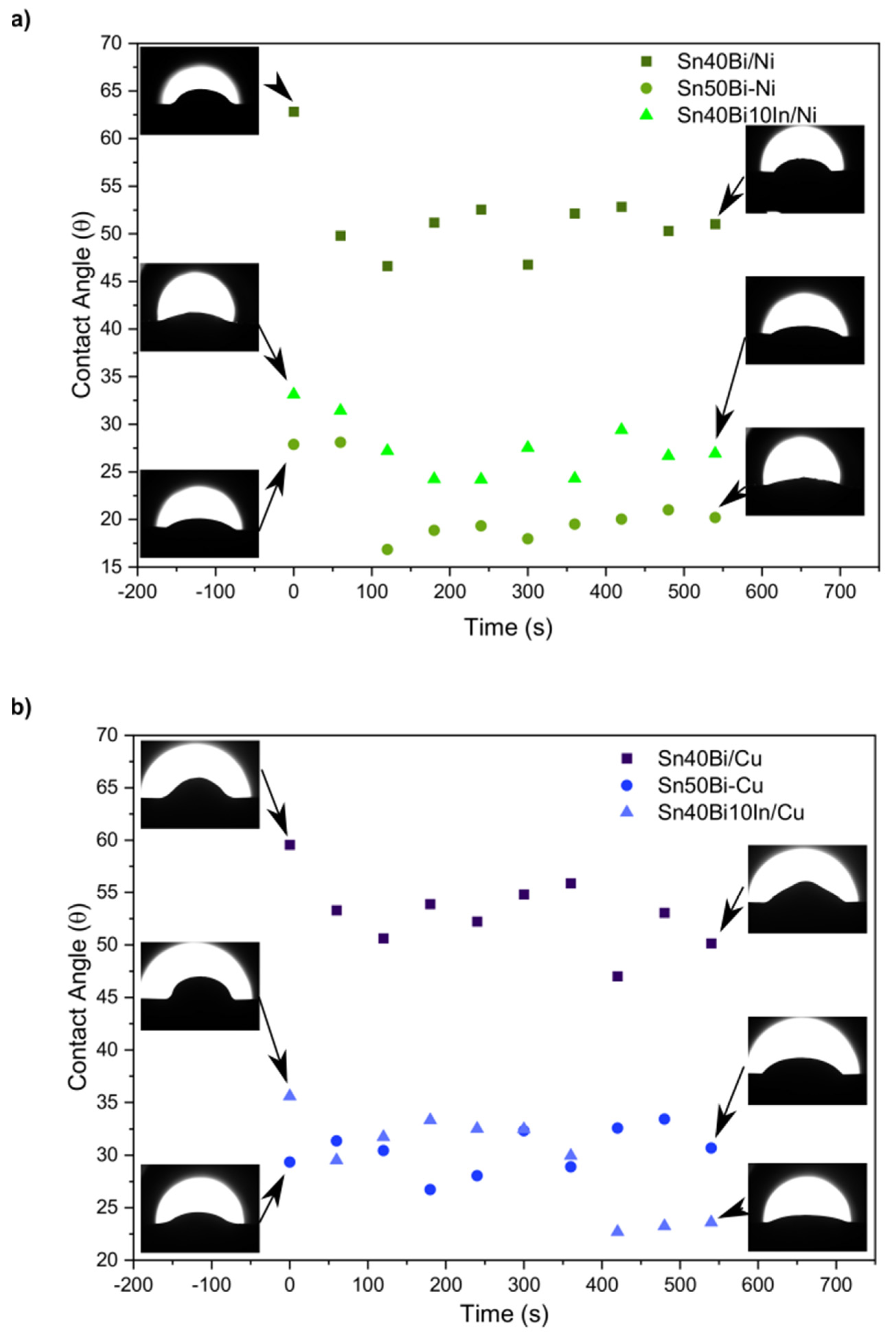
3.2. Wetting Behavior in Copper and Nickel Interfaces

Figure 5 shows the typical wetting angle, θ, profiles obtained as a function of time for the Sn-40%Bi-10%In, Sn-40%Bi, and Sn-50%Bi alloys in copper and nickel surfaces. The Sn-Bi binary alloys have been used as references for comparison with the In-containing samples. Representative images of the contacts for the three alloys Sn-40%Bi, Sn-50%Bi, and Sn-40%Bi-10%In on Cu and Ni substrates are also shown in Figure 5, considering different times from the initial melting state until the stability of θ.
Considering the values after stabilization of the molten drop (i.e., after the initial high contact angles in the first times), average θ values were obtained—45° for the Sn-40%Bi in copper and 53° in nickel, 28° for the Sn-50%Bi in copper and 24° in nickel, and 24 for the Sn-40%Bi-10%In in copper and 26° in nickel—showing that the sample with In resulted in significantly lower θ values. The values obtained for the Sn-50%Bi alloy were close to that for the In samples, as increasing the Bi content tended to improve the fluidity of the alloy [29]. However, a high Bi fraction greatly reduced the alloy ductility, which is detrimental due to the inherent Bi phase brittleness [30]. As the Bi content increased, the melting point of the alloy decreased, and the alloy was more likely to reach overheating at the same testing temperature (i.e., 200 °C), thereby increasing the fluidity and spreading of the alloy.
Nabihah and Naralukmal [9] observed that the addition of In promotes a reduction in the contact angle by decreasing the surface tension of the alloy.
Figure 5. Dynamic change in the contact angles of Sn-40%Bi, Sn-50%Bi, and Sn-40%Bi-10%In on copper and nickel substrates over time, which represents a reactive wetting process and can be divided into three stages: I—θ values immediately upon the alloy are melted, with high contact angles, II—some fluctuation of θ values, and III—the contact angle decreases gradually (data from [31,32]).
Metals 14 00963 g005

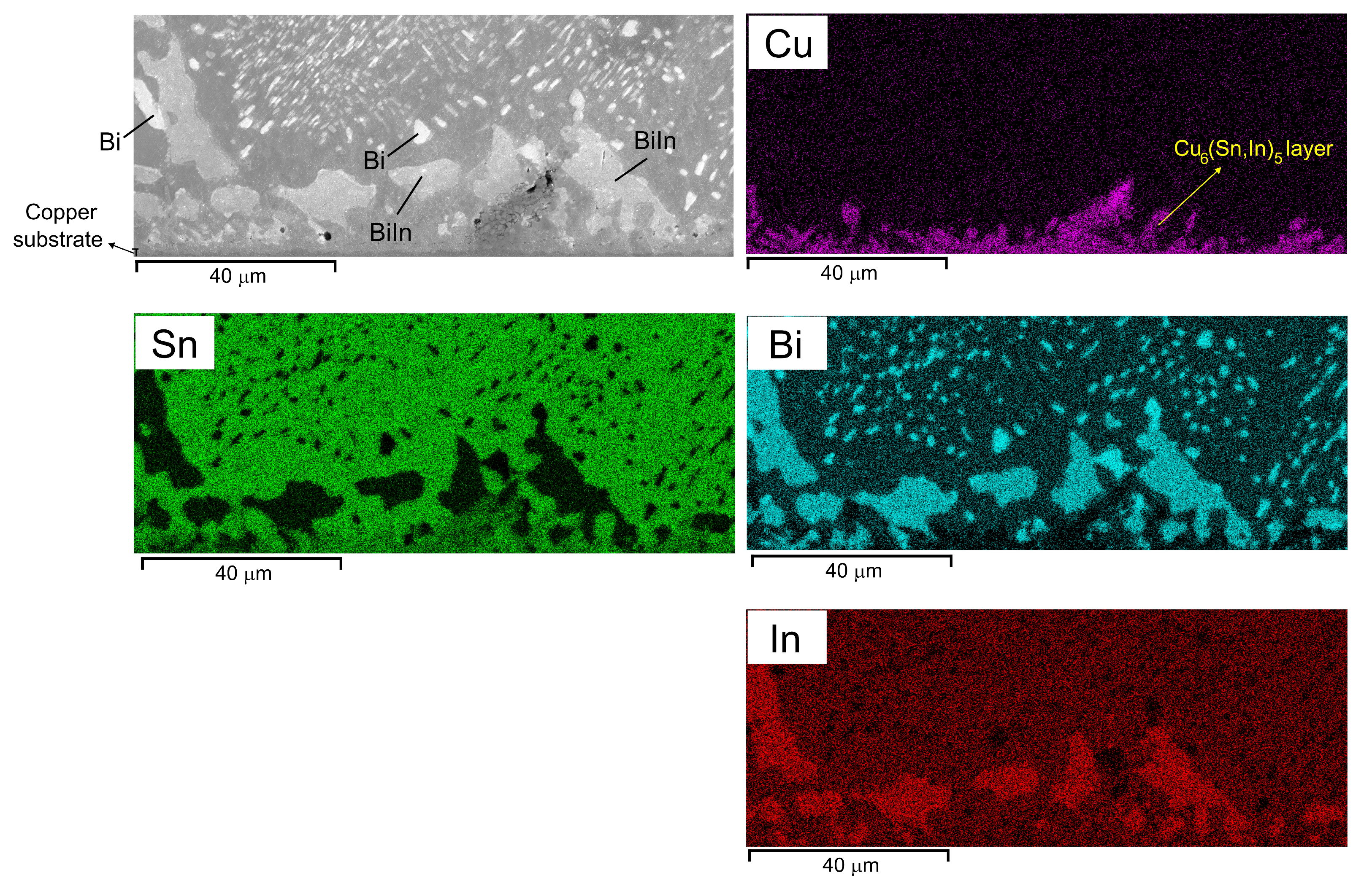
3.3. Interfacial Reaction of the Sn-40%Bi-10%In Samples in Copper

Figure 6 shows the Sn, Cu, Bi, and In maps of regions containing the interfacial Cu6Sn5 in Sn-40%Bi-10%In/Cu. It can be clearly observed that the Cu and Sn distributions are associated with the interfacial IMC layer at the very bottom of the images. Figure 6 shows the phases formed in the alloy and at the interface, as well as the distribution of the elements. The Cu6Sn5 IMC presented a mean solubility of In, approximately 6.5 at.%, as presently determined using point EDS. This value is close to that reported by Tian et al. [33] for the Sn-0.7Cu-5In/copper alloy joints, which was 4.9 at.%. Overall, the composition of this IMC was determined to be 46.5 at.% Sn, 6.5 at.% In, and 47 at.% Cu. This IMC layer is nucleated at the interface because Cu atoms react with the molten solders during the soldering process. Fluxes of tin, copper, and indium atoms also helped the nucleation of Cu6(Sn,In)5; in this condition, these atoms were approached from the solder alloy and the substrate. The size of the IMC is a diffusion-controlled process [34].
In order to understand the growth of the reaction layer after the aging treatment, records of the layers were made for the three occasions at the three temperatures. Figure 7 shows a typical sequence of images for the condition at 120 °C, which express a significant growth of the reaction layer when compared the morphologies among them. The growth of the layer’s size with increasing time was also observed at 100 °C and 110 °C. The nucleation of the IMC layers is defined by the interdiffusion and interfacial reactions. Copper diffuses in the direction of Sn at a higher rate in the inter-diffusion process because copper is a dominant atom with a lower atomic radius than Sn [35]. This assumption was based on marker experiments followed by the Rutherford backscattering spectrometry, which observed that the Cu atoms are the main diffusing species in Sn [36]. Oh et al. [37] later studied the diffusion reactions between Cu/Sn, Cu3Sn/Sn, and Cu/Cu6Sn5. The study showed that both Cu and Sn diffused in CuSn, but the diffusion of Cu was nearly three times faster in CuSn at 200 °C than that of Sn.
A thin IMC layer is desirable for achieving a metallurgical bond, while excess IMCs can weaken the soldered joint. Degradation due to aging is a major concern in electronic junctions, making it essential to understand the kinetics of interfacial reactions. These reactions, driven by atomic diffusion dependent on solidification time, result in IMCs that are prone to structural defects and fragility. Understanding the interactions between the solder alloy and the substrate is essential for forming high-quality solder joints [38]. It can be seen in Figure 7d that longer aging promoted the effective growth of the interfacial intermetallic layer compared to the untreated samples (Figure 7a), as well as compared to the samples exposed to shorter periods (Figure 7b). It is also interesting to note that some needle-shaped Cu6(Sn,In)5 particles were observed not only near the alloy/Cu interface, but also in areas relatively distant from it (particles highlighted with yellow arrows). It seems reasonable to assume that as the temperature dropped during solidification, heterogeneous nucleation at the substrate/alloy interface produced the initial IMCs as part of the layer. The main causes to the formation of some Cu6Sn5 upwards from the pre-existing Cu6Sn5 layer may be nucleation in the liquid away from the reaction layer after a temperature drop or the growth of a particle that detached from the interfacial layer due to convective currents in the liquid. These particles eventually nucleate and grow in the bulk alloy due to the high copper content accumulated in the liquid immediately ahead of the reaction layer. Such accumulation happens due to the surface dissolution of the substrate. Dissolution of Cu to the molten Sn-Cu alloy was also observed by Soares et al. [39]. It was demonstrated that the chemical interaction ahead of the interface is a result of the strong diffusion of Cu from the pads towards the molten alloy, as explained by Laurila et al. [40].
Li et al. [41] observed that copper atoms diffuse through various channels, leading to the formation of Cu6Sn5 particles at the interface. According to the Gibbs–Thomson effect, the smaller Cu6Sn5 IMCs tend to deposit on larger ones because smaller particles have higher solubility [42]. Gagliano and Fine [43] noted that with increased reflow time, Cu6Sn5 undergos coarsening, eventually obstructing the channels between the particles. Some studies have indicated that the growth rate of Cu6Sn5 is controlled by the diffusion and migration velocities of copper atoms, which are influenced by the concentration gradient and the Sn-Cu reaction rate [44].
The development of the IMC’s layer was examined as a function of time, as can be seen in Figure 8a. The kinetics of the IMC layer’s growth is consistently governed by volume diffusion, meaning that the growth rate is always proportional to the time (t). The layer thickness, X, is described by the following equation (Equation (1)):
X = X 0 + D t
where X0 is the thickness of intermetallic layer at t = 0 and D is the diffusion coefficient. When the thickness of the intermetallic layer (X) is plotted against the square root of the aging time (t1/2), the slope of the graph corresponds to the square root of the diffusion coefficient (D1/2), as seen in Figure 8b.
The diffusion coefficient is a function of temperature, T, as expressed by the Arrhenius Equation (2):
D = D 0 e Q R T
where D0 is a temperature-independent constant known as the frequency factor, Q is the activation energy for diffusion, R is the universal gas constant, and T is the absolute temperature in K. The activation energy of the IMC can be determined by taking the natural logarithm of Equation (2). Subsequently, the diffusion coefficient can be represented by Equation (3).
ln D = ln D 0 Q R 1 T
This Equation is in the form y = (m × x) + c, where the dependent variable, y, is lnD and the independent variable, x, is 1/T. By plotting the diffusion coefficient (D) against the inverse of the aging temperature (1/T), the activation energy (Q) can be calculated from the slope of the graph (m), as demonstrated in Figure 8c.
Zang et al. [45] found a growth rate of 5.4 μm/day1/2 for the Cu6Sn5 intermetallic layer in the Sn-45%Bi alloy. Comparing this to the present study, where similar aging treatments were used, the addition of In to the solder reduced the IMC layer’s growth rate from 5.4 μm/day1/2 to 3.3 μm/day1/2, a decrease of approximately 40%. The activation energy of Cu6Sn5 is observed to be lower than that of the Cu6(Sn,In)5. Most of the studies reported activation energy values between 51 kJ/mol and 98 kJ/mol [46,47,48] for the In-free Cu6Sn5 IMC. In sum, one can conclude that the addition of In increases the activation energy needed for the formation of the Cu6Sn5 layer, making the growth of the IMC layer more difficult.

3.4. Adhesion Strength of the Sn-40%Bi-10%In Alloy in Copper and Nickel

Mechanical strength tests were conducted to understand the ability of the joints to withstand mechanical stresses in both nickel and copper substrates. Figure 9 shows the graphs of the tensile tests performed in the solder joints, showing the relationships between load × displacement capacities for the Sn-Bi-In/Ni and the Sn-Bi-In/Cu couples.
The average maximum load values for each sample reached average values of 102 N for the copper substrate and 200 N for the nickel substrate. A projection of the corresponding tensile strengths results in 19 MPa for the alloy/Cu joint and 37 MPa for the alloy/Ni. Wang et al. [49] compared Cu/Sn/Cu and Ni/Sn/Ni solder joints, finding that Ni3Sn4 particles have a more pronounced strengthening effect in the Ni/Sn/Ni joints compared to the Cu6Sn5 particles in the Cu/Sn/Cu joints. Adhesion strength comes mostly from the bonding strength of the IMC/solder interface. So, the maximum adhesion strength may occur in the as-soldered condition in both joints. According to Lee and Chen [50], both the IMC roughness and the fracture mechanism impact the strength. Lee and Chen [50] observed a tensile strength value similar to that found here for the Sn-58%Bi/Cu solder joint reflowed under similar conditions as compared to the procedure adopted here. It was demonstrated that the Bi embrittlement of the Sn-Bi/Cu joint happened due to the diffusion of the Bi atoms from the alloy so that the Bi segregation could be induced. Since these samples were subjected to a non-standardized tensile test, only the maximum adhesion force was considered in this analysis. It was not possible to infer discussions related to the elastic region or initial part of the curves, where one curve for the Cu substrate was above and the other was below the curves related to the Ni substrate.
In addition to the formation of a thinner and less tortuous Ni3Sn4 IMC (Figure 10b), the Sn + Bi eutectic developed to be significantly thinner in the case of the nickel, as seen in Figure 10. The λBi measurements showed a spacing at least three times smaller for the alloy solidified in nickel. This indicates a fast cooling associated with nickel. Moreover, finer Bi may induce higher joint strength.
The IMC layer formed at the interface of the alloy/substrate couple is the most critical region of the solder joint, as this is where structural defects tend to nucleate. During soldering, the alloy reacts with the substrate, resulting in the formation of a complex IMC layer. Creating a soldered joint involves various intricate metallurgical processes, including heat and mass transfer. It is worth noting that the heat transfer efficiency between the alloy and the substrate can be affected by the level of wettability between the two parts. In turn, the heat flux through the solder’s alloy/substrate interface contributes directly on the evolution of solidification, i.e., it affects the final microstructure of the soldered joints [39]. When a molten solder and substrate’s surfaces are brought into contact, an imperfect junction is formed. Silva et al. [32] highlighted that the junction’s effectiveness is influenced by the alloy’s thermophysical properties, substrate roughness, melting superheat, freezing range, and wetting behavior. Heat transfer efficiency is a key factor in controlling the solidification and microstructure’s evolution.
Although copper has higher thermal conductivity than nickel [51], and both substrates showed very similar wettability when compared (see Figure 5), voids were detected at the alloy’s boundaries for the copper substrate (blue arrows in Figure 10) but not for the nickel substrate. According to Soares et al. [39], these voids counteract the high thermal conductivity of copper so that overall heat flow decreased. As such, a coarser eutectic was formed in the alloy solidified in copper (Figure 10a).
In both substrates, the fracture predominantly occurred at the boundary between the alloy and the IMC. The fracture surfaces of the Sn-Bi-In/Ni and Sn-Bi-In/Cu joints in both the alloy’s fracture plane and the IMC layer’s plane were analyzed to understand the fracture mode that occurred. Solder joints with higher IMC thickness, rough morphology, and coarser microstructure characterized the Sn-Bi-In/copper joints, resulting in lower resistance values being observed.
A typical ductile fracture morphology can be observed, characterized by the predominance of small and big dimples (indicated by arrows in Figure 11), with the larger dimples formed by the coalescence of smaller ones. The phases present at the fracture’s interface were also confirmed, particularly the Bi, the Cu6(Sn,In)5, and Ni3Sn4 IMCs. Some cleavage planes, likely originated from the brittle Bi phase, were also observed. In the case of the alloy/copper joint in the IMC fracture plane (Figure 11b,d), the dimples were notably larger, which might have led to premature failure.
Figure 12 shows high-magnification fractography images of the two alloy/copper and alloy/nickel joints. It is possible to confirm the presence of dimpled fracture morphology, where dimples coalesce to form deeper voids and observe regions with cleavage features associated with Bi. The Cu6Sn5 IMCs are clearly visible from the fracture plane in Figure 12a, whereas the observation of the Ni3Sn4 IMCs is less clear in Figure 12b. For the fracture interface on the alloy’s side plane, both small and large dimples are visible, along with Bi regions exhibiting cleavage features.

4. Conclusions

The following conclusions can be drawn from the present research:
-
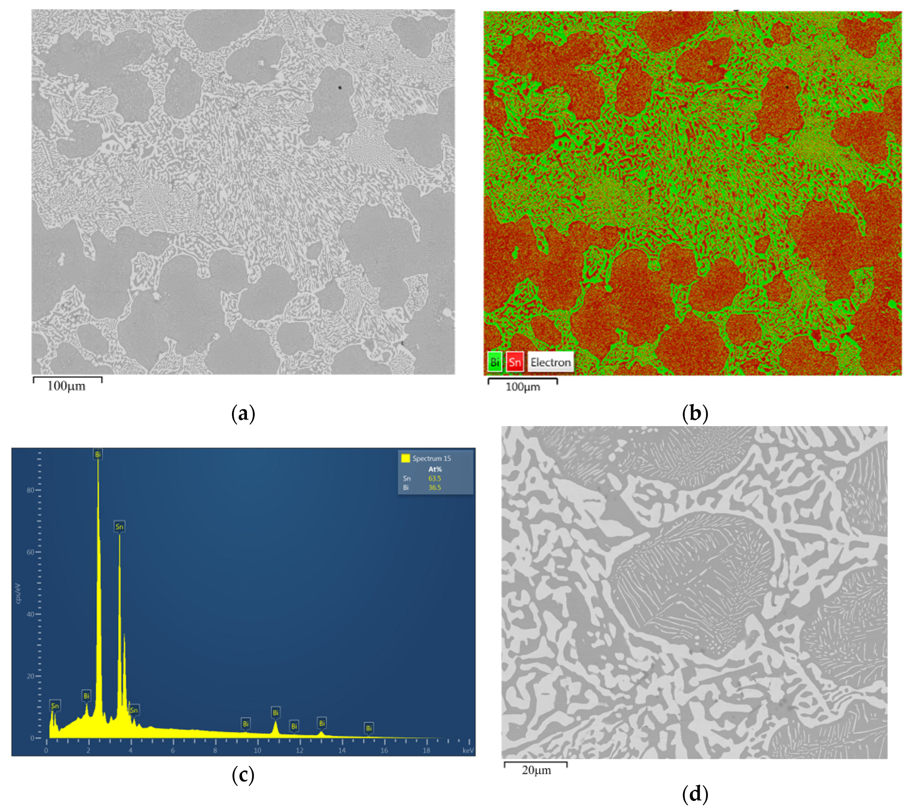
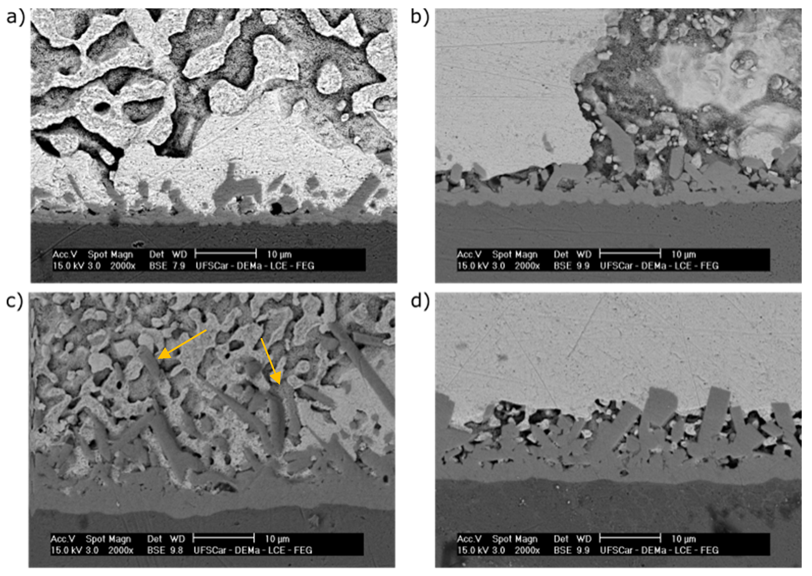
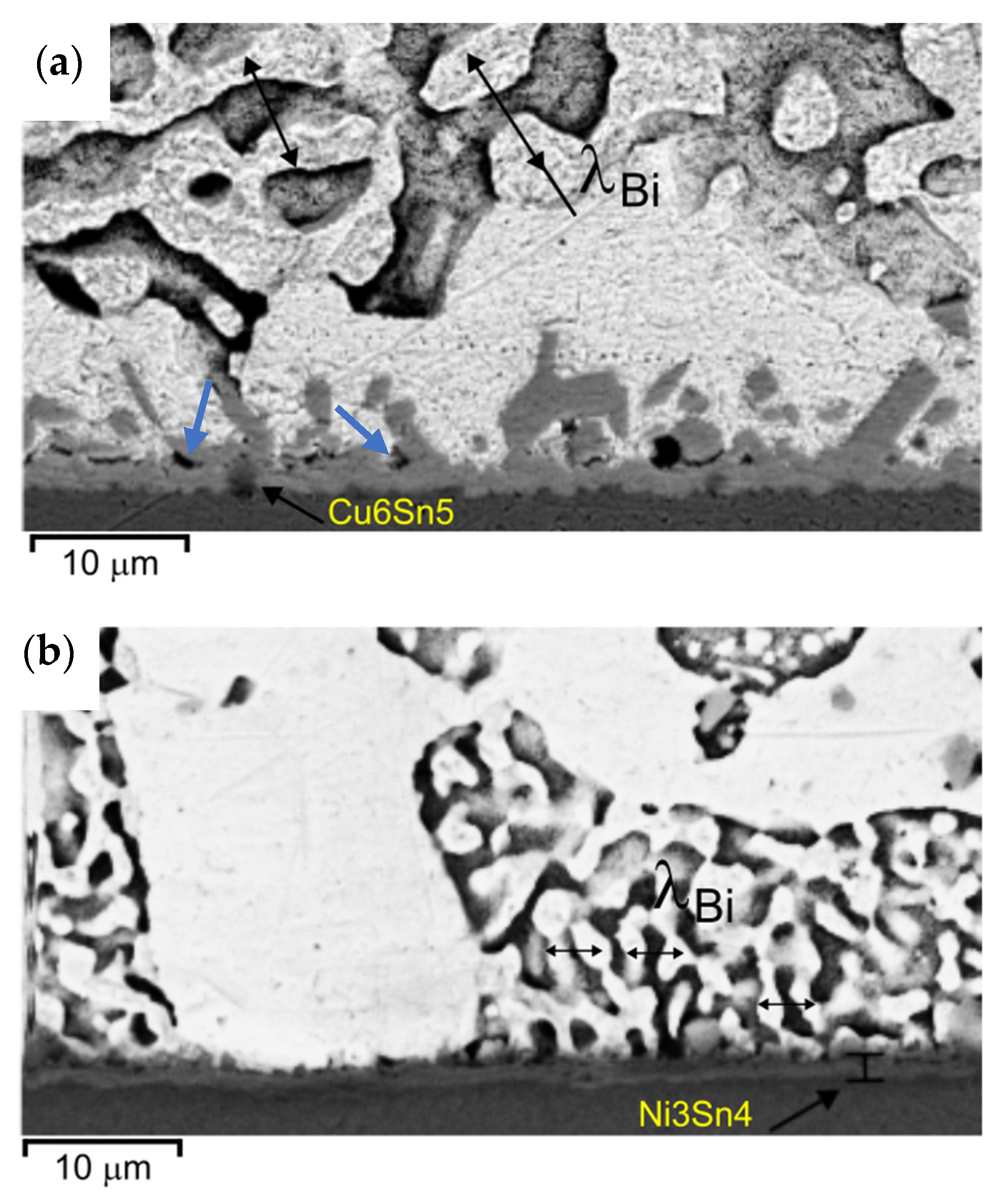
Significant macrosegregation of Bi towards the Cu/alloy interface in both Sn-40%Bi and Sn-40%Bi-10%In alloys was observed, with the latter showing the formation of coarse Bi and a more pronounced segregation pattern. This segregation aligns with previous findings that higher Bi content results in thicker IMC layers.
-
Both alloys exhibited β-Sn dendritic primary phases, with Bi forming in eutectic-like morphologies in the ternary alloy (Sn-40%Bi-10%In) and as a final eutectic reaction in the binary alloy (Sn-40%Bi).
-
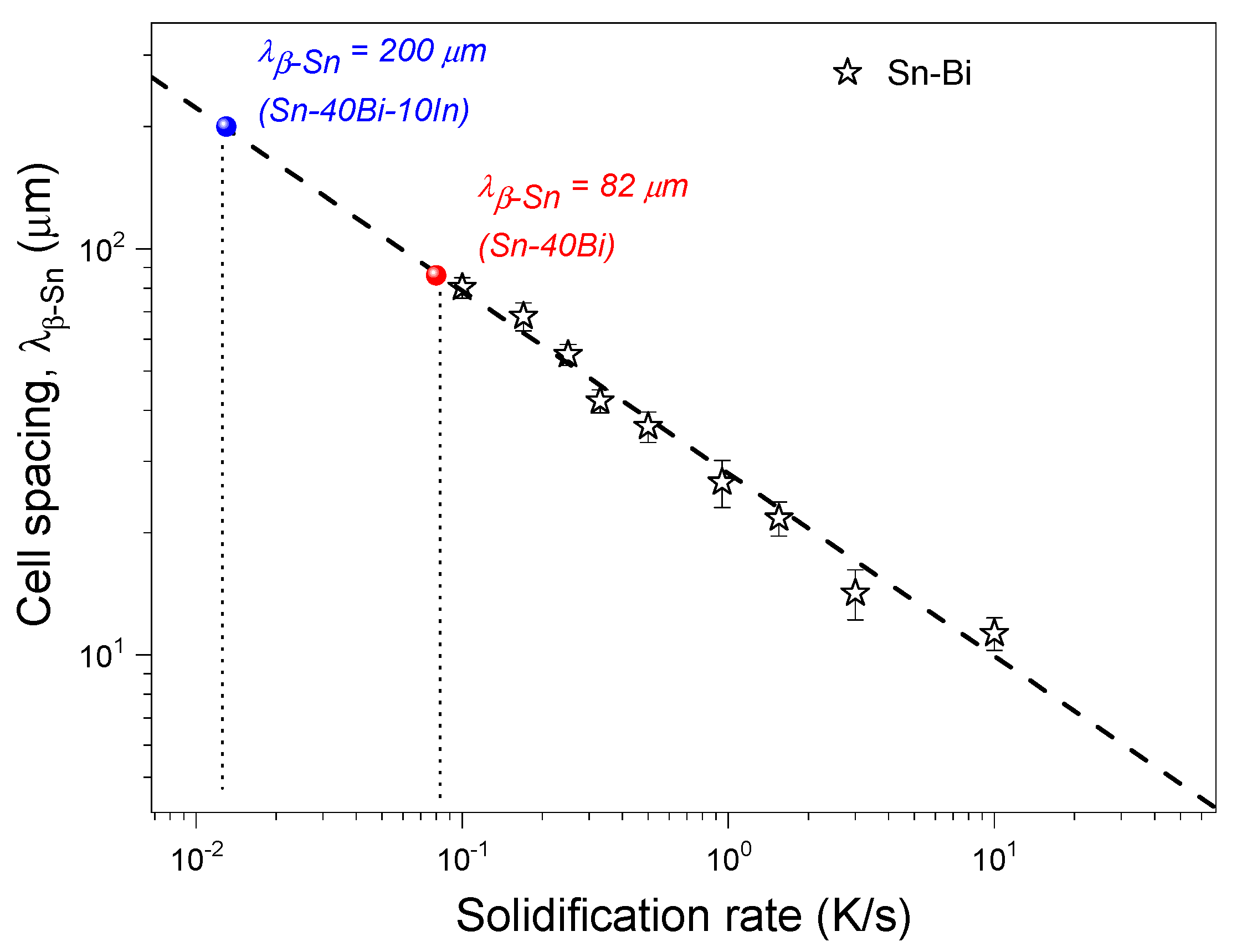
The Sn-40%Bi-10%In alloy demonstrated a larger cell spacing (200 μm) as compared to the binary Sn-40%Bi alloy, which had a spacing of 82 μm. The presence of In significantly influenced the cell and Bi spacing, resulting in approximately three times coarser structures due to the extended solidification interval.
-
The Sn-40%Bi-10%In/Cu joint exhibited the formation of Cu6(Sn,In)5 IMCs, with In incorporation leading to a reduction in IMC layer growth rate by 40% compared to the Sn-40%Bi alloy. The addition of In increased the activation energy needed for the formation of the Cu6Sn5 layer, making its growth more difficult. Adhesion strength tests indicated slightly higher adhesion strength in the Sn-Bi-In/Ni joints (37 MPa) compared to the Sn-Bi-In/Cu joints (19 MPa), which is attributed to the finer microstructure and less tortuous IMC layer formed in the contact with nickel. The fracture predominantly occurred at the alloy/IMC boundary, with dimples and cleavage features observed in the fracture’s surface.

Author Contributions

Methodology, J.R.d.S.L., R.A.V.R. and G.L.d.G.; formal analysis, J.R.d.S.L., J.E.S. and F.G.C.; investigation, J.R.d.S.L. and J.E.S.; resources, J.E.S.; data curation, G.L.d.G., R.A.V.R. and J.R.d.S.L.; writing, J.E.S. and J.R.d.S.L., writing—review and editing, J.E.S. and F.G.C.; visualization, J.E.S. and J.R.d.S.L.; supervision, J.E.S. and F.G.C.; project administration, J.E.S.; funding acquisition, J.E.S. All authors have read and agreed to the published version of the manuscript.

Funding

The authors are grateful to CNPq—National Council for Scientific and Technological Development, Brazil and to FAPESP—São Paulo Research Foundation, Brazil (grant 2023/06107-3) for their financial support. This study was financed in part by the Coordenação de Aperfeiçoamento de Pessoal de Nível Superior—Brasil (CAPES)—Finance Code 001.

Data Availability Statement

The data presented in this study are available upon request from the corresponding author. They are not publicly accessible because the research is still ongoing.

Acknowledgments

We thank the Laboratory of Structural Characterization, Department of Materials Engineering, Federal University of São Carlos, for use of its SEM facilities.

Conflicts of Interest

The authors declare no conflicts of interest.

References

  1. Zhang, W.; Zhao, J.; Yin, Z.; Zhou, N.; Tang, L.; Suo, C. Study on wettability of low-melting alloy material on copper substrates. Ferroelectrics 2019, 549, 160–171. [Google Scholar] [CrossRef]
  2. Roy, C.K.; Bhavnani, S.; Hamilton, M.; Johnson, W.R.; Knight, R.W.; Harris, D.K. Performance of Low Melt Alloys as Thermal Interface Materials. In Proceedings of the 2015 31st Thermal Measurement, Modeling & Management Symposium (SEMI-THERM), San Jose, CA, USA, 15–19 March 2015. [Google Scholar]
  3. Cheng, S.; Huang, C.; Pecht, M. A review of lead-free solders for electronics applications. Microelectron. Reliab. 2017, 75, 77–95. [Google Scholar] [CrossRef]
  4. Kurz, W.; Fisher, D.J. Fundamentals of Solidification. Trans. Tech. Public. 1992, 87. [Google Scholar]
  5. Wu, X.; Wu, J.; Wang, X.; Yang, J.; Xia, M.; Liu, B. Effect of In addition on microstructure and mechanical properties of Sn–40Bi alloys. J. Mater. Sci. 2020, 55, 3092–3106. [Google Scholar] [CrossRef]
  6. Goh, Y.; Haseeb, A.S.M.A.; Sabri, M.F.M. Effects of hydroquinone and gelatin on the electrodeposition of Sn-Bi low temperature Pb-free solder. Electrochim. Acta 2013, 90, 265–273. [Google Scholar] [CrossRef]
  7. Shen, C.; Hai, Z.; Zhao, C.; Zhang, J.; Evans, J.L.; Bozack, M.J.; Suhling, J.C. Packaging Reliability Effect of ENIG and ENEPIG Surface Finishes in Board Level Thermal Test under Long-Term Aging and Cycling. Materials 2017, 10, 451. [Google Scholar] [CrossRef]
  8. Spinelli, J.E.; Cheung, N.; Goulart, P.R.; Quaresma, J.M.V.; Garcia, A. Design of mechanical properties of Al-alloys chill castings based on the metal/mold interfacial heat transfer coefficient. Int. J. Therm. Sci. 2012, 51, 145. [Google Scholar] [CrossRef]
  9. Nabihah, A.; Nurulakmal, M.S. Effect of In Addition on Microstructure, Wettability and Strength of SnCu Solder. Mater. Today Proc. 2019, 17, 803–809. [Google Scholar] [CrossRef]
  10. Silva, B.L.; Bertelli, F.; Cante, M.V.; Spinelli, J.E.; Cheung, N.; Garcia, A. Solder/substrate interfacial thermal conductance and wetting angles of Bi–Ag solder alloys. J. Mater. Sci. Mater. Electron. 2016, 27, 1994. [Google Scholar] [CrossRef]
  11. Li, Q.; Ma, N.; Lei, Y.; Lin, J.; Fu, H.; Gu, J. Characterization of Low-Melting-Point Sn-Bi-In Lead-Free Solders. J. Electron. Mater. 2016, 45, 5800–5810. [Google Scholar] [CrossRef]
  12. Vianco, P.T.; Rejent, J.A.; Hlava, P.F. Solid-state intermetallics compound layer growth between copper and 95.5Sn-3.9Ag-0.6Cu solder. J. Electron. Mater. 2004, 33, 991–1004. [Google Scholar] [CrossRef]
  13. Lee, T.Y.; Choi, W.J.; Tu, K.N.; Jang, J.W.; Kuo, S.M.; Lin, J.K.; Frear, D.R.; Zeng, K.; Kivilahti, J.K. Morphology, kinetics, and thermodynamics of solid-state aging of eutectic SnPb and Pb-free solders (Sn-3.5Ag, Sn-3.8Ag-0.7Cu and Sn-0.7Cu) on Cu. J. Mater. Res. 2002, 17, 291–301. [Google Scholar] [CrossRef]
  14. Gómez, M.; Xu, G.; Li, J.; Zeng, X. Securing Indium Utilization for High-Tech and Renewable Energy Industries. Environ. Sci. Technol. 2023, 57, 2611–2624. [Google Scholar] [CrossRef] [PubMed]
  15. Zhang, Y.; Kim, M.; Wang, L.; Verlinden, P.; Hallam, B. Design considerations for multi-terawatt scale manufacturing of existing and future photovoltaic technologies: Challenges and opportunities related to silver, indium and bismuth consumption. Energy Environ. Sci. 2021, 14, 5587–5610. [Google Scholar] [CrossRef]
  16. Prakash, A.; Byrd, K.; Sidhu, R.; Elhalawaty, S.; Wu, N.; Okumura, H.; Erukula, S.; Lim, J. Challenges and key learnings in enabling Low Temperature Solder (LTS) technology at packaging components supply base. In Proceedings of the 2021 IEEE 71st Electronic Components and Technology Conference (ECTC), San Diego, CA, USA, 1 June–4 July 2021; pp. 635–642. [Google Scholar] [CrossRef]
  17. Wang, F.; Huang, Y.; Zhang, Z.; Yan, C. Interfacial Reaction and Mechanical Properties of Sn-Bi Solder joints. Materials 2017, 10, 920. [Google Scholar]
  18. Yoon, S.W.; Rho, B.; Lee, H.M.; Kim, C.; Lee, B.J. Investigation of the phase equilibria in the Sn-Bi-In alloy system. Metall. Mater. Trans. A 1999, 30, 1503. [Google Scholar] [CrossRef]
  19. Manasijević, I. Study of microstructure and thermal properties of the low melting Bi-In-Sn eutectic alloys. Mater. Res. 2018, 21, e20180501. [Google Scholar] [CrossRef]
  20. Leal, J.R.; Reyes, R.A.V.; de Gouveia, G.L.; Coury, F.G.; Spinelli, J.E. Effects of Indium on Wetting and Interfacial Features of a Sn-40Bi Alloy in a Copper Substrate. J. Electron. Mater. 2023, 52, 2957–2970. [Google Scholar] [CrossRef]
  21. Dong Mj Gao, Z.; Liu, Y.; Wang, X.; Yu, L.M. Effect of indium addition on the microstructural formation and soldered interfaces of Sn-2.5Bi-1Zn-0.3Ag lead-free solder. Int. J. Miner. Metall. Mater. 2012, 19, 1029–1035. [Google Scholar] [CrossRef]
  22. Silva, B.; Silva, V.C.; Garcia, A.; Spinelli, J.E. Effects of solidification thermal parameters on microstructure and mechanical properties of Sn-Bi solder alloys. J. Electron. Mater. 2017, 46, 1754–1769. [Google Scholar] [CrossRef]
  23. Glazer, J. Metallurgy of low temperature Pb-free solders for electronic assembly. Inter. Mater. Rev. 1995, 40, 65. [Google Scholar] [CrossRef]
  24. Li, J.F.; Mannan, S.H.; Clode, M.P.; Whalley, D.C.; Hutt, D.A. Interfacial reactions between molten Sn-Bi-X solders and Cu substrates for liquid solder interconnects. Acta Mater. 2006, 54, 2907. [Google Scholar] [CrossRef]
  25. Torres, A.; Hernández, L.; Domínguez, O. Effect of antimony additions on corrosion and mechanical properties of Sn-Bi eutectic lead-free solder alloy. Mater. Sci. Appl. 2012, 3, 355–362. [Google Scholar] [CrossRef]
  26. Wu, J.A.; Luktuke, A.; Chawla, N. Surface Precipitation and Growth of Bismuth Particles in Sn-Ag-Cu-Bi Solder Joints. J. Electron. Mater. 2023, 52, 801–809. [Google Scholar] [CrossRef]
  27. Wang, F.; Luktuke, A.; Chawla, N. Microstructural coarsening and mechanical properties of eutectic Sn-58Bi solder joint during aging. J. Electron. Mater. 2021, 50, 6607. [Google Scholar] [CrossRef]
  28. Spinelli, J.E.; Leal, J.R.; Wu, J.A.; Luktuke, A.; Ganju, E.; Chawla, N. Long-Term Microstructural Stability of Sn-40Bi and Sn-40Bi-10In Alloys. J. Electron. Mater. 2024, 53, 2455–2466. [Google Scholar] [CrossRef]
  29. Pu, C.; Qiu, J.; Li, C.; Gao, P.; Peng, Y.; He, Q.; Bai, H.; Yi, J. Effects of Bi Addition on the Solderability and Mechanical Properties of Sn-Zn-Cu Lead-Free Solder. J. Electron. Mater. 2022, 51, 4952–4963. [Google Scholar] [CrossRef]
  30. Erer, A.M.; Oguz, S.; Türen, Y. Influence of bismuth (Bi) addition on wetting characteristics of Sn-3Ag-0.5Cu solder alloy on Cu substrate. Eng. Sci. Technol. Int. J. 2018, 21, 1159–1163. [Google Scholar] [CrossRef]
  31. Zhang, X.; Yuan, Z.; Zhao, H.; Zang, L.; Li, J. Wetting behavior and interfacial characteristic of Sn–Ag–Cu solder alloy on Cu substrate. Phys. Chem. 2010, 55, 797–801. [Google Scholar] [CrossRef]
  32. Silva, B.L.; Cheung, N.; Garcia, A.; Spinelli, J.E. Evaluation of solder/substrate thermal conductance and wetting angle of Sn–0.7wt%Cu–(0–0.1wt%Ni) solder alloys. Mater. Lett. 2015, 142, 163–167. [Google Scholar] [CrossRef]
  33. Tian, S.; Li, S.; Zhou, J. Effect of indium addition on interfacial IMC growth and bending properties of eutectic Sn–0.7Cu solder joints. J. Mater. Sci. Mater. Electron. 2017, 28, 16120. [Google Scholar] [CrossRef]
  34. Wang, Y.; Yao, Y.; Keer, L. An analytical model to predict diffusion induced intermetallic compounds growth in Cu-Sn-Cu sandwich structures. Theor. Appl. Mech. Lett. 2020, 10, 33–37. [Google Scholar] [CrossRef]
  35. Kannojia, H.K.; Dixit, P. A review of intermetallic compound growth and void formation in electrodeposited Cu–Sn Layers for microsystems packaging. J. Mater. Sci. Mater. Electron. 2021, 32, 6742–6777. [Google Scholar] [CrossRef]
  36. Tu, K.N.; Thompson, R.D. Kinetics of interfacial reaction in bimetallic CuSn thin films. Acta Metall. 1982, 30, 947–952. [Google Scholar] [CrossRef]
  37. Oh, M. Growth Kinetics of Intermetallic Phases in the Cu-Sn Binary and the Cu-Ni-Sn Ternary Systems at Low Temperatures; Lehigh University: Bethlehem, PA, USA, 1994. [Google Scholar]
  38. Lee, T.K.; Bieler, T.R.; Kim, C.U.; Ma, H. Fundamentals of Lead-Free Solder Interconnect Technology: From Microstructures to Reliability, 1st ed.; Springer: New York, NY, USA, 2015. [Google Scholar]
  39. Soares, T.; Cruz, C.; Silva, B.; Brito, C.; Garcia, A.; Spinelli, J.E.; Cheung, N. Interplay of Wettability, Interfacial Reaction and Interfacial Thermal Conductance in Sn-0.7Cu Solder Alloy/Substrate Couples. J. Electron. Mater. 2020, 49, 173–187. [Google Scholar] [CrossRef]
  40. Laurila, T.; Hurtig, J.; Vuorinen, V.; Kivilahti, J.K. Effect of Ag, Fe, Au and Ni on the growth kinetics of Sn–Cu intermetallic compound layers Microelectron. Reliab. 2009, 49, 242. [Google Scholar] [CrossRef]
  41. Li, Z.H.; Tang, Y.; Guo, Q.W.; Li, G.Y. A diffusion model and growth kinetics of interfacial intermetallic joints. J. Alloys Compd. 2020, 818, 152893. [Google Scholar] [CrossRef]
  42. Ely, D.R.; García, R.E.; Thommes, M. Ostwalde-Freundlich diffusion-limited dissolution kinetics of nanoparticles. Powder Technol. 2014, 257, 120–123. [Google Scholar] [CrossRef]
  43. Gagliano, R.A.; Fine, M.E. Growth of η phase scallops and whiskers in liquid tin-solid copper reaction couples. J. Miner. 2001, 53, 33–38. [Google Scholar] [CrossRef]
  44. Mei, Z.; Sunwoo, A.J.; Morris, J.W. Analysis of low-temperature intermetallic growth in copper-tin diffusion couples. Metall. Mater. Trans. A 1992, 23, 857–864. [Google Scholar] [CrossRef]
  45. Zang, L.; Yuan, Z.; Zhao, H.; Zhang, X. Wettability of molten Sn-Bi-Cu solder on Cu substrate. Mater. Lett. 2009, 63, 2067–2069. [Google Scholar] [CrossRef]
  46. Prakash, K.H.; Sritharan, T. Interface reaction between copper and molten tin-lead solders. Acta Mater. 2001, 49, 2481–2489. [Google Scholar] [CrossRef]
  47. Shewmon, P. Diffusion in Solids; TMS: Warrendale, PA, USA, 1989; pp. 191–202. [Google Scholar]
  48. Mookam, N.; Kanlayasiri, K. Evolution of intermetallic compounds between Sn-0.3Ag-0.7Cu low-silver lead-free solder and Cu substrate during thermal aging. J. Mater. Sci. Technol. 2012, 28, 53–59. [Google Scholar] [CrossRef]
  49. Wang, B.; Wu, F.; Wu, Y.; An, B.; Liu, H.; Zou, J. A comparative study of microstructure and mechanical properties among Cu/Sn/Cu, Ni/Sn/Ni and Cu/Sn/Ni solder joints. Solder. Surf. Mt. Technol. 2011, 23, 40–46. [Google Scholar] [CrossRef]
  50. Lee, H.T.; Chen, M.H. Influence of intermetallic compounds on the adhesive strength of solder joints. Mater. Sci. Eng. A 2002, 333, 24–34. [Google Scholar] [CrossRef]
  51. MatWeb: Online Materials Information Resource. Available online: http://www.matweb.com/ (accessed on 5 January 2024).
Figure 1. SEM images of the as-soldered (a) Sn-40%Bi-10%In and (b) Sn-40%Bi alloys from the bottom to the top of the joints with copper.
Metals 14 00963 g001
Figure 2. β-Sn cell spacing as a function of the solidification cooling rate; blue and red points for the Sn-40%Bi-10%In and Sn-40%Bi alloys, respectively, were obtained through extrapolation of the experimental equation for the Sn-Bi alloy demonstrated by Silva et al. Dashed line from ref. [22].
Metals 14 00963 g002
Figure 3. SEM-EDS dot-map analysis for the Sn-40%Bi-10%In: (a) SEM image, (b) Sn, (c) Bi, (d) In, and (e) corresponding ED spectrum.
Metals 14 00963 g003
Figure 4. SEM-EDS dot-map analysis for the Sn-40%Bi alloy: (a) SEM image, (b) Sn and Bi contrasts, (c) corresponding ED spectrum, and (d) high-magnification SEM image highlighting the Bi precipitates.
Metals 14 00963 g004
Figure 6. Backscattered SEM image and EDS mapping images of the interfacial Cu6Sn5 IMC layer of Sn-40%Bi-10%In/Cu taken subsequent to the soldering process.
Metals 14 00963 g006
Figure 7. Morphologies of IMC layers aged at 120 °C for the Sn-40%Bi-10%In/copper couple: (a) as soldered, (b) 5 days (120 h), (c) 10 days (240 h), and (d) 15 days (360 h).
Metals 14 00963 g007
Figure 8. (a) Average thickness of the Cu6Sn5 IMC layer of the Sn-40%Bi-10% alloy in copper solder at the different aging times, (b) IMC thickness against the square root of time, and (c) Arrhenius plot for the growth of the IMC layer. R2 is the correlation coefficient.
Metals 14 00963 g008
Figure 9. Load vs. displacement curves for the untreated Sn-Bi-In/copper and Sn-Bi-In/nickel solder joints.
Metals 14 00963 g009
Figure 10. SEM images showing the details of the IMCs formed during soldering of the Sn-40%Bi-10%In alloy in (a) copper and (b) nickel.
Metals 14 00963 g010
Figure 11. Fracture surfaces of the Sn-Bi-In/Cu and Sn-Bi-In/Ni joints reflowed at 220 °C: (a) alloy/IMC in copper (view of the alloy fracture plane), (b) alloy/IMC in copper (view of the fracture plane of the IMC layer), (c) alloy/IMC in nickel (view of the alloy fracture plane), and (d) alloy/IMC in nickel (view of the fracture plane of the IMC layer).
Metals 14 00963 g011
Figure 12. Details of the fracture surfaces in high magnification: Sn-Bi-In/IMC in (a) copper and (b) nickel (view of the fracture plane of the IMC layer), and in (c) copper and (d) nickel with the view of the alloy’s side plane.
Metals 14 00963 g012
Disclaimer/Publisher’s Note: The statements, opinions and data contained in all publications are solely those of the individual author(s) and contributor(s) and not of MDPI and/or the editor(s). MDPI and/or the editor(s) disclaim responsibility for any injury to people or property resulting from any ideas, methods, instructions or products referred to in the content.

