Article

Comparative Studies of the Properties of Copper Components: Conventional vs. Additive Manufacturing Technologies

by
Witold Malec
1,
Joanna Kulasa
1,
Anna Brudny
1,
Anna Hury
1,
Bartlomiej Adamczyk
2,
Ryszard Rzepecki
2,
Robert Sekula
3,
Grzegorz Kmita
3 and
Andrzej Rybak
2,*
1
Łukasiewicz Research Network—Institute of Non-Ferrous Metals, Sowinskiego 5, 44-121 Gliwice, Poland
2
ABB Corporate Technology Center, Starowislna 13A, 31-038 Krakow, Poland
3
Hitachi Energy Research, Pawia 7, 31-154 Krakow, Poland
*
Author to whom correspondence should be addressed.
Metals 2024, 14(9), 975; https://doi.org/10.3390/met14090975
Submission received: 28 June 2024 / Revised: 13 August 2024 / Accepted: 25 August 2024 / Published: 28 August 2024
(This article belongs to the Special Issue Advances in 3D Printing Technologies of Metals—2nd Edition)

Abstract

:
This article presents a comparative analysis of the crucial physical properties of electrically conductive components made of pure copper, produced by various additive manufacturing technologies such as binder jetting (BJ) and direct metal laser sintering (DMLS). The comparison concerned the assessment of critical parameters important from the application point of view, such as: electrical conductivity, hardness, yield point, microstructure and the occurrence of internal material defects. Same-sized components made in a conventional casting and subtractive method (machining) were used as a reference material. Comprehensive tests and the comparison of a wide range of parameters allowed us to determine that among the selected methods, printing using the DMLS technique allowed for obtaining arcing contact with mechanical and electrical parameters very similar to the reference element. Therefore, the obtained results showed the possibility of using the copper elements made by additive manufacturing for the switching and protection devices used in electrification and energy distribution industrial sectors.

1. Introduction

The use of pure copper and its alloys in the production of components by additive manufacturing is relatively rare due to the specificity of the application and the resulting set of requirements that must be met. This is mainly because of the high electrical and thermal conductivity and good corrosion resistance, since the use of copper is very often limited to applications where a high electrical current density (e.g., contact elements for switching and protection devices, like circuit breakers) and/or high heat conductivity are required (e.g., heat sinks, heat pipes) [1,2,3,4,5,6]. Since additive manufacturing provides almost unlimited freedom of design and optimization, components produced from pure copper in related technologies have great potential for use wherever single pieces with unique shapes or even short series are needed. Applications in such areas as power and electrification products, electronics, the automotive industry, the aviation industry, as well as in heat management systems and others, in which components are traditionally produced by methods based on subtractive manufacturing (SM) or by sand casting (SC), can be mentioned here. However, the production of copper components by sand casting is economically limited to large production quantities, so in fact the only method to cost-effectively produce single components is the subtractive approach [7,8].
Conventional production of components by machining is associated with high material and labour consumption, and thus high costs and a long production time. In addition, machining of copper can cause problems related to its low machinability. In the case of casting, there are advantages in the possibility of precise selection of the batch material with the desired properties, and good precision of manufacturing. On the other hand, the main obstacle with casting is the need to prepare the model necessary to make the mould in the moulding sand beforehand. In this regard, the use of 3D printing to produce a complete mould from moulding sand seems to be a major convenience. The advantage of casting is a relatively good representation of the shape of the desired element, especially if it is necessary to obtain better tolerances and surface quality, as well as precise mapping of certain shapes, such as e.g., holes. Thus, the machining of the pre-cast features, such as holes and undercuts, is more material-saving and thus simpler and cheaper.
However, the development of new printing technologies has created completely new possibilities and allowed for significant progress in this area, not only for polymers but also for metal products. The practical application of additive technologies in industry has already become a fact in many industries and in a wide range of manufacturing technologies [9]. There are known achievements concerning the production of components made of materials such as stainless steel, tool steel, aluminium alloys, titanium and titanium alloys, Inconel, nickel alloys (superalloys), magnesium alloys, ceramic matrix composites, as well as noble alloys, copper, and copper alloys [10,11,12,13,14,15]. However, many of the developed additive technologies have been referred to by different names, creating a certain terminological disorder, which was largely unified by the standard [16], on which the presented description is based.
Pure copper is quite a demanding material in terms of additive manufacturing due to certain limitations caused by its material properties. The first problem is the high thermal conductivity of copper, which during the printing process leads to a rapid heat evacuation from the melting area, causing high temperature gradients; this, consequently, can lead to delamination of the deposited layers, curling of the material and damage to the formed element. Another limitation is the high plasticity of copper, which makes it difficult to remove and to recover the copper powder after building subsequent layers of the element. In addition, the copper powder particles tend to agglomerate, which also has a negative effect on the 3D printing process by changing the flowability of the material, which determines the quantity and quality of the deposited material. In addition, copper is susceptible to surface oxidation, which requires special storage of the material before use, as well as protection during the process (the process is carried out in a non-oxidizing atmosphere) [17,18,19]. Taking these obstacles into consideration, the most promising printing technologies that can compete with traditional technologies are binder jetting, or powder sintering/melting with a laser or electron beam (EBM).
Moreover, new AM technologies were developed long enough ago to become an equivalent production method today. This also applies to copper products, for which the manufacturing using AM technologies (in particular Powder Bed Fusion) has become a fully mastered process, despite significant difficulties with this material due to its very good thermal conductivity and high reflectance, which makes it difficult to use, especially with laser-based technologies.
A review of the literature has shown that it is difficult to find research works that, in a complementary way, compare a wide range of functional parameters of elements obtained from pure copper using different methods, ranging from mechanical processing, through casting, to 3D printing. Therefore, the aim of the presented research was to perform a detailed and complementary research in order to compare the crucial properties of small-size components made of pure copper with the use of various AM technologies with the properties of the same elements obtained using traditional methods. An analysis was carried out to compare the set of critical parameters important from the application point of view, such as electrical conductivity, hardness, yield point, plasticity, as well as microstructure analysis, in order to evaluate the occurrence of internal material defects. Printed components were produced using binder jetting (BJ) [20] and direct metal laser sintering (DMLS) [21] methods, which are widely used for copper printing. Same-sized components made in the traditional way by sand casting and subtractive manufacturing (cutting/machining) were used as reference materials. The obtained results allowed for the assessment of the possibility of using 3D printed copper elements for the switching and protection devices used in the area of electrification, where the rated operational voltage and current are very high (e.g., circuit breakers). Additionally, the additively manufactured contact element should ensure a long-lasting and durable operation in order to avoid the malfunctioning of switching and protection devices; therefore, the presented results are very important for the electrical industry from an application point of view and for the future selection of proper manufacturing technology.

2. Materials and Methods

All components of a small size and relatively complex shape were made by various methods listed in Table 1, from high purity copper, commonly used in wireline and contact applications. Their production was entrusted to four different manufacturers with extensive experience in the area of individual manufacturing techniques, and the applied process parameters were optimal, in line with their knowledge and experience (see details in Table 1). The manufactured components are shown in Figure 1a,b, and they constitute an actual part of the current path in the direct current (DC) high speed circuit breaker as shown in Figure 1c. The high-speed DC circuit breaker is designed for the protection of main DC circuits at traction power substations [22]. In addition, such circuit breakers are widely used for the protection of DC drives, as field discharge breakers or commutation switches in DC shunt excitation systems of synchronous generators, as protection for super-conducting coils and in many specialized DC power distribution systems, whenever high-speed opening and efficient energy dissipation is required. Due to the high current, which is managed by such devices (up to 8 kA), it is crucial to fabricate components of the conductive path from a highly conductive material; therefore, parts made of a high-purity copper were selected for investigation.
The study of the properties of the copper elements was focused on the key parameters from the point of view of their application as the electrical contact elements in switching and protection devices used in the area of electrification where rated operational voltage can reach up to 3600 V and rated currents are as high as 8000 A. Additionally, the contact element should ensure reliable functionality of the entire device during its lifetime to avoid undesirable servicing costs. Due to such high requirements, the contact elements were verified in many respects, including: determination of oxygen content, evaluation of the external surface topography of components, specific density, measurements of electrical conductivity, Vickers hardness (HV1), proof strength with 0.2% strain (Rcp0.2), and characteristics of the fracture surface and microstructure.
Measurements and microscopic observations were made both for the subsurface zone after removing the layer of about 0.1 mm of copper and for the middle zone, after cutting the element along the main symmetry plane. Metallographic observations of the specimens were carried out using an Olympus GX71 light microscope (Shinjuku City, Japan). The specimens were observed in the etched state with an Mi25Cu reagent.
Additionally, examination of the specimens was carried out using a Zeiss EVO MA10 (Carl Zeiss AG, Oberkochen) scanning electron microscope, and energy dispersive analysis (EDS) was used to identify the chemical composition in micro-areas using a Bruker XFlash® 5010 EDS spectrometer (Billerica, MA, USA).
Specific density was measured using the Archimedes method employing a Mettler Toledo XS204 (Columbus, OH, USA) analytical balance with a capacity of 220 g and a readability of 0.0001 g.
The oxygen content was determined for a sample cut from the centre of the contact element after removing the surface layers. A high-temperature combustion method with infrared detection (TCHEN 600 LECO analyser, LECO Corp., St. Joseph, MI, USA) was used to analyse the chemical composition, namely to determine the oxygen content.
The Vickers hardness measurement was carried out with a load of 1 kg for 15 s. A Future—Tech FM—700 (Future-Tech Corp., Kawasaki, Japan) hardness tester was used for the tests. For HV1 hardness, a distribution map was made by measuring the HV1 value at 18 points on the subsurface plane and 24 points on the middle plane. Similarly, electrical conductivity was measured at 6 points for each of the measurement planes.
The value of the proof stress Rcp0.2 was determined on cylindrical specimens ø6 × 10 mm, and the compression test was carried out to the deformation (ΔH/H0)—15%, where: ΔH—change in height of the sample after deformation, H0—initial height.
Conductivity measurements using the eddy current method according to ASTM E1004 were carried out employing a Sigmatest device type 2.069 (Institut Dr. Foerster GmbH & Co. KG, Reutlingen, Germany).

3. Results and Discussion

3.1. Surface Appearance
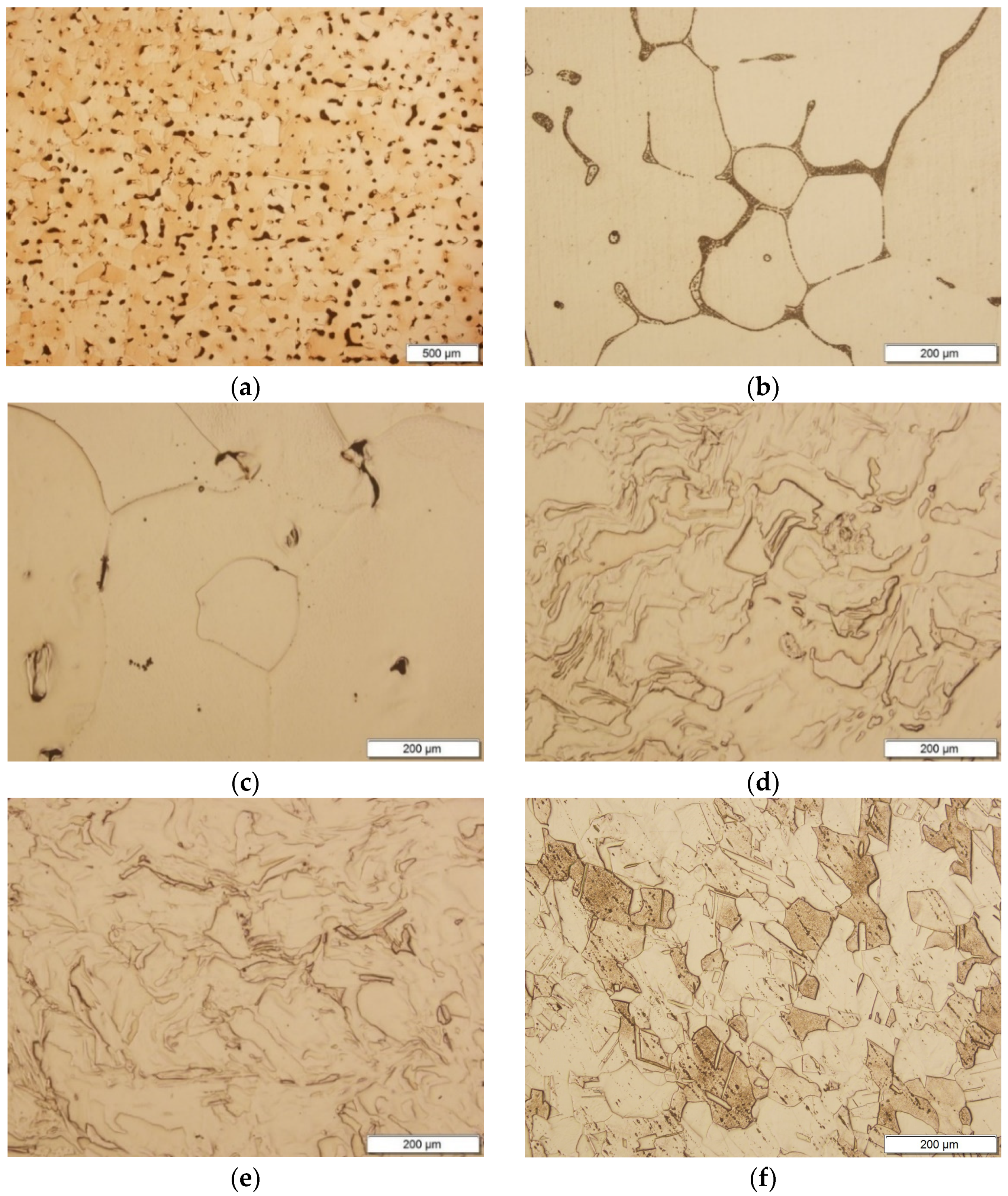
Figure 2 shows a representative surface appearance of components produced by all methods. The visual assessment of the outer surface of the contact elements already indicates the existence of significant differences in the surface development between the elements, resulting from the manufacturing technology used. Comparison of the surfaces shows best smoothness in the case of a conventionally manufactured element, for which the surface smoothness class depends on the machining method used and can be selected depending on a wide range of requirements. However, it should be noted that additional machining can also be applied to all other elements for the final surface treatment. When comparing the surface of raw products, it is necessary to emphasize the very good quality of the element after printing with the BJ method, with a characteristic fine texture ensuring relatively good smoothness. In this respect, printing with the DMLS method provides slightly worse results; however, this slightly higher roughness of the surface with a characteristic texture (similar to the surface after shot blasting), may be fully sufficient for most applications, and parts of the surface that require a better finish can be machined. The elements cast into sand moulds undoubtedly have the worst surface quality, which is a characteristic feature of this method.

3.2. Microstructure

The results of microscopic observations of the microstructure of samples obtained by all methods are shown in Figure 3.
The microstructure of BJ samples fully complies with the binder jetting technology and is typical for this type of material with the microporosity present in the entire volume of the material, with only local variation (see Figure 3a). Numerous micropores, in the order of several tens of micrometres, have complex shapes. The microstructure is characteristic of a fully recrystallized material with polygonal equiaxed grains. The microporosity of the material limits the grain size and inhibits grain growth.
In the case of the SC contact samples, a coarse-grained nature of the macrostructure is visible, typical for the cast and relatively slowly cooled material. There is a clear difference between the microstructure observed in the area at the outer contact surface (Figure 3b) and the microstructure in the middle section (see Figure 3c). The main difference is the presence of a casting structure with numerous regions of the Cu-Cu2O eutectic present at a depth of about 100 μm to even 500 μm, depending on the area of observation. It can be assumed that the surface oxidation of the liquid copper took place during the casting process, after the copper was poured into the mould. In the central areas of the sample, no oxide clusters are observed and the oxygen level is relatively low; however, a scattered microporosity is visible, mainly at the grain boundaries.
The microstructure of the DMLS contact is very fine-grained (see Figure 3d,e), uniform and very similar for both observed metallographic sections. There are no significant internal defects in the material, except for a few minor sub-surface areas of delamination and accidentally introduced impurities. The fine-grained nature of the microstructure and its morphology resemble hot-deformed but non-recrystallized material.
In the case of the sample from the SM contact, the microstructure (see Figure 3f) is typical for extruded copper of the Cu-ETP grade, additively drawn with a small degree of deformation, without visible internal defects, and with numerous visible twins. This results from the feedstock material used and is typical for extruded copper of the Cu-ETP grade, additionally drawn with a small degree of deformation.

3.3. Specific Density

The values of specific density obtained for the investigated components are presented in Table 2.
For components produced by additive manufacturing, it is important to evaluate the absence of defects in terms of the homogeneity of the material. In this respect, a good estimate is the specific density (see Table 2), the value of which is the highest for the element made in a conventional way by subtractive manufacturing (the SM element), which is typical for this technology. However, it should be emphasized that the DMLS element is characterized by only a slightly lower density value (0.3% lower than the density of the SM element). In this respect, the obtained value is definitely better than many results reported for samples made in a similar technology such as Selective Laser Melting (SLM) in [23,24], approaching the density assumed as characteristic for commercial annealed copper (8.89 g/cm3). A slightly lower value of the specific density was recorded for the cast sample (SC), which is related to the scattered microporosity and is typical for castings (Figure 3c). A much higher porosity related to the printing method used was noted for the sample made in the BJ technology (average porosity approx. 14 wt.%); however, this is a much better result compared to the porosities presented in [25] (from 77.8 ÷ 90.5% depending on the conditions). It should be emphasized that the density of prints in the BJ technology, if necessary, can be significantly improved using hot isostatic pressing (HIP) [26], which is also associated with a significant improvement in many other properties.
The visual assessment of the contact cross-sectional area, conducted for the subsurface layer after grinding of approximately 0.1 mm of the material, and the cross-section made in half the thickness of the elements, did not show (on a macro scale) the presence of internal defects. The homogeneity of the material should be assessed as good, and the components as practically defect-free.

3.4. Oxygen Content

For the tested elements, no classical chemical analysis was carried out to determine the chemical composition, with the exception of the analysis of the oxygen content, which resulted from the real possibility of introducing this element during the production process and its potential impact on functional properties. The results of these measurements (see Table 2) show highly variable levels of oxygen content when comparing different manufacturing methods. The oxygen content is the highest for the SM contact, which is associated with the use of a copper flat bar of the Cu-ETP grade for the production; the oxygen content found here is typical and falls within the standard range (the content of oxygen up to 400 ppm).
A similarly high level of oxygen content was also noted for the contact made using the DMLS printing technology. In this case, the oxygen content may be related to its presence in the powder itself (also due to surface oxidation), as well as to the oxidation introduced during the production process. For example, the high purity copper powder used in work [24] for SLM printing contained 423 ppm of oxygen, although unfortunately, the final content was not specified. It should be emphasized that the increased oxygen content is fully acceptable and does not differ from the level found in existing copper products, with the exception of oxygen-free copper grades used in applications requiring resistance to hydrogen embrittlement, in which the oxygen content in the products eliminates the possibility of using such material. The other two components, obtained by sand casting and binder jetting, were characterized by a lower oxygen content; however this still does not protect against the occurrence of hydrogen embrittlement.
It is, however, worth mentioning that in the case of the SC contact, the sample was taken from the centre of the contact, and metallographic tests revealed oxidation of the subsurface layers of the material, leading to the formation of the Cu-Cu2O eutectic (Figure 3b) at a depth from 0.1 to 0.5 mm, depending on the observation area. It should be emphasized here that the presence of eutectics in the surface regions does not have to be of great importance for the application of the contact, due to the frequent use of surface treatment of cast details.

3.5. Mechanical Properties

The evaluation of the mechanical properties in the compression tests of samples cut from the contacts, due to small size of components, was limited only to the determination of the value of the compressive yield strength Rcp0.2. The determined values (see Table 2) are comparable to the values obtained in the tensile test; hence, the evaluation can relate these values to the provided literature data.
The lowest value of Rcp0.2 was obtained for the sample from the BJ contact (Rcp0.2 = 71 MPa), which is fully understandable considering that the actual cross-section of the sample (including microporosity) was definitely smaller than the one used in the calculations. A slightly higher value of the Rcp0.2 yield strength was noted for the SC sample (Rcp0.2 = 81.1 MPa), which is also fully understandable and is a typical level for pure Cu of soft temper. For the sample from the SM contact, the value of Rcp0.2 indicates significant hardening of the material (258 MPa), which is characteristic of copper of the Cu-ETP grade in the hardened temper H075 (R280). The similar material in the DMLS contact showed a much lower value of Rcp0.2 (169 MPa), indicating the presence of strain hardening in the material. The value of Rcp0.2 is clearly higher than for copper in the annealed state and can be comparable with the H065/R230 temper. The results reported in the literature for components printed with similar methods are comparable. In the work [27], parts made of Cu printed with the EBM method had a yield point of 78 ÷ 88 MPa, while a significant anisotropy of properties was noted, as in the work for components printed with the SLM technology (yield point 125–157 MPa), or in the work [20], where the prints made with the SLM method showed even higher values of the yield point (186 MPa).
These results are consistent and follow the trend recorded for the hardness values of individual contacts as shown in Table 2 (see Figure S1 for a graphical representation of the results). In the case of BJ contact, the material is pure copper, but the obtained result is determined by a relatively high ratio of microporosity, which resulted in unnaturally low hardness values (in the range of 27 HV). In the case of the SC contact, the hardness of copper (45 HV) is relatively low, at the level typical for this state of the material. In this case, there were differences in hardness between the surface area (51.2 HV1) and the central area (41.3 HV1), which have their source in the presence of the Cu-Cu2O eutectic in the subsurface zone. The contact made using the DMLS method is characterized by increased hardness (approx. 80 HV1) compared to annealed copper, which proves that the material strengthened. This result is consistent with that reported in [24] for the SLM technology, where a hardness of 83.6 HV0.05 was demonstrated. This clearly indicates the residual hardening of the material after printing with the SLM method, which is clearly visible when comparing the hardness of the elements after, for example, printing with the EBM technology (30 ÷ 47 HV5 depending on the printing conditions [27]). On the other hand, the hardness level of 96 HV for copper in the SM contact is characteristic of a strain-hardened product (Cu-ETP copper, H085/H075 hardening temper). Slightly higher hardness values for the subsurface zone should be explained by additional hardening due to machining.

3.6. Electrical Conductivity

Some differentiation is also shown by the results of measurements of the electrical conductivity of the contacts, made on the same planes as the hardness measurements. The SM contact is characterized by the highest value of conductivity (above 100% IACS, as shown in Table 2; see also Figure S1 for a graphical representation of the results), which is fully understandable, since this is a typical value for pure copper of the Cu-ETP grade in the case of making an electrical contact out of it. Additionally, the very good homogeneity of the results should be underlined. A similarly high electrical conductivity was measured for the DMLS contact (98.5% IACS on average), also with very good homogeneity, which indicates good copper purity (no impurities introduced in the contact manufacturing process). The obtained results are much higher than the conductivity of 23.9 MS/m reported in [24], but on the other hand they are very consistent with the similarly high conductivity values obtained for the printed copper using the EBM method [27] where, depending on the process parameters, the components were characterized by conductivity from 55 to even 59 MS/m.
In the case of an SC contact, also made of pure copper, the conductivity also exceeds 100% IACS, but only in the subsurface layers, while in the centre of the element it drops to about 97% IACS. The variability of results is most likely related to the presence of large amounts of Cu-Cu2O eutectic, apparently increasing the electrical conductivity of copper. A high level of conductivity depends on the elimination of impurities, which is not always possible to achieve, even with a high-purity copper feedstock and thus a good purity of the casting. In such cases, the oxygen content in the metal changes the form of the impurity elements into oxide and improves the conductivity.
The BJ contact, also made of pure copper, due to its very high microporosity, is characterized by a significantly reduced conductivity, in the order of only 46 ÷ 48% IACS, which is completely inadequate for products made of Cu. In this case, the heterogeneity of the results is also visible, related to the variability of the microporosity ratio depending on the measurement place.

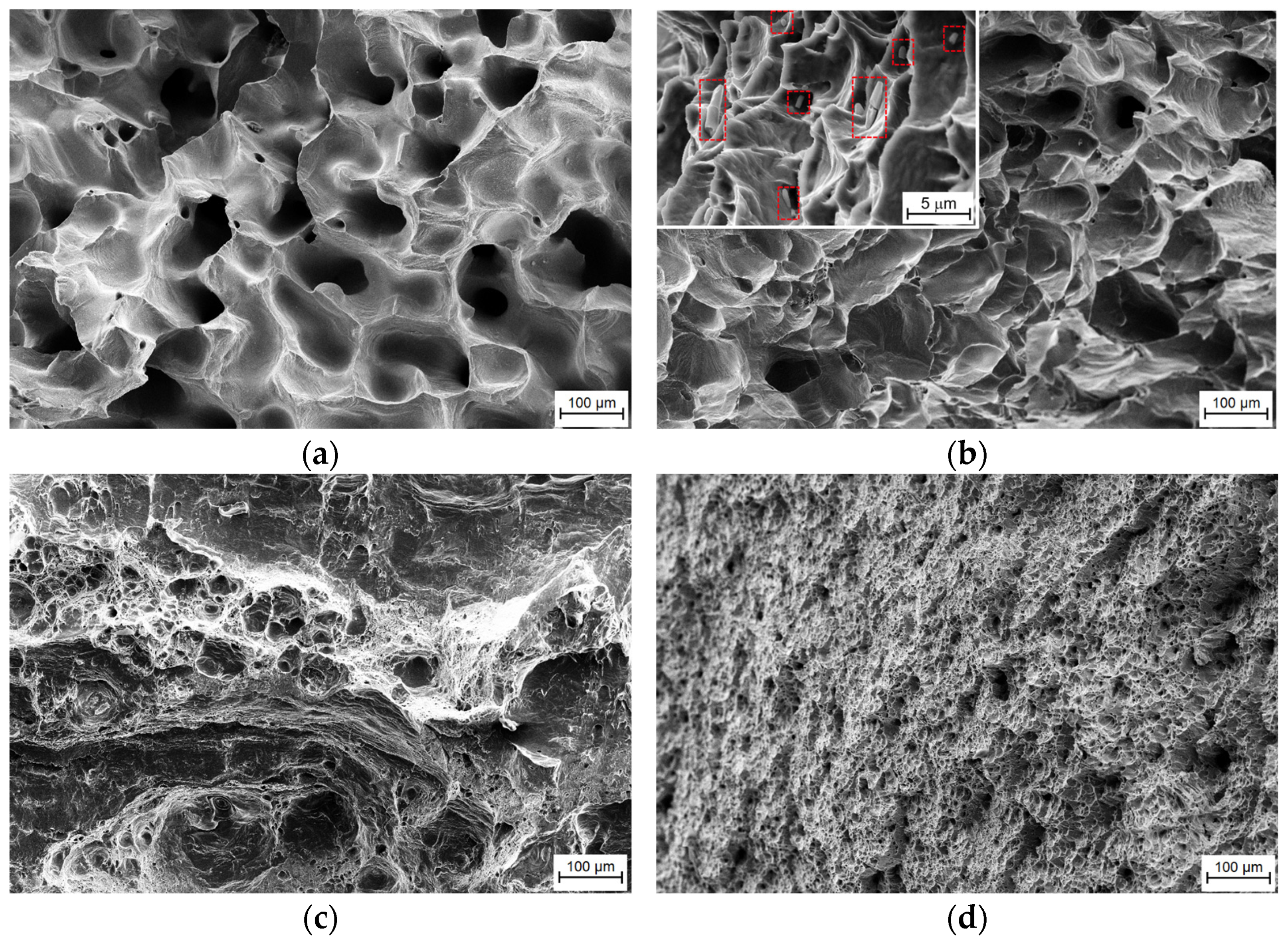
3.7. Fracture Characteristics

The results of the fractographic observations of the fractures are shown in Figure 4. The topography of the fractures varies depending on the production technology adopted, but in all cases the material showed a transcrystalline ductile fracture.
It should be noted that the fractures formed by bending the contact section (after it has been cut) have a morphology largely related to the mechanics of their formation. Transcrystalline ductile fracture (Figure 4d), which is homogeneous over the entire surface, with a system of small cavities with numerous Cu2O oxide particles (not visible in the shown photo at low magnification), is typical for most copper products, and the morphology is typical for Cu-ETP copper. It should be noted, however, that the nature of the fracture of the DMLS contact is significantly different, but also indicates a very high ductility of the material. The surface still shows typical indentations and traces of plastic flow of the material (Figure 4c), and in some areas of the fracture with a cleavage character. In this respect, these results are consistent with the fracture morphology for the samples studied in [24]. In the case of the SC sample, the coarse-grained microstructure of the casting results in a slightly different shape of the fracture topography, with clear traces of flow on the walls of the indentations (Figure 4b). At higher magnifications (see inset in Figure 4b), the eutectic regions with numerous oxide particles in the edge areas are clearly visible, while no oxides are observed in the middle part of the sample (Figure 4b). The BJ contact made with a different technology is characterized by a completely different morphology, associated with a large number of micropores, which are the cracks nuclei (Figure 4a). Metallic walls are characterized by high ductility subject to strong elongation, with traces of deformation lines on their surfaces. The fracture morphology has a “spongy” character, associated with the microstructure of the material, and the micropores are visible on the sample surface after the fracture, even at a relatively low magnification.

4. Conclusions

Thanks to the performed comprehensive analysis of the properties of 3D-printed copper parts and their comparison with classic manufacturing methods, the following conclusions can be drawn:
  • From the point of view of applications in the power and electronics industries, it is extremely important to emphasize the very good results of electrical conductivity obtained for components made by means of DMLS technology (>98.5% IACS), which are slightly lower than the value obtained for the reference sample.
  • DMLS technology led to a very good homogeneity and no microstructural defects, which is related to the very high values of the relative density.
  • Particularly noteworthy is the observed hardening present in the DMLS component after printing (at the level of material in the H80 state of hardening); therefore, DMLS technology provides properties that exceed the properties of components produced by sand casting.
  • In the case of BJ printed, it was possible to obtain a part with a low oxygen content; however, the mechanical and electrical properties were not sufficient.
  • The presented results are especially crucial for selection of the 3D-copper-printing method in the area of electrification, where rated operational voltages and currents are extremely high, and the manufactured electrical contact elements should ensure long-lasting and durable functionality in order to avoid the malfunctioning of switching and protection devices.

Supplementary Materials

The following supporting information can be downloaded at: https://www.mdpi.com/article/10.3390/met14090975/s1, Figure S1: Graphical representation of hardness and electrical conductivity results shown in Table 2. Data obtained for subsurface and middle area are separately presented.

Author Contributions

Conceptualization, W.M. and A.R.; methodology, J.K., R.S., W.M. and G.K.; validation, A.B. and A.R.; formal analysis, W.M., J.K., A.B., A.H., B.A., G.K. and R.R.; investigation, W.M., A.B., G.K. and R.S.; resources, A.H., R.R., B.A., W.M. and A.B.; data curation, A.B., J.K., W.M., G.K. and R.S.; writing—original draft preparation, W.M. and A.R.; writing—review and editing, J.K. and A.B.; visualization, W.M. and G.K. All authors have read and agreed to the published version of the manuscript.

Funding

This research received no external funding.

Data Availability Statement

The original contributions presented in the study are included in the article/supplementary material, further inquiries can be directed to the corresponding author.

Conflicts of Interest

Authors Bartlomiej Adamczyk, Ryszard Rzepecki and Andrzej Rybak were employed by the company ABB Corporate Technology Center. The remaining authors declare that the research was conducted in the absence of any commercial or financial relationships that could be construed as a potential conflict of interest.

References

  1. Jiang, Q.; Zhang, P.; Yu, Z.; Shi, H.; Wu, D.; Yan, H.; Ye, X.; Lu, Q.; Tian, Y. A Review on Additive Manufacturing of Pure Copper. Coatings 2021, 11, 740. [Google Scholar] [CrossRef]
  2. Sun, C.; Wang, Y.; McMurtrey, M.D.; Jerred, N.D.; Liou, F.; Li, J. Additive manufacturing for energy: A review. Appl. Energy 2021, 282, 116041. [Google Scholar] [CrossRef]
  3. Stavropoulos, P.; Foteinopoulos, P.; Papacharalampopoulos, A.; Bikas, H. Addressing the challenges for the industrial application of additive manufacturing: Towards a hybrid solution. Int. J. Lightweight Mater. Manuf. 2018, 1, 157–168. [Google Scholar] [CrossRef]
  4. Zhou, L.; Miller, J.; Vezza, J.; Mayster, M.; Raffay, M.; Justice, Q.; Al Tamimi, Z.; Hansotte, G.; Sunkara, L.D.; Bernat, J. Additive Manufacturing: A Comprehensive Review. Sensors 2024, 24, 2668. [Google Scholar] [CrossRef] [PubMed]
  5. Selema, A.; Ibrahim, M.N.; Sergeant, P. Metal Additive Manufacturing for Electrical Machines: Technology Review and Latest Advancements. Energies 2022, 15, 1076. [Google Scholar] [CrossRef]
  6. Mooraj, S.; Qi, Z.; Zhu, C. 3D printing of metal-based materials for renewable energy applications. Nano Res. 2021, 14, 2105–2132. [Google Scholar] [CrossRef]
  7. Yan, X.; Chang, C.; Dong, D.; Gao, S.; Ma, W.; Liu, M.; Liao, H.; Yin, S. Microstructure and mechanical properties of pure copper manufactured by selective laser melting. Mater. Sci. Eng. A 2020, 789, 139615. [Google Scholar] [CrossRef]
  8. Ladani, L.; Sadeghilaridjani, M. Review of Powder Bed Fusion Additive Manufacturing for Metals. Metals 2021, 11, 1391. [Google Scholar] [CrossRef]
  9. Vafadar, A.; Guzzomi, F.; Rassau, A.; Hayward, K. Advances in Metal Additive Manufacturing: A Review of Common Processes, Industrial Applications, and Current Challenges. Appl. Sci. 2021, 11, 1213. [Google Scholar] [CrossRef]
  10. Ngoa, T.D.; Kashania, A.; Imbalzanoa, G.; Nguyena, K.T.Q.; Hui, D. Additive manufacturing (3D printing): A review of materials, methods, applications and challenges. Compos. Part B Eng. 2018, 143, 172–196. [Google Scholar] [CrossRef]
  11. Gokuldoss, P.K.; Kolla, S.; Eckert, J. Additive Manufacturing Processes: Selective Laser Melting, Electron Beam Melting and Binder Jetting—Selection Guidelines. Materials 2017, 10, 672. [Google Scholar] [CrossRef] [PubMed]
  12. Ahmadi, M.; Bozorgnia Tabary, S.A.A.; Rahmatabadi, D.; Ebrahimi, M.S.; Abrinia, K.; Hashemi, R. Review of selective laser melting of magnesium alloys: Advantages, microstructure and mechanical characterizations, defects, challenges, and applications. J. Mater. Res. Technol. 2022, 19, 1537–1562. [Google Scholar] [CrossRef]
  13. Azami, M.; Siahsarani, A.; Hadian, A.; Kazemi, Z.; Rahmatabadi, D.; Kashani-Bozorg, S.F.; Abrinia, K. Laser powder bed fusion of Alumina/Fe–Ni ceramic matrix particulate composites impregnated with a polymeric resin. J. Mater. Res. Technol. 2023, 24, 3133–3144. [Google Scholar] [CrossRef]
  14. Mohsan, A.U.H.; Wei, D. Advancements in Additive Manufacturing of Tantalum via the Laser Powder Bed Fusion (PBF-LB/M): A Comprehensive Review. Materials 2023, 16, 6419. [Google Scholar] [CrossRef] [PubMed]
  15. Zhang, Y.; Li, Y.; Song, M.; Li, Y.; Gong, S.; Zhang, B. TiAl Alloy Fabricated Using Election Beam Selective Melting: Process, Microstructure, and Tensile Performance. Metals 2024, 14, 482. [Google Scholar] [CrossRef]
  16. ISO/ASTM 52900:2021-11; Additive Manufacturing—General Principles—Fundamentals and Vocabulary. ISO: Geneva, Switzerland, 2021.
  17. Tran, T.Q.; Chinnappan, A.; Kong Yoong Lee, J.; Huu Loc, N.; Tran, L.T.; Wang, G.; Kumar, W.V.; Jayathilaka, V.A.; Ji, D.; Doddamani, M.; et al. 3D Printing of Highly Pure Copper. Metals 2019, 9, 756. [Google Scholar] [CrossRef]
  18. Singer, F.; Deisenroth, D.C.; Hymas, D.M.; Dessiatoun, S.V.; Ohadi, M.M. Additively Manufactured Copper Components and Composite Structures for Thermal Management Applications. In Proceedings of the 16th IEEE Intersociety Conference on Thermal and Thermomechanical Phenomena in Electronic Systems (ITherm), Orlando, FL, USA, 30 May–2 June 2017. [Google Scholar] [CrossRef]
  19. El-Wardany, T.I.; She, Y.; Jagdale, V.N.; Garofano, J.K.; Liou, J.J.; Schmidt, W.R. Challenges in Three-Dimensional Printing of High-Conductivity Copper. Mater. Sci. J. Electron. Packag. 2018, 140, 020907. [Google Scholar] [CrossRef]
  20. Ziaee, M.; Crane, N.B. Binder jetting: A review of process, materials, and methods. Addit. Manuf. 2019, 28, 781–801. [Google Scholar] [CrossRef]
  21. Gong, G.; Ye, J.; Chi, Y.; Zhao, Z.; Wang, Z.; Xia, G.; Du, X.; Tian, H.; Yu, H.; Chen, C. Research status of laser additive manufacturing for metal: A review. J. Mater. Res. Technol. 2021, 15, 855–884. [Google Scholar] [CrossRef]
  22. Gerapid High Speed DC Breakers 2600–8000 A. Available online: https://library.industrialsolutions.abb.com/publibrary/checkout/170131_EN?TNR=Brochures%7C170131_EN%7CPDF&filename=170131_EN.pdf (accessed on 5 August 2024).
  23. Sinico, M.; Cogo, G.; Benettoni, M.; Calliari, M.; Pepato, A. Influence of Powder Particle Size Distribution on The Printability of Pure Copper For Selective Laser Melting, Solid Freeform Fabrication 2019. In Proceedings of the 30th Annual International Solid Freeform Fabrication Symposium—An Additive Manufacturing Conference Reviewed Paper, Austin, TX, USA, 12–14 August 2019. [Google Scholar]
  24. Huang, J.; Yan, X.; Chang, C.; Xie, Y.; Ma, W.; Huang, R.; Zhao, R.; Li, S.; Liu, M.; Liao, H. Pure copper components fabricated by cold spray (CS) and selective laser melting (SLM) technology. Surf. Coat. Technol. 2020, 395, 125936. [Google Scholar] [CrossRef]
  25. Kumar, A.Y.; Bai, Y.; Eklund, A.; Williams, C.B. The effects of Hot Isostatic Pressing on parts fabricated by binder jetting additive manufacturing. Addit. Manuf. 2018, 24, 115–124. [Google Scholar]
  26. Kumar, A.Y.; Wang, J.; Bai, Y.; Huxtable, S.T.; Williams, C.B. Impacts of process-induced porosity on material properties of copper made by binder jetting additive manufacturing. Mater. Des. 2019, 182, 108001. [Google Scholar] [CrossRef]
  27. Guschlbauer, R.; Momeni, S.; Osmanlic, F.; Körner, C. Process development of 99.95% pure copper processed via selective electron beam melting and its mechanical and physical properties. Mater. Charact. 2018, 143, 163–170. [Google Scholar] [CrossRef]
Figure 1. Images of the arcing contacts which were manufactured and used for investigation: (a) reference sample made by SM, (b) 3D printed part by means of BJ process. (c) image of DC high-speed circuit breaker with indicated location of the investigated arcing contact. Reprinted from Ref. [22].
Metals 14 00975 g001
Figure 2. Characteristic appearance of the surface texture of copper elements made with various technologies: (a) BJ; (b) SC; (c) DMLS; (d) SM.
Metals 14 00975 g002
Figure 3. Microstructure of the samples manufactured by various methods, etched samples. (a) BJ (b) SC—subsurface plane (c) SC—middle plane (d) DMLS—subsurface plane (e) DMLS—middle plane (f) SM.
Metals 14 00975 g003
Figure 4. Topography of the fracture surfaces of the samples obtained by all methods: (a) BJ; (b) SC (inset shows higher magnification with the oxide particles marked by red frames); (c) DMLS; (d) SM.
Metals 14 00975 g004
Table 1. Component designation and materials used and their manufacturing technology.
Sample NameManufacturing TechnologyMaterials UsedManufacturing Conditions
BJBinder JettingCopper powder: Cu > 99.95%, C = 0.03%, Fe = 0.01%; d50 = 44 μmMetal printing with ExOne X1 25Pro (ExOne, North Huntingdon, PA, USA) printer: layer thickness: 50 µm, organic additive: water-based polymer binder (curing temp. 180 °C), sintering temp.: 840–900 °C
SCSand CastingOxygen-free copper (O2 < 0.001%) in form of wireSand mould printed with ExOne S-Max (ExOne, North Huntingdon, PA, USA) printer: FS001 quartz sand with size: 0.13–0.14 mm, layer thickness: 0.28 mm, furan binder. Copper casting temp.: 1085 °C
DMLSDirect Metal Laser SinteringCuCP powder: Cu > 99.95%, O2 = 0.04%, d50 = 40 μm, particle distribution: 15–53 μmMetal printing with EOS M 290 (EOS GmbH, Krailling, Germany): Yb-fiber laser, 1 × 400 W, focus diameter: 100 µm, scanning rate: 7.0 m/s, build platform heating:450 °C, post-heating: 1000 °C/1 h under argon
SMSubtractive ManufacturingCu-ETP in H075/R280 temper: Cu > 99.9%, Bi < 0.0005%, O2 < 0.04%, Pb < 0.005%Machining from a flat copper bar with use of computer numerical control (CNC) milling machine: 2-flute tungsten carbide cutter, diameter: 2 mm, speed: 365 m/min, feed rate: 0.02 mm/rev
Table 2. Material properties of components manufactured by various methods.
Material PropertiesManufacturing Method
BJSCDMLSSM
Specific density, g/cm37.588.728.838.86
Oxygen content, ppm6289 (1)253261
Yield strength, Rcp0.2, MPa71.085.1169258
HV1Measurement areasubsurfacemiddlesubsurfacemiddlesubsurfacemiddlesubsurfacemiddle
Average26.927.851.241.381.878.299.492.8
Std. deviation1.81.65.34.57.73.72.62.5
ConductivityAverageMS/m26.8228.0558.0556.4557.1657.1258.5358.56
Std. dev.0.440.370.140.080.060.190.060.08
Average value%IACS46.248.4100.197.398.698.5100.9101.0
(1) the given value of oxygen content refers to a sample taken from the centre of the element, disregarding the surface zone.
Disclaimer/Publisher’s Note: The statements, opinions and data contained in all publications are solely those of the individual author(s) and contributor(s) and not of MDPI and/or the editor(s). MDPI and/or the editor(s) disclaim responsibility for any injury to people or property resulting from any ideas, methods, instructions or products referred to in the content.

