Article

Impurity Behavior in Cast Copper Anodes: Implications for Electrorefining in a Circular Economy

by
Agustin Morales-Aragon
1,2,3,
Daniel Sánchez-Rodas
2,3,
Guillermo Ríos
1 and
Michael S. Moats
4,5,*
1
Atlantic Copper SLU, Avenida Francisco Montenegro, 21001 Huelva, Spain
2
Center for Research in Sustainable Chemistry-CIQSO, University of Huelva, 21007 Huelva, Spain
3
Department of Chemistry, University of Huelva, 21007 Huelva, Spain
4
O’Keefe Center for Critical Minerals, Missouri University of Science and Technology, Rolla, MO 65409, USA
5
Department of Materials Science and Engineering, Missouri University of Science and Technology, Rolla, MO 65409, USA
*
Author to whom correspondence should be addressed.
Metals 2025, 15(2), 113; https://doi.org/10.3390/met15020113
Submission received: 4 December 2024 / Revised: 13 January 2025 / Accepted: 17 January 2025 / Published: 24 January 2025
(This article belongs to the Section Metal Casting, Forming and Heat Treatment)

Abstract

:
The behavior of impurities in cast copper was investigated to simulate production with increased utilization of secondary sources within the framework of a circular economy. The incorporation of impurities, particularly Ni, Sn, and Sb, from recycled Cu may significantly impact the electrorefining process. In this study, commercial anodes were doped with Ni, Sn, and Sb concentrations of 2500–6500 g/t, 300–900 g/t, and 450–950 g/t, respectively. Anode concentrations of Pb and Bi were maintained at 1000 g/t and 350 g/t, respectively. As concentrations were examined at two levels, 860 or 1700 g/t, depending on the commercial anode used to create the doped samples. Electron microscopy with microprobe analysis revealed that the commercial anodes contained three predominant phases: Cu2O, (Cu,Ag)2(Se,Te), and a complex oxide phase of Cu, Pb, As, Sb, and/or Bi. Ni, the main impurity, primarily accumulated within the Cu grains, while Sn and Sb tended to form oxidized inclusions. The distribution of Ni in Cu grains was ca. 20% lower in the anodes doped at higher Ni concentrations due to the formation of nickel-bearing inclusions, such as Kupferglimmer and NiO. The doped anodes showed lower quantities of Cu2O inclusions than the commercial anodes due to the preferential formation of oxides with other impurities, including SnO2. These findings highlight potential challenges for Cu electrorefining in a circular economy, as Ni, Sb, and Sn may impact the deportment of these impurities to slimes or electrolyte and may cause copper depletion in the refining electrolyte.

1. Introduction

Increasing human population, non-renewable resource utilization, and waste generation are changing our planet. To reverse societal impacts, a more circular economy is needed to replace the current production model based on “take–make–dispose”. In a circular economy, the aim is to maximize resource efficiency by extending product life cycles, promoting reuse, employing remanufacturing techniques, and utilizing wastes as resources [1,2,3].
With the ongoing green energy transition, the global demand for refined copper (Cu) increased by 2.7% in 2023, and it is expected to rise by 50% by 2040 [4]. This may result in supply limitations [5] as global Cu mine production is anticipated to peak due to decreasing ore grades [6,7]. Thus, increasing the recycling rate of Cu is foreseen as a global need [2].
Secondary supply and re-use are forecasted to account for more than 50% of the anticipated increase in copper demand [4]. In highly industrialized areas with an established recycling industry, such as Europe, secondary Cu (obtained from scrap) represents ca. 40% of the total demand, and it has been projected that it will reach 65% [7]. In other regions, like China, it is expected to account for 80% of the demand for recycled domestic scrap [8]. Since copper can be recycled without losing its chemical or physical properties, processing more secondary copper sources is very feasible [9].
The largest source of Cu scrap for future secondary smelters is anticipated to be waste electrical and electronic equipment (WEEE). The amount of WEEE collected in Europe is growing by 3–5% per year [10]. Currently, only about 10% WEEE is of suitable quality for copper smelters, resulting in losses of copper to landfills, but recycling is expected to increase as device designs change in accordance with the demands of a circular economy [11,12].
Most valuable components of WEEE are related to PCBs [13,14]. The composition of PCBs is variable, with the Cu content ranging from 6 to 40 %, while the grades of Fe, Al, Sn, Pb, Ni, Sb, Cr, Ag, Pd, Bi, and Co range from 1.2 to 8 %, 0.3 to 7.2%, 1 to 6.3 %, 1 to 4.2 %, 0 to 5.4%, 0.1 to 0.4 %, 0.04 to 0.13 %, 0.01 to 0.45 %, 0 to 0.4 %, 0.006 to 0.01 %, and 0 to 0.4 %, respectively [13]. However, from these impurities, only Sn, Ni, Sb, Bi, Ag, and Pd have been reported to be present in anodes to a significant extent during copper pyrometallurgical processes [15].
Secondary copper can be incorporated into existing primary processing methods. The addition of scrap as cold charge into a converting furnace is a common practice. However, scrap can also be fed into smelting or anode furnaces. Furnace scrap addition is an energy consumer, as latent heat is consumed to melt the solid material. This counteracts the heat generated by sulfur oxidation during smelting or converting, or by combustion during fire refining. Thus, the quantity of secondary copper that can be added to primary smelting furnaces is limited by the heat balance of the system [16]. Fortunately, scrap is needed during matte converting because of excess heat generated during iron removal and copper making. While secondary copper can be recycled into the anode furnace, it is more common to just add scrap anodes from the electrorefining process [17].
Since the ability to add copper scrap into primary furnaces is limited and a certain scrap quality is required, smelters designed to only treat secondary scrap are increasingly being built. Secondary copper smelters use top-submerged lance furnaces and top-blown rotary convertors to smelt scrap with low-Cu grades [18]. The smelting product contains 80 % Cu (molten black Cu), which is converted to rough Cu with 96% purity and then fire-refined and cast into anodes for electrorefining (98.5% Cu).
Most high-purity (>99.99%) refined Cu is produced by electrorefining [17]. The electrorefining process is impacted by the presence of impurities in the anodes. Previous characterizations of refinery anodes and impurity deportment during electrorefining have focused mainly on materials generated by primary processing of concentrates. The impact of increased scrap utilization (e.g., secondary copper) on anode microstructure, impurity deportment during casting, and electrorefining is less well established [19]. The incorporation of more WEEE into the Cu production process will generate extra inputs of certain impurities (e.g., Sb, Sn, Ni, and Pb) that may affect the ability to produce high-purity copper through electrorefining. These impurities can affect electrolyte conductivity, current efficiency, slime production, slime leachability, and anode passivation [20,21,22,23,24,25].
In this context, Atlantic Copper, a primary Cu smelter located in Southern Europe, is undertaking an innovative project in which a primary smelter is combined with a secondary smelter to produce anodes for a single electrorefining facility where high-purity copper will be produced. The combination of primary and secondary materials in a novel approach justifies the necessity of studying the behavior of the impurities coming from the WEEE and their impact on electrorefining. It is anticipated that increases in Ni, Sn, and Sb will occur and potentially be the most challenging impurities resulting from increased utilization of WEEE [26].
Prior to electrorefining, anodes with increased Ni, Sb and Sn contents will be cast with copper produced from a combination of primary and secondary sources. During anode solidification, elements can either be soluble in solid copper grains or increase in concentration in remaining molten phase. This tendency is described by their distribution coefficient, k. The distribution coefficient is a parameter that describes the deportment of an element to report to crystallized Cu or melting the solidification process. This coefficient is defined as:
k = C S C L
where C S is the concentration of the element in solid copper and C L is the element concentration in the melt or liquid. If k is greater than 1, this element occurs preferentially in solid solution and if k is less than 1, this element will accumulate in the molten phase until a separate phase forms [27]. Cooling rates can affect the effective k value observed in copper anodes as non-equilibrium conditions can occur due to the fast cooling rates employed industrially.
Impurities that accumulate in the molten phase tend to form oxides due to the presence of oxygen, which has a k value of ~0.01 [22]. Oxide phases are immiscible with solid and molten copper and result in impurity precipitation and accumulation along grain boundaries and at grain corners because these volumes are the last to freeze. Anoxide compounds with a Gibbs free energy of formation (ΔGf) which is more negative than the ΔGf of Cu2O are thermodynamically more stable than Cu2O, and then form insoluble particles. Oxide compounds with higher ΔGf than the ΔGf of Cu2O will not form, and the metallic or metalloid elements will be found in solid solutions. Some impurities are found in oxide inclusions and Cu grains due to the combination of their distribution coefficients, nonspontaneous formation of oxides due to low concentrations, and/or kinetic limitations.
During electrorefining, more than 95% of the anode impurities report to the electrolyte or slimes. Impurities in solid solution with Cu are in elemental form. They will dissolve into the electrolyte at the anode surface during the electrorefining process. Once in the electrolyte, these elements may (1) remain in solution and diffuse away from the anode surface into the bulk electrolyte or (2) precipitate due to solubility constraints and produce slime phases. Impurities that are part of inclusions may report directly to the slimes if the inclusions do not dissolve into the electrolyte or may dissolve if the inclusion is acid-soluble. Specifically, NiO, Kupferglimmer and SnO2 inclusions are refractory in nature and do not readily dissolve during electrorefining [20]. Complex oxides of Cu-Pb-As-Sb-Bi may or may not dissolve based on prior characterization [28]. Therefore, the analysis of impurity content in both Cu grains and inclusions found in copper anodes produced from primary and secondary sources is needed to understand the future deportment of elements, such as Ni, Sb, and Sn, during electrorefining.
To investigate the impact of potential increases in the Ni, Sn and Sb to copper anodes, primary anodes from Atlantic Copper (AC) were melted in a laboratory-scale furnace and doped with these impurities. The resulting “doped anodes” (DAs) were physically characterized to examine the deportment of impurities in the cast anode microstructures with heightened attention to the concentration of these elements in solid solution within the Cu grains and the oxide inclusions.

2. Materials and Methods

Doped Anodes with Ni, Sn and Sb

Two commercial anodes from the Atlantic Copper refinery in Huelva, Spain, named AC1 and AC2 (each ca. 300 kg), were selected and the concentrations of the major impurities were determined using optical emission spectrometry (OES) (Thermo Scientific ARL 4460 OES, Waltham, MA, USA) (Table 1), using ERM-EB074A (electrolytic copper) as reference material. Oxygen was determined using an elemental analyzer (Eltra ON900, Eltra GmbH, Hann, Germany) within a calibration range of 100–5000 g/t. The two anodes were selected based on their arsenic concentration (anode AC1—a lower As value; anode AC2—a higher As value). Two commercial anodes with different As concentrations were selected due to restrictions at the casting laboratory with adding As. Pb and Sn were 3-fold higher in concentration in AC1 as compared to AC2. Chemical composition of the doped anodes was selected based on the projected inputs of incoming WEEE feed to a top submerged lance (TSL) furnace that could be installed at Atlantic Copper.
Each commercial anode was sectioned into 30 kg pieces. The pieces were melted and doped with Ni, Sn, Sb or a combination thereof, and casted at the Institute for Process Metallurgy and Metal Recycling (IME RWTH, University of Aachen, Aachen, Germany), as shown in Figure S1 in the Supplementary Information. This institute has the facilities to cast experimental Cu anodes [29,30,31,32,33]. After casting, rectangular specimens (19 cm × 21.5 cm) were obtained and employed as anodes in subsequent laboratory-scale electrorefining experiments not reported here. Circular (2.5 cm diameter) and rectangular (0.5 cm × 1 cm) specimens were also obtained from each casting for OES and electron probe microanalysis (EPMA). The design of the different samples obtained from cast experimental anodes is shown in Figure S2.
EMPA was performed with a JEOL JXA-8200 Super Probe (JEOL Ltd., Tokyo, Japan) using an accelerating voltage of 20 kV and a current of 20 nA. Standards for each element were used for calibration of the equipment. Limits of detection were determined during calibration which employed a ZAF matrix effect correction. The detection limits of the elements analyzed by EPMA (in wt.%) were As 0.05; Ni 0.04; Sb 0.03; Sn 0.04. The calculation of the limits of detection (LD) was carried out using Equation (2):
L D   p p m = 1 I n e t   S T D m a s s   ( % ) S T D 2   x   I b a c k t b a c k
where Iback is the average intensity of background X-ray signals, tback is the counting time of the background X-ray signals, InetSTD is the intensity of net X-rays of the standard sample, and mass (%)STD is the mass concentration in weight percent of the standard sample.
A total of 13 doped laboratory anodes were manufactured from samples of AC1 and AC2. For each DA, elements were added to achieve either a low or a high concentration of Ni, Sn, and/or Sb. Impurity concentrations as measured by OES for the doped anodes are summarized in Table 1. Impurities ranges were ca. 2500–6500 g/t for Ni, 300–900 g/t for Sn and 450–950 g/t for Sb. Other elements, such as Pb and Bi, were also doped to maintain their concentrations at ca. 1000 g/t and ca. 350 g/t, respectively.
The 0.5 cm × 1 cm specimens were polished (Figure S3) following the methodology described in Table S1 and analyzed by optical microscopy and EPMA. Optical microscopy was employed to analyze the Cu grains sizes of AC1, AC2 and the doped anodes. Two specimens were considered for each anode for grain size analysis. EPMA provided compositional data for Cu grains and inclusions. Field emission scanning electron microscopy (FESEM, model JEOL IT-300HR-LV, JEOL Ltd., Tokyo, Japan) with an acceleration voltage of 20 kV, a probe current of 70% and a working distance of 10 mm was employed to appreciate the structure of the inclusions smaller than 5 μm in size that formed around Cu grains. The FESEM had higher limits of detection (0.1–0.5 %wt range) than the EPMA employed in this study.

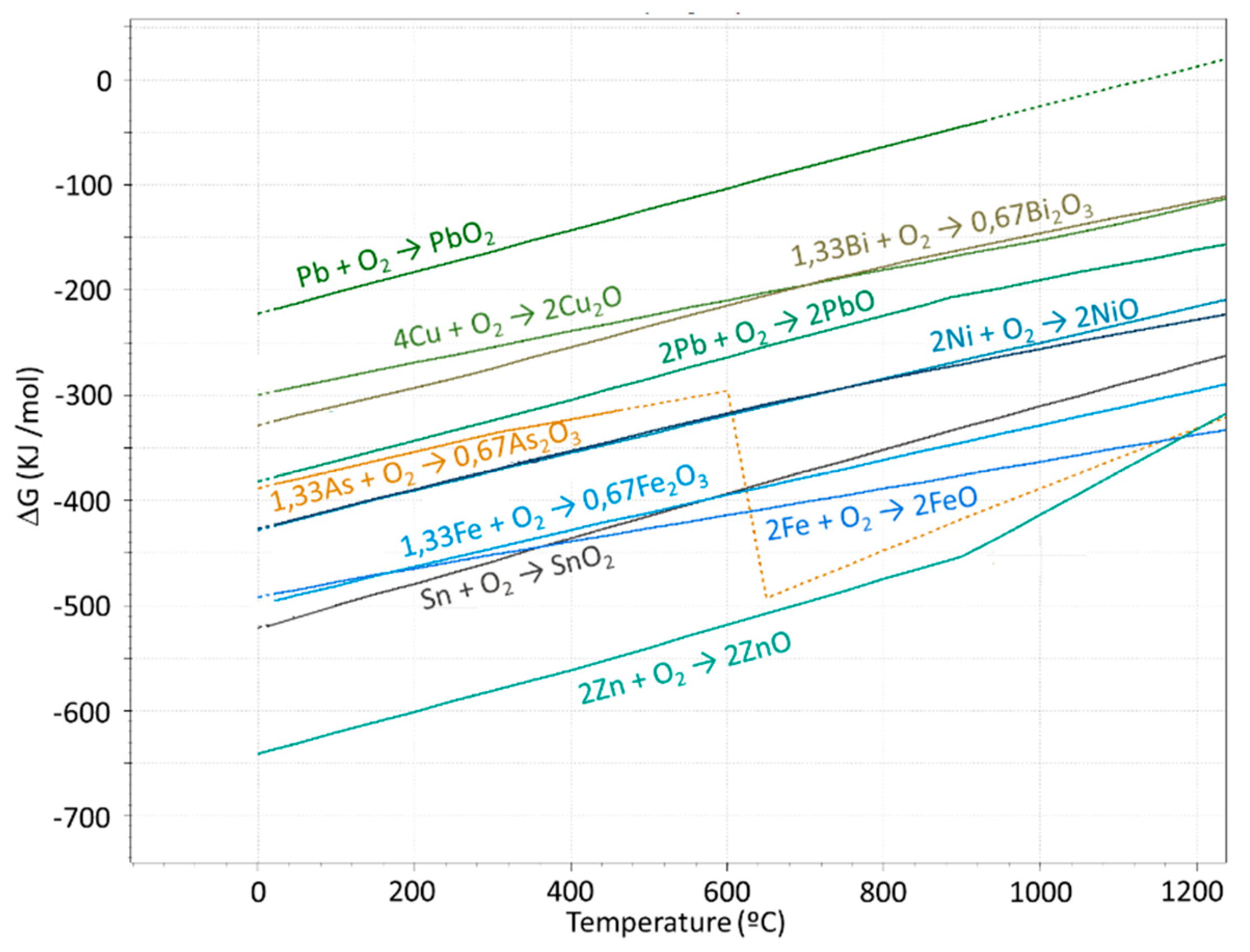
3. Results and Discussion

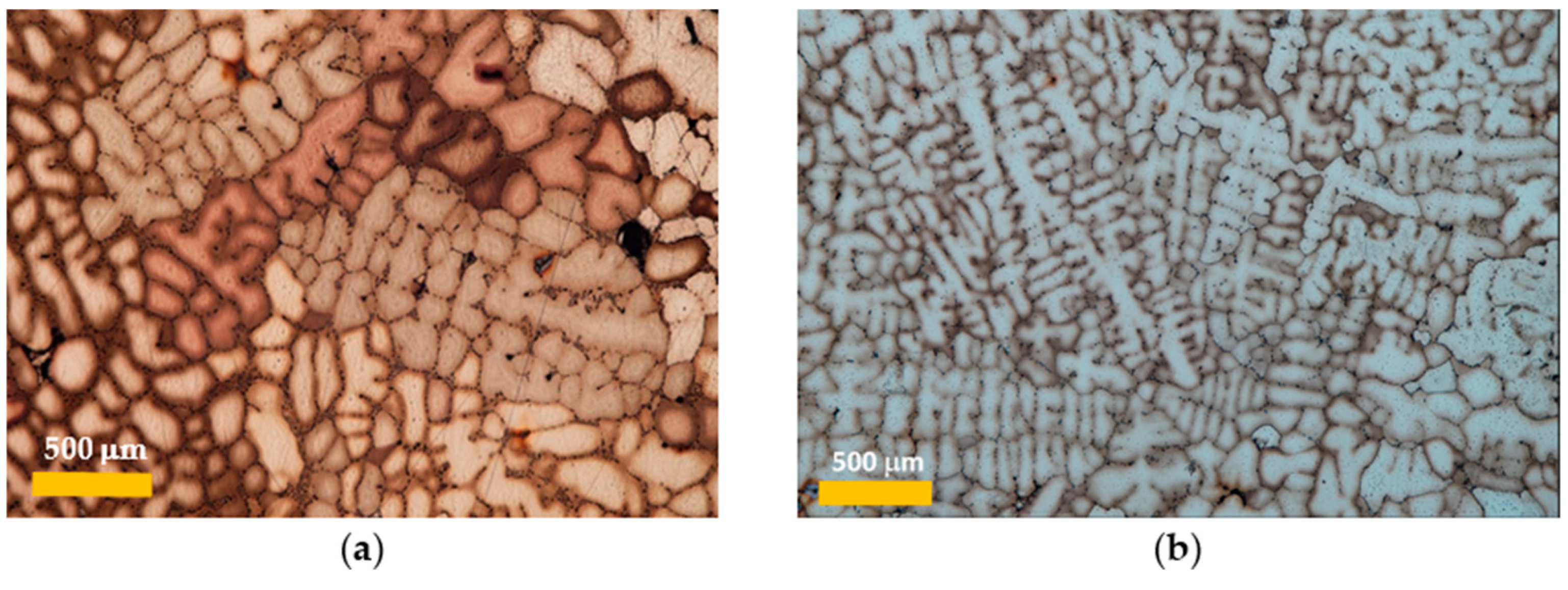
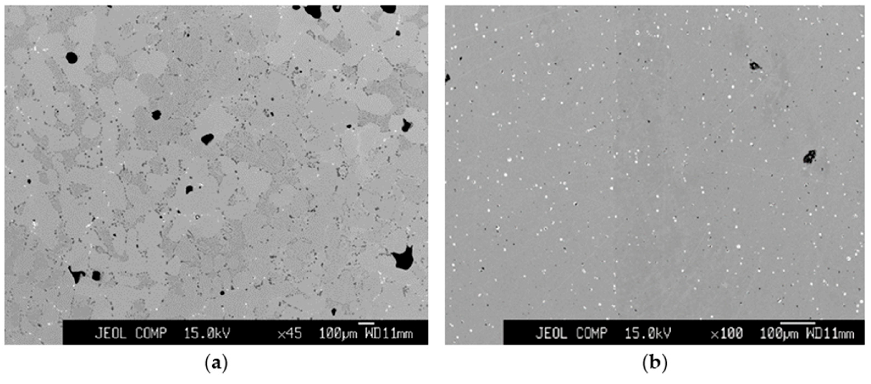
3.1. Grain Size Distribution

The intention of this work was to simulate the production of anodes containing copper produced from a combination of primary and secondary sources. Anode production at Atlantic Copper utilizes a casting wheel where the cooling rate is controlled by water cooling of copper molds. Casting parameters such as superheat temperature and heat removal rate result in microstructures with a range of grain sizes. Thus, it is important when casting anode materials in a laboratory that simulates future production to have similar grain sizes and microstructures.
Using optical microscopy, copper grain sizes of commercial anodes and doped anodes were examined (Figure 1). A total of 500 Cu grains per anode were analyzed using NIS_Elements software v. 5.21.00 to determine the average grain size [34]. It was found that Cu grain sizes in the commercial anodes ranged from 100 to 150 μm, and grain sizes in doped anodes ranged from 90 to 130 μm. While Mitan [34] correlated decreasing grain size with increasing impurity concentrations in industrial copper anode samples, no correlation was found in this study.
Grain size can be impacted by casting parameters, metal composition and the presence of secondary phases. To ensure that the casting process in the laboratory replicated the industrial process, an experiment was conducted where doping impurities were not added to commercial anode samples. The grain size distribution in the resulting laboratory anode was comparable to the commercially cast anodes. This indicated the laboratory casting procedure produced microstructures like the industrial process. Thus, the doped impurities examined in this study did not significantly impact grain size in the cast anodes at the levels studied [27].
The Cu grains, as shown in Figure 1, were dendritic. The texture of the Cu grains near the anode surface tended to be irregular because of rapid solidification caused by water cooling the mold. Cu grains were coarser away from the surface due to a slower cooling rate. This pattern is common in anodes casted on an industrial casting wheel. Copper grains are also larger toward the open face of the casting due to the slower cooling rate at the copper–air interface [20].

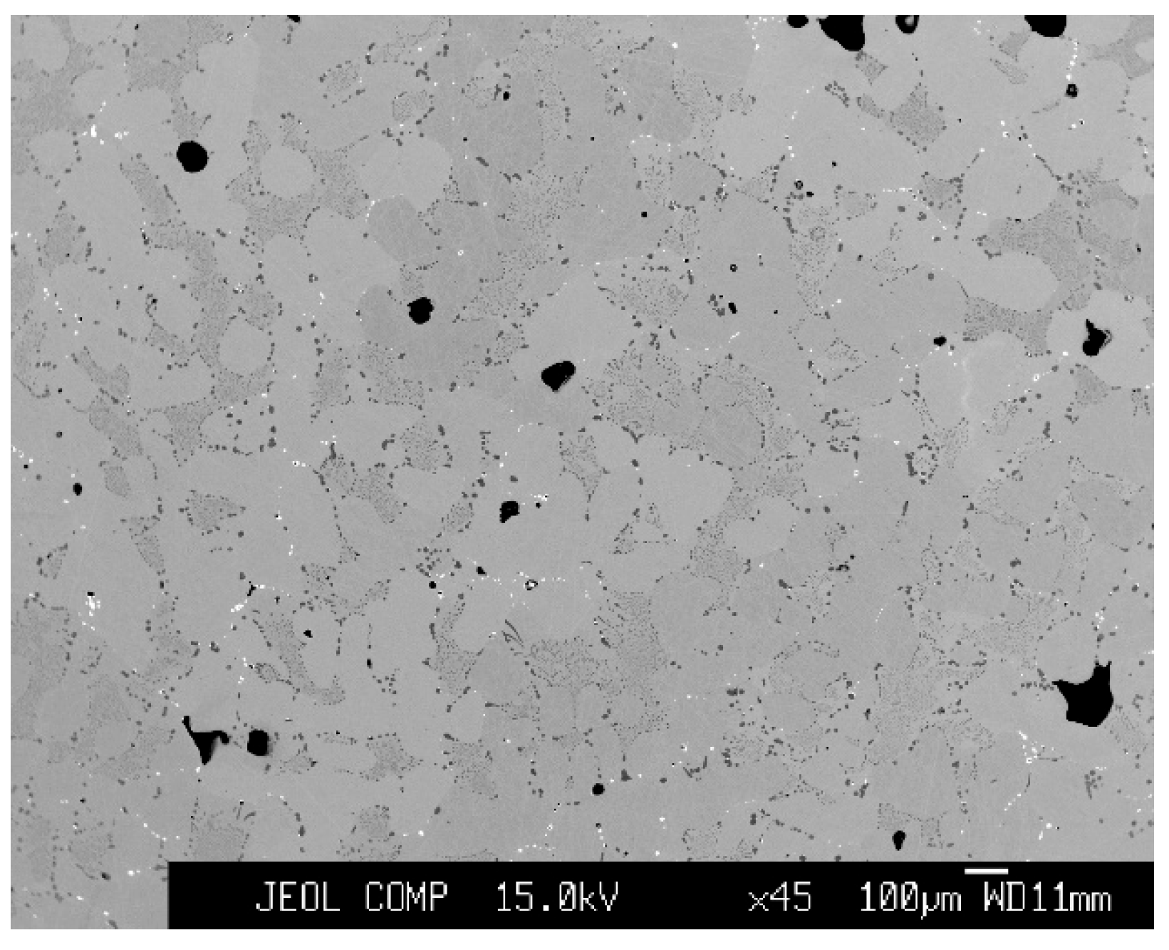
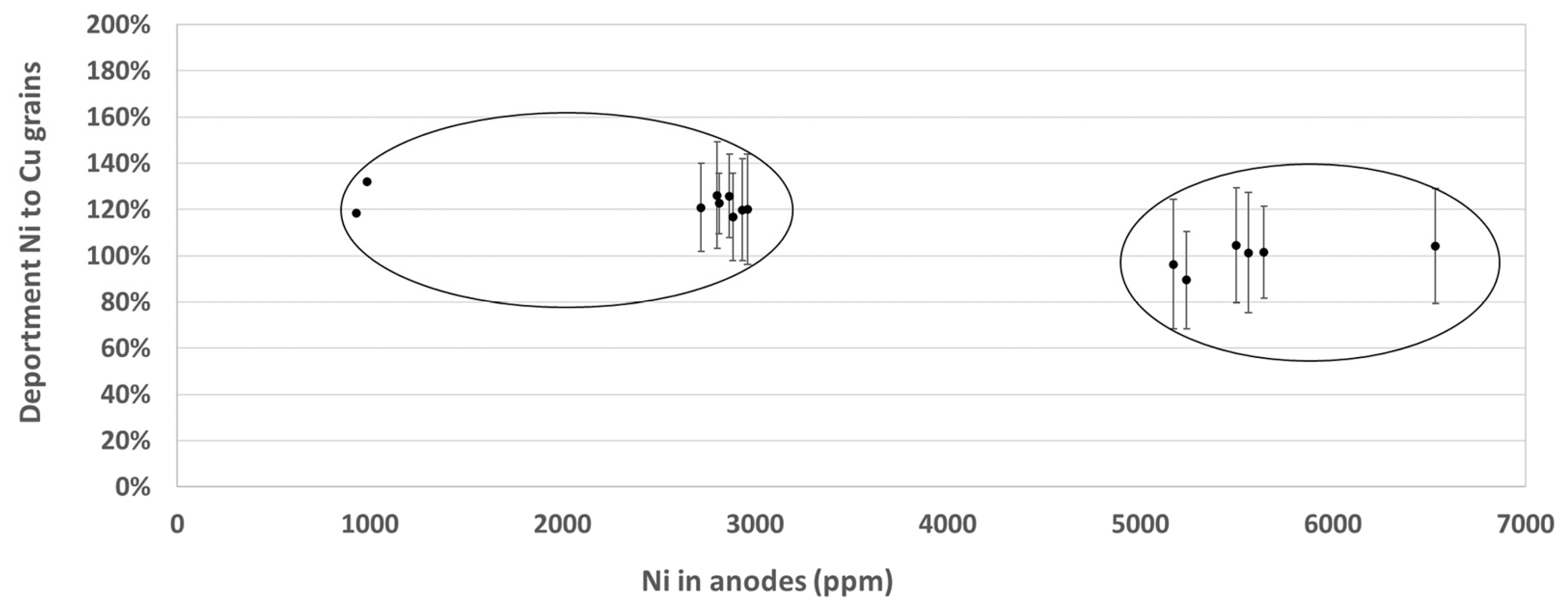
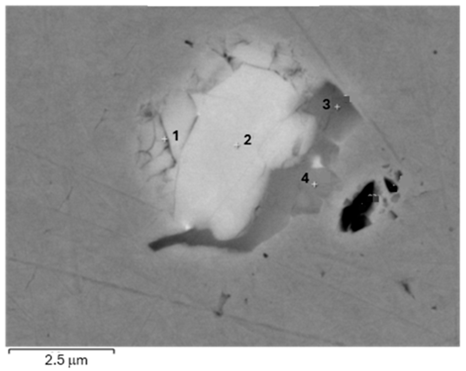
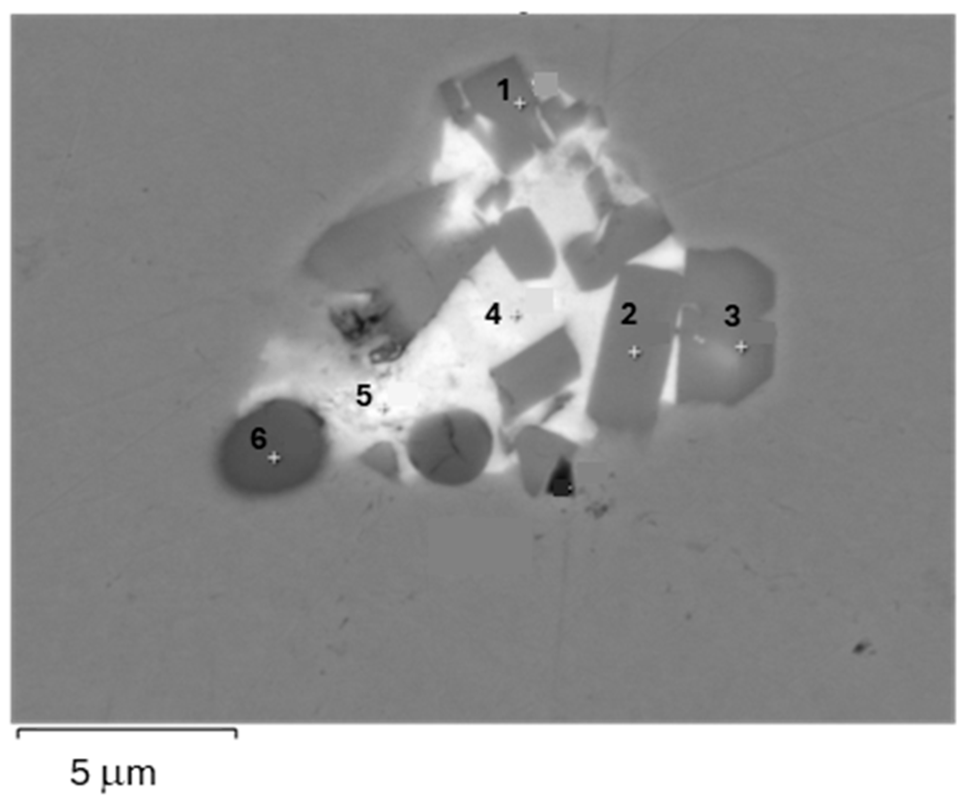
3.2. Chemical Distribution of Impurities in Cu Grains

EPMA analysis (Figure 2) was performed to examine the impurity content within Cu grains of the two commercial anodes (AC1 and AC2) and the doped anodes (DA). Thirty Cu grains were analyzed for the solid solution impurity content for each anode. The results of the analysis are shown in the Supplementary Materials (Table S2). Of the elements studied, Ni, As, Ag and Sn were detected in solid solution at measurable quantities (Table 2). Ni concentrations in Cu grains as measured by EPMA were in most cases higher than bulk Ni analyzed by OES. This was observed by other authors but not discussed [28]. It appears that the method employed in EPMA does not adequately account for matrix effects when measuring low concentrations of nickel (<1 wt.%) in copper grains.
Figure 3 shows the ratio of the measured concentration of Ni in Cu grains by EPMA to measured bulk concentration of Ni in anodes by OES. When the nickel concentration is less than 3000 g/t (0.3 wt.%), the percentage of Ni found in the Cu grains is similar for the commercial anodes from Atlantic Copper and the doped anodes. For anodes that had Ni concentrations of 5000–6000 g/t, a reduction of ca. 20% in the deportment of Ni to the Cu grains was observed. Previous studies established that when Ni concentrations in anodes were above 2500–3000 g/t, NiO and Kupferglimmer were found along Cu grain boundaries [35,36]. Thus, the nickel not contained in the copper grains in this study are expected to be found in nickel-bearing inclusions like NiO and Kupferglimmer.
Arsenic was measured above its detection limit for some Cu grains. For this analysis, in copper grains with measured As concentrations less than the limit of detection, it was assumed that no arsenic was present in those Cu grains. This produced a conservative estimate of solid solubility. Arsenic distribution depends on its concentration in anodes. For anodes with <1000 g/t As, 40% of the arsenic reported to the solid solution, while anodes with >1000 g/t As had 60% of their arsenic found in solid solution with the copper grains. Another work found ca. 30% of anode arsenic content within Cu grains [27].
Tin was found above its detection limit in some Cu grains. Like arsenic, when Sn concentration was below the limit of detection, it was assumed no tin was present in solid solution. The deportment of Sn to the Cu grains also depends on its concentration. Roughly 32% of the Sn reported to the Cu grains in anodes with Sn concentrations from 300 to 400 g/t. A previous study examined anodes with <400 g/t Sn and found a similar deportment of 30% to solid solution as the current study [19]. For anodes with Sn concentrations higher than 700 g/t, only ca. 9% reported to Cu grains. This indicated that increasing Sn concentration from 400 g/t to 700 g/t led to the formation of more tin-bearing inclusions.
Sb concentrations of all Cu grains examined were below the detection limit of EPMA. Sb was only found in complex oxide inclusions and Kupferglimmer. In a previous study, 20 % of the total Sb was found in solid solution [37]. A Sb content > 0.01 wt. % causes a spheroidization of Cu2O inclusions, as shown in Figure 4 [27].

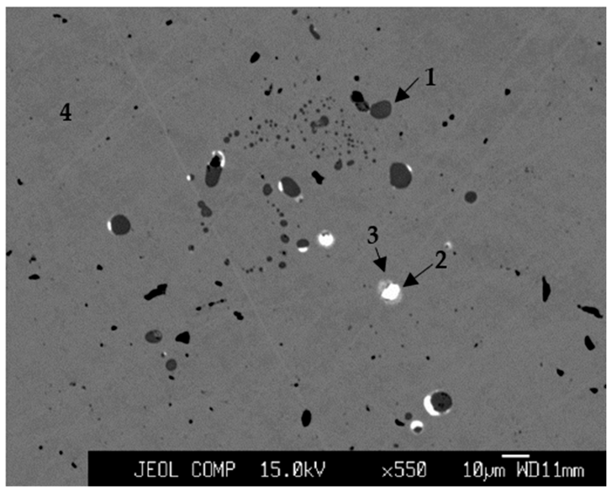
3.3. Chemical Distribution of Impurities in Inclusions

SEM (Figure 4) and EPMA of commercial anode samples identified three predominant inclusion phases: (i) copper (I) oxide, (ii) a complex oxide mainly containing Cu and Pb with minor amounts of As, Sb, Bi, and (iii) copper selenide with traces of Ag and Te (Table 3).
In SEM images, Cu2O appears as small dark particles along grain boundaries and eutectic areas at grain corners (Figure 4, point 1). This phase was analyzed as 88.8 wt% Cu and 11.2 wt% O, which are the expected values for Cu2O. The size of the inclusions varies from <1 to 20 µm. The shapes of the oxides were elongated or circular. This phase compound has been extensively described by Chen and Dutrizac, who also reported diameters from less than 1 µm up to 10 µm [28], 15 µm [20] and 20 µm [38]. Cu2O is an important compound to consider during electrorefining as it dissolves chemically and results in increased copper concentrations in the electrolyte. Elevated copper concentrations increase the electrolyte density and the risk of anode passivation if the electrolyte concentration of Cu + Ni is greater than 65 g/L [39].
Complex oxide particles appear white in backscatter SEM images due to the high atomic mass of lead in the phase (Figure 4, point 2). The diameters of the complex oxides varied from 2 to 15 µm, which again is like previous studies [20]. This phase occurs as inclusions along Cu grain boundaries. No differences were detected between complex oxides that formed near the center of the anode and those that formed near the anode surface. The composition of the complex oxide was highly variable, with Pb ranging from 10 to 70 wt%. On the other hand, Cu, As, Sb and Bi represented less than 20 wt% individually in most complex oxides. This composition variability has been mentioned by Chen and Dutrizac, although, in their studies, one or two of the Group 15 constituents were absent in some of the complex oxides [20].
The selenide phase appears as grey rings in the backscatter SEM image, encircling partially both the complex oxide and the Cu2O oxide phases (Figure 4, point 3). The cross-section thickness of the ring structures was found to be typically 1–2 µm. Selenide phase compositions varied depending on the area analyzed. Cu ranged from 60 to 66 wt%, Se from 30 to 35 wt%, Ag from 0.1 to 0.5 wt% and Te from 3 to 4 wt%. Previous research had found that Ag substitutes for Cu, and Te for Se, forming (Cu, Ag)2(Se, Te) inclusions [28], which seems to be confirmed by this study. Se and Te are not expected to be detected in solid solution by EPMA, as the solubility of Se in copper at 500 °C is believed to be less than 3 g/t [40].
The surface area of inclusions in the EPMA images was determined using Image J image analysis software v. 1.54g. The number of pixels which were a different shade of gray than the copper matrix was counted. Then, the percentage of the area covered by the inclusion was calculated using the counted pixels and the total number of pixels. The surface area, which represents the volume of inclusions in the anodes studied, was 2% to 5%.
Examination of the doped anodes (Figure S4) revealed that increasing impurity content resulted in a decrease in the formation of Cu2O both along the grain boundaries and as eutectic formations. This was especially observed for doped anodes with high concentrations of Ni, which had the lowest levels of Cu2O. The presence of Cu2O inclusions was clearly seen as darker gray circular areas along grain boundaries in the AC1 sample (see Figure 5a). Cu2O inclusions were almost nonexistent in the doped anodes with high levels of impurities (see Figure 5b).
This can be explained due to the increase in impurities (e.g., Sn, As, Sb, Pb and Ni) with higher affinities for oxygen than Cu. These differences in oxide stability are shown in the Ellingham diagram presented in Figure 6. At the refining furnace temperature (ca. 1250 °C), oxide compounds with a lower ΔGf than the ΔGf for Cu2O are more likely to form. This resulted in a decrease in the amount of Cu2O formed as the anode solidified. The oxides formed are not dissolved in Cu grains, but form inclusions in the doped anodes. These new inclusions, which are not found in commercial anodes, corresponded to (i) SnO2, (ii) NiO and (iii) a complex Cu-Ni-Sb-Sn oxide called Kupferglimmer.
As discussed previously, Sn is mainly found in inclusions and not in solid solution within the copper grains. To examine the different species within complex oxide clusters, FESEM was employed instead of EPMA due to the equipment’s higher spatial resolution. In the commercial anodes, no SnO2 was found by FESEM because of the low concentration of tin in the anodes. SnO2 was observed in doped anodes as either euhedral free crystals or clustered with complex oxide inclusions (see Figure 7). This type of inclusion was present in all the doped anodes.
The SnO2 phase exhibited a consistent composition of 70 wt% Sn and 30 wt% O, which is similar to the expected values of 79 wt% Sn and 21 wt% O. These inclusions had a size of ca. 5 µm, which is within the range presented in a previous study [19].
In the electrorefining process, Sn present in Cu grains will react with the electrolyte and precipitate as anode slime. On the other hand, SnO2 in the anode will fall as slimes to the bottom of the cell and not dissolve into the electrolyte [19]. Thus, increasing tin in anodes will likely cause more tin oxide in refining slimes.
NiO was observed in doped anodes as discrete circular inclusions or as part of the complex oxide clusters, as shown in the FESEM image in Figure 8. NiO composition was measured at 70 wt% Ni and 30 wt% O, which is similar to the expected values of 79 wt% Ni and 21 wt% O. All NiO inclusions were less than 3 µm in size. According to the literature, NiO forms in anodes when the Ni concentration is higher than 2500 g/t [36]. The NiO phase does not readily dissolve during electrorefining and deports to the slimes [41].
NiO was only found in the doped anodes with Ni concentrations between 5200 and 6500 g/t. In this work, it appeared that all NiO in the doped anodes with lower concentrations of Ni (2700–2900 g/t) reacted with Cu2O, Sb2O5 and SnO2 to form Kupferglimmer. This seems to indicate that Kupferglimmer formation is limited in commercial anodes by the quantity of Sb and Sn present in the melt. This statement reinforces the results by Chen and Dutrizac [35], who commented that Kupferglimmer formation also depends on the Sb content in the anode.
Kupferglimmer is a complex copper nickel oxide phase that has been described in the literature as Cu3Ni2−xSbO6−x, where x = 0.1–0.2 [20]. Kupferglimmer occurs either as euhedral crystals or grouped with other complex oxide phases, such as SnO2 and NiO (Figure 7, points 3–4; Figure 8, points 1–3). Chen and Dutrizac reported that Kupferglimmer was found around a core of NiO [34]. This was not observed in this research. These inclusions have a size below 5 µm. In previous studies, Kupferglimmer was found as platelets with a size up to 10 µm [35] and from 2 to 15 µm [20]. This compound is formed in the molten phase by reacting Cu2O, Sb2O5, SnO2 and NiO [35]. It is considered as a refractory slime compound, as it is difficult to leach and results in a loss to Cu recovery during slime processing [35].
Kupferglimmer was present in all doped anodes regardless of Ni concentration (Ni 2700–6500 g/t), Sb (430–930 g/t) and Sn (305–829 g/t). Previous research indicated that concentrations of Ni and Sb needed to be above 3000 g/t and 200 g/t, respectively, in anodes for Kupferglimmer to form [35]. This work indicates that Kupferglimmer can form at nickel concentrations as low as 2700 g/t.
While Kupferglimmer was detected in all doped anodes, NiO was only observed with doped anodes at the higher level studied (5200–6500 g/t Ni). To examine this phenomenon, the available nickel, antimony and tin for Kupferglimmer formation were calculated by subtracting 2500 g/t Ni, 200 g/t Sb and 100 g/t Sn from each anode composition. The Ni and Sb values were selected based on the amount needed to form Kupferglimmer, as indicated by Forsen et al. [36,41,42] and Chen and Dutrizac [20], respectively. The tin value was selected based on this study’s Sn concentration found in solid solution in copper grains. From the available amount, the number of moles per ton available for Kupferglimmer formation were calculated. Using a molar stoichiometry of 2 Ni to 1 (Sb + Sn), it was calculated that excess Sb and Sn were present to form Kupferglimmer with all available nickel for all doped anodes that did not have NiO present. For doped anodes where NiO was detected, an excess of nickel was calculated, indicating that all Sb and Sn were consumed. Thus, it appears that Kupferglimmer likely formed at the expense of NiO if enough Sb and Sn were present during anode casting.
In the present study, Kupferglimmer was found to contain Sn (Figure 9). This happened for all anodes regardless of Sn content (300 to 800 g/t). The presence of Sn in Kupferglimmer was mentioned in previous studies [20,35], although the concentrations of Sn in the anodes were not reported.
The concentration of Sn in Kupferglimmer depended on the anode’s Sn concentration. The Sn content in Kupferglimmer varied from 8 to 12 wt% in anodes with 300–400 g/t Sn to 15–24% for anodes with 700–800 g/t Sn. This result indicates that the amount of SnO2 reacting with Cu2O, Sb2O5 and NiO depended on the Sn content of the anode.

4. Conclusions

The present study characterized commercial Cu refining anodes and doped anodes created in a laboratory to resemble possible compositions created in a combination primary/secondary smelter. The Cu anodes doped with Ni, Sn, and Sb simulate potential anode materials created by the recycling of electronic scrap in a circular economy. These impurities deported between the Cu grains and inclusions decorating the Cu grain boundaries.
Electron microscope analyses (EPMA and FESEM) showed that Ni reported mainly to Cu grains as a solid solution impurity, with a minor amount deported to inclusions. In anodes with high Ni concentration (ca. 6000 g/t), it was estimated that 20% of the Ni content was found in inclusions of NiO and Kupferglimmer. NiO was not found in anodes with 2500–2700 g/t Ni, but Kupferglimmer was found in these materials. This indicated that the formation of Kupferglimmer is preferred to NiO and is limited by the availability of antimony and tin. Kupferglimmer was found to be more enriched in Sn when anodes had higher tin content over the range studied (300–900 g/t Sn).
Arsenic was present both within Cu grains and complex oxide inclusions. The deportment of As to Cu grains depends on its concentration in an anode. Approximately 40% of As was found in solid solution in anodes with <1000 g/t As, while ca. 60 % was in solid solution for anodes with >1000 g/t As. Arsenic was present in complex oxide phases with Pb, Cu, Sb and Bi.
Sb was present both in complex oxides and Kupferglimmer. Antimony competed with Sn in Kupferglimmer formation.
Sn was present both in Cu grains and as oxide inclusions. The deportment of Sn to Cu grains depended on its concentration in anodes. Ca. 32% of Sn was found in solid solution for anodes with 300–400 g/t Sn and ca. 9 % for anodes with 700–800 g/t Sn. Sn was present either as SnO2 or within Kupferglimmer. Higher concentrations of antimony and tin increased the likelihood of Kupferglimmer formation and depressed NiO creation.
These results highlight the possible changes expected in the chemical composition of Cu anodes as our society moves to a more circular economy. Anodes will likely contain more impurities and the presence of Kupferglimmer, NiO and SnO2 in slimes will increase.
The impact of the higher impurity concentrations in the anodes provided by WEEE and the phases formed will affect the electrorefining process in terms of Ni deportment, Kupferglimmer generation, and the properties of electrolyte and slimes. Ni in Cu grains will accumulate in the electrolyte, affecting its conductivity and viscosity, and may lead to anode passivation. NiO will accumulate in the slimes, increasing slime production per ton of anode. Kupferglimmer may decrease current efficiency because of slime entrapment in the cathode. As Kupferglimmer is a refractory material, the recovery of its Cu content during slime processing will be difficult. The study of these potential changes in the electrorefining of doped anodes deserves further research.

Supplementary Materials

The following supporting information can be downloaded at: https://www.mdpi.com/article/10.3390/met15020113/s1, Figure S1: Anode block received for cutting into pieces; Figure S2: Anode block design for cutting into pieces. Blue rectangular pieces were used for electrorefining. Yellow round pieces were used for OES analysis. Green rectangular pieces were used to analyze the internal structure of the anodes by EPMA, FESEM and Optical microscopy. Purple round piece was employed for O2 analysis by ELTRA; Table S1: Sanding and polished steps for probes analyzed by Microscopy; Figure S3: Probe generated for Electron Microscopy analysis (left) and after etching (right) with 100 mL H2O, 25 mL HCl 37% and 5 g FeCl3 for grain size analysis by Optical Microscopy; Figure S4: Backscattered electron micrograph showing the general structure of doped anodes. (A) DA1; (B) DA2; (C) DA3; (D) DA4; (E) DA5; (F) DA6; (G) DA7; (H) DA8; (I) DA9; (J) DA10; (K) DA11; (L) DA12; (M) DA13; Table S2: Impurity content in solid solution (wt. %) of commercial (AC1 and AC2) and doped (DA1 to DA13) anodes. 30 Cu grains were analyzed for each doped anode. For the rest of the elements, only maximum values are shown, as minimum values and means are below the limits of detection (LD), are in wt.%: As 0.05; Ni 0.04; Sb 0.03; Sn 0.04.

Author Contributions

Conceptualization, G.R., D.S.-R. and M.S.M.; methodology, D.S.-R. and M.S.M.; validation, A.M.-A.; investigation, A.M.-A.; writing—original draft preparation, A.M.-A.; writing—review and editing, D.S.-R. and M.S.M.; supervision, G.R., D.S.-R. and M.S.M.; funding acquisition G.R. All authors have read and agreed to the published version of the manuscript.

Funding

This research was funded by University of Huelva grant number 2019.

Data Availability Statement

The original contributions presented in this study are included in the article. Further inquiries can be directed to the corresponding author.

Acknowledgments

A.M.-A. acknowledges financial support from University of Huelva under Call Grants for Industrial Doctoral Studies (2019).

Conflicts of Interest

Authors Agustin Morales-Aragon and Guillermo Ríos are employed by the company Atlantic Copper SLU. Author G.R. is employed by the company Atlantic Copper SLU. The remaining authors declare that the research was conducted in the absence of any commercial or financial relationships that could be construed as a potential conflict of interest.

References

  1. Reuter, M.A.; Van Schaik, A.; Gutzmer, J.; Bartie, N.; Abadías-Llamas, A. Challenges of the Circular Economy: A Material, Metallurgical, and Product Design Perspective. Annu. Rev. Mater. Res. 2019, 49, 253–274. [Google Scholar] [CrossRef]
  2. Salviulo, G.; Lavagnolo, M.C.; Dabalà, M.; Bernardo, E.; Polimeno, A.; Sambi, M.; Bonollo, F.; Gross, S. Enabling Circular Economy: The Overlooked Role of Inorganic Materials Chemistry. Chem.-A Eur. J. 2021, 27, 6676–6695. [Google Scholar] [CrossRef] [PubMed]
  3. MacArthur, E. Towards the Circular Economy: Opportunities for the Consumer Goods Sector; Ellen MacArthur Foundation: Cowes, UK, 2013; ISBN 0102603022. [Google Scholar]
  4. IEA Global Critical Minerals Outlook 2024. Available online: https://www.iea.org/reports/global-critical-minerals-outlook-2024?utm_content=buffer3599f&utm_medium=social&utm_source=linkedin.com&utm_campaign=buffer (accessed on 1 December 2024).
  5. Elshkaki, A.; Graedel, T.E.; Ciacci, L.; Reck, B.K. Resource Demand Scenarios for the Major Metals. Environ. Sci. Technol. 2018, 52, 2491–2497. [Google Scholar] [CrossRef] [PubMed]
  6. Pietrzyk, S.; Tora, B. Trends in global copper mining—A review. In Proceedings of the IOP Conference Series: Materials Science and Engineering; IOP Publishing: Bristol, UK, 2018; Volume 427. [Google Scholar]
  7. Ciacci, L.; Fishman, T.; Elshkaki, A.; Graedel, T.E.; Vassura, I.; Passarini, F. Exploring future copper demand, recycling and associated greenhouse gas emissions in the EU-28. Glob. Environ. Chang. 2020, 63, 102093. [Google Scholar] [CrossRef]
  8. Zhang, J.; Hua, P.; Krebs, P. The build-up dynamic and chemical fractionation of Cu, Zn and Cd in road-deposited sediment. Sci. Total Environ. 2015, 532, 723–732. [Google Scholar] [CrossRef]
  9. ICSG. The World Copper Factbook 2020; ICSG: Lisbon, Portugal, 2020; ISBN 9780874216561. [Google Scholar]
  10. Lennartsson, A.; Engström, F.; Samuelsson, C.; Björkman, B.; Pettersson, J. Large-Scale WEEE Recycling Integrated in an Ore-Based Cu-Extraction System. J. Sustain. Metall. 2018, 4, 222–232. [Google Scholar] [CrossRef]
  11. Loibl, A.; Tercero Espinoza, L.A. Current challenges in copper recycling: Aligning insights from material flow analysis with technological research developments and industry issues in Europe and North America. Resour. Conserv. Recycl. 2021, 169, 105462. [Google Scholar] [CrossRef]
  12. Siegmund, S.M.S.D.A. Challenges and opporunities with WEEE treatment in Cu smelting processes. In Proceedings of the Copper 2022, Santiago de Chile, Chile, 13–17 November 2022; pp. 17–33. [Google Scholar]
  13. Van Yken, J.; Cheng, K.Y.; Boxall, N.J.; Sheedy, C.; Nikoloski, A.N.; Moheimani, N.R.; Kaksonen, A.H. A comparison of methods for the characterisation of Waste-Printed Circuit Boards. Metals 2021, 11, 1935. [Google Scholar] [CrossRef]
  14. Ohtsuka, T.T.H.S.K.A.N. Development of physical separation process of Electronic Scrap for copper smelting and refining. In Proceedings of the Copper International Conference 2022, Santiago de Chile, Chile, 13–17 November 2022; Volume 9, pp. 45–57. [Google Scholar]
  15. Fountain, C. The Whys and Wherefores of Penalty Elements in Copper Concentrates. In Proceedings of the MetPlant 2013: Metallurgical Plant Design and Operating Strategies, Perth, Australia, 15–17 July 2013. [Google Scholar]
  16. Nakawara, K.W.S. The behavior of impurities at Kosaka Smelter. In Proceedings of the Metallurgical and Materials Processing: Principles and Technologies; The Minerals, Metals and Materials Society: Pittsburgh, PA, USA, 2003; Volume II, pp. 521–531. [Google Scholar]
  17. Schlesinger, M.E.; Sole, K.C.; Davenport, W.G.; Flores, G.R. Extractive Metallurgy of Copper; Elsevier: Amsterdam, The Netherlands, 2023; ISBN 2013206534. [Google Scholar]
  18. Adam, F.; Wood, J.; Andrews, R. Processing of Electronic Scrap with Ausmelt TSL Technology. In E3S Web of Conferences; EDP Sciences: Les Ulis, France, 2024; Volume 543, pp. 4–9. [Google Scholar] [CrossRef]
  19. Chen, T.T.; Dutrizac, J.E. A mineralogical study of the deportment of impurities during the electrorefining of secondary copper anodes. In Proceedings of the Copper 99-Cobre 99 International Conference; Dutrizac, J.E., Ji, J., Ramachandran, V., Eds.; The Minerals, Metals and Materials Society: Pittsburgh, PA, USA, 1999; Volume 111, pp. 437–460. [Google Scholar]
  20. Chen, T.T.; Dutrizac, J.E. Mineralogical characterization of anode slimes: Part v-nickel-rich copper anodes from the ccr division of noranda minerals inc. Can. Metall. Q. 1990, 29, 27–37. [Google Scholar] [CrossRef]
  21. Miyamoto, M.; Mitsuno, S.; Kitada, A.; Fukami, K.; Murase, K. Mechanism of nodular growth in copper electrorefining with the inclusion of impurity particles under natural convection. Hydrometallurgy 2023, 216, 106013. [Google Scholar] [CrossRef]
  22. Mori, K.; Yamakawa, Y.; Oue, S.; Taninouchi, Y.K.; Nakano, H. Effect of Impurity Ions and Additives in Solution of Copper Electrorefining on the Passivation Behavior of Low-Grade Copper Anode. Mater. Trans. 2023, 64, 242–251. [Google Scholar] [CrossRef]
  23. Miyamoto, M.; Ishikawa, Y.; Fukami, K.; Murase, K. Surface Roughening and Growth-Promoting Effects of Nickel and Antimony on Nodules in Copper Electrorefining. Metall. Mater. Trans. B 2023, 54, 3579–3590. [Google Scholar] [CrossRef]
  24. Markovic, R.; Krstic, V.; Friedrich, B.; Stopic, S.; Stevanovic, J.; Stevanovic, Z.; Marjanovic, V. Electrorefining process of the non-commercial copper anodes. Metals 2021, 11, 1187. [Google Scholar] [CrossRef]
  25. Sahlman, M.; Aromaa, J.; Lundström, M. Detachment and flow behaviour of anode slimes in high nickel copper electrorefining. Physicochem. Probl. Miner. Process. 2024, 60, 186194. [Google Scholar] [CrossRef]
  26. Djokić, J.; Radovanović, D.; Nikolovski, Z.; Andjić, Z.; Kamberović, Ž. Influence of electrolyte impurities from e-waste electrorefining on copper extraction recovery. Metals 2021, 11, 1383. [Google Scholar] [CrossRef]
  27. Wenzl, C. Structure and Casting Technology of Anodes in Copper Metallurgy. Ph.D. Thesis, University of Leoben, Leoben, Austria, 2008. [Google Scholar]
  28. Chen, T.T.; Dutrizac, J.E. Mineralogical characterization of anode slimes-i. anode copper from inca’s copper cliff copper refinery. Can. Metall. Q. 1988, 27, 91–96. [Google Scholar] [CrossRef]
  29. Marković, R.; Friedrich, B.; Stajić-Trošić, J.; Jordović, B.; Jugović, B.; Gvozdenović, M.; Stevanović, J. Behaviour of non-standard composition copper bearing anodes from the copper refining process. J. Hazard. Mater. 2010, 182, 55–63. [Google Scholar] [CrossRef]
  30. Möller, C.A.; Bayanmunkh, M.; Friedrich, B. Influence of As, Sb, Bi and O on copper anode behaviour—Part 1: Passivation characteristics. World Metall.-Erzmetall 2008, 61, 357–367. [Google Scholar]
  31. Möller, C.A.; Bayanmunkh, M.; Friedrich, B. Influence of As, Sb, Bi and O on copper anode behaviour—Part 2: Anode dissolution behaviour and anode sludge generation. World Metall.-Erzmetall 2009, 62, 6–16. [Google Scholar]
  32. Möller, C.A.; Bayanmunkh, M.; Friedrich, B. Influence of As, Sb, Bi and O on copper anode behaviour—Part 3: Elemental distribution. World Metall.-Erzmetall 2009, 62, 70–80. [Google Scholar]
  33. Dupont, D.; Arnout, S.; Jones, P.T.; Binnemans, K. Antimony Recovery from End-of-Life Products and Industrial Process Residues: A Critical Review. J. Sustain. Metall. 2016, 2, 79–103. [Google Scholar] [CrossRef]
  34. Mitan, M. Microstructure and Morphology of Impure Copper Anodes. Ph.D. Thesis, University of Arizona, Tucson, AZ, USA, 1997. [Google Scholar]
  35. Chen, T.T.; Dutrizac, J.E. Mineralogical characterization of anode slimes-iv. copper-nickel-antimony oxide (“kupferglimmer”) in ccr anodes and anode slimes. Can. Metall. Q. 1989, 28, 127–134. [Google Scholar] [CrossRef]
  36. Forsén, O. The Behaviour of Arsenic, Antimony and Bismuth in the Solidification and Electrolysis of Nickel-Oxygen-Bearing Copper Anodes; The Minerals, Metals and Materials Society: Pittsburgh, PA, USA, 1985; pp. 353–377. [Google Scholar]
  37. Chen, T.T.; Dutrizac, J.E. Mineralogical characterization of a copper anode and the anode slimes from the La Caridad copper refinery of Mexicana de Cobre. Metall. Mater. Trans. B 2005, 36, 229–240. [Google Scholar] [CrossRef]
  38. Chen, T.T.; Dutrizac, J.E. Mineralogical characterization of anode slimes: Part 7-copper anodes and anode slimes from the chuquicamat a division of codelco-Chile. Can. Metall. Q. 1991, 30, 95–106. [Google Scholar] [CrossRef]
  39. Kurimoto, K.; Aoki, H.; Yamaguchi, Y.; Hattori, Y. High current density operation at the toyo tank house #2. In Proceedings of the Copper 2016, Kobe, Japan, 13–16 November 2016; Volume EL2-4, pp. 2001–2012. [Google Scholar]
  40. Tayler, P.L.; Van Wagoner, D.L.; Pitt, C.H. Solubility limits of selenium in copper. Metall. Trans. B 1976, 7, 103–106. [Google Scholar] [CrossRef]
  41. Forsén, O. Solidification and Electrolysis of Copper Anodes Containing Nickel, Arsenic, Antimony and Bismuth; The Minerals, Metals and Materials Society: Pittsburgh, PA, USA, 1987; pp. 47–69. [Google Scholar]
  42. Forsen, O.; Tikkanen, M.H. On the dissolution of Copper Anodes in Electrolytic Refining Part I: The behaviour of nickel in oxygen-bearing copper anodes. Scand. J. Metall. 1981, 10, 109–114. [Google Scholar]
Figure 1. Optical micrograph showing the distribution of the Cu grain: (a) commercial anode; (b) doped anode.
Metals 15 00113 g001
Figure 2. Backscattered electron micrograph showing the general structure of a commercial anode (AC1). The large black shapes are casting voids found in the specimen.
Metals 15 00113 g002
Figure 3. Ni deportment in Cu grains at low doped (ca. 3000 g/t) and high doped (ca. 5000–6500 g/t) Ni concentration in anodes. Error bars correspond to standard deviation.
Metals 15 00113 g003
Figure 4. Backscattered electron micrograph showing the general structure of an AC1. 1—Cu2O, 2—CuPbAsBiSb oxide, 3—(Cu, Ag)2(Se,Te),4—Cu grain.
Metals 15 00113 g004
Figure 5. Backscattered electron micrograph showing the general structure of two anodes: (a) anode AC1; (b) anode DA13.
Metals 15 00113 g005
Figure 6. Ellingham diagram for common metal oxides that can form during copper anode solidification. Solid lines correspond to condensed metals and oxides. Dashed lines correspond to condensed metals and gaseous oxide.
Metals 15 00113 g006
Figure 7. Backscattered electron micrograph showing the structure of the inclusions in doped anodes. 1–2—SnO2; 3–4—Kupferglimmer.
Metals 15 00113 g007
Figure 8. Backscattered electron micrograph showing the structure of the inclusions in doped anodes. 1–3—Kupferglimmer; 4–5—complex lead copper oxide; 6—NiO.
Metals 15 00113 g008
Figure 9. Sn deportment in Kupferglimmer at low doped (300–400 g/t) and high doped (700–800 g/t) Sn concentrations in anodes. Error bars correspond to standard deviation.
Metals 15 00113 g009
Table 1. Chemical composition of the commercial (AC1 and AC2) and doped (DA1 to DA13) anodes (in g/t). The limits of detection (g/t) of metals and metalloids by OES are Ni 0.7, Sn 0.1, Sb 0.8, As 0.6, Ag 1.3, Bi 0.7, Pb 1.7, Se 0.2, Te 0.5.
AnodeNiSnSbAsOAgBiPbSeTe
AC19291131948611545300250110639660
AC2985301591744113530234039735552
DA129623244818431944254364107237258
DA2281334259369821002193851135505109
DA328043555011508 a157620525896031245
DA45562 a306457783163025131491936653
DA55241 a3054295861900209392996480108
DA62885360741 a8422070268366101537056
DA72935690 a477831213426936197037459
DA82868748 a5207581466244504107835849
DA92721744 a709 a6172203207437926480117
DA105643 a3985261555 a152221529690434050
DA115500 a395753 a8152036255336103135855
DA125172 a769 a930 a68420262365141005531127
DA136533 a829 a881 a1466 a1543200696116230843
a Higher concentration levels of Ni, Sn, Sb and As for doped anodes.
Table 2. Analyses of elements found within copper grains in anodes doped at high and low concentration levels, and the calculated percentages of the elements present in solid solution. Bulk concentration determined by OES analysis. A total of 30 Cu grains were analyzed by EMPA for each doped anode.
Low Concentration LevelHigh Concentration Level
ElementConcentration (g/t)Percentage to Solid Solution (%)Concentration
(g/t)
Percentage to
Solid Solution (%)
Ni2900>1005600100
As75540157060
Sn350327509
Sb49008000
Table 3. Phases found in inclusions of commercial (AC) and doped (DA) anodes. AC anodes contain three phases: Cu2O, complex Cu-Pb-As-Sb-Bi oxide and (Cu, Ag)2(Se,Te), labelled together as AC inclusions.
AnodeImpurity Phases
AC1, AC2AC inclusions
DA1AC inclusions + SnO2 + Kupferglimmer
DA2AC inclusions + SnO2 + Kupferglimmer
DA3AC inclusions + SnO2 + Kupferglimmer
DA4AC inclusions + SnO2 + Kupferglimmer + NiO
DA5AC inclusions + Kupferglimmer + NiO
DA6AC inclusions + SnO2 + Kupferglimmer
DA7AC inclusions + SnO2 + Kupferglimmer
DA8AC inclusions + SnO2 + Kupferglimmer
DA9AC inclusions + SnO2 + Kupferglimmer
DA10AC inclusions + SnO2 + Kupferglimmer + NiO
DA11AC inclusions + SnO2 + Kupferglimmer + NiO
DA12AC inclusions + SnO2 + Kupferglimmer + NiO
DA13AC inclusions + SnO2 + Kupferglimmer + NiO
Disclaimer/Publisher’s Note: The statements, opinions and data contained in all publications are solely those of the individual author(s) and contributor(s) and not of MDPI and/or the editor(s). MDPI and/or the editor(s) disclaim responsibility for any injury to people or property resulting from any ideas, methods, instructions or products referred to in the content.

