Article

Deposition of Al Thin Film on Steel Substrate: The Role of Thickness on Crystallization and Grain Growth

1
Department of Inorganic Chemistry, Yerevan State University, 1 A.Manukyan st., Yerevan 0025, Armenia
2
Department of Nano-Optical Engineering, Korea Polytechnic University, Siheung 429-793, Korea
3
Department of Metallurgical & Materials Engineering, Inha Technical College, Incheon 402-752, Korea
4
Department of Renewable Energy, Jungwon University, Goesan-gun, Chungbuk 367-805, Korea
*
Authors to whom correspondence should be addressed.
Metals 2019, 9(1), 12; https://doi.org/10.3390/met9010012
Submission received: 7 November 2018 / Revised: 4 December 2018 / Accepted: 10 December 2018 / Published: 21 December 2018

Abstract

:
In this study, we deposited aluminum (Al) films of different thicknesses on steel substrate and examined their phase, microstructure, and film growth process. We estimated that films of up to 30 nm thickness were mainly amorphous in nature. When the film thickness exceeded 30 nm, crystallization was observed. The further increase in film thickness triggered grain growth, and the formation of grains up to 40 nm occurred. In such cases, the Al film had a cross-grained structure with well-developed primary grains networks that were filled with small secondary grains. We demonstrated that the microstructure played a key role in optical properties. The films below 30 nm showed higher specular reflection, whereas thicker films showed higher diffuse reflections.

1. Introduction

Nano-scaled metal and dielectric materials, and composites of metal–dielectric films, have attracted great interest because of their structural, optical, and electrical properties. Among such materials, aluminum (Al) thin films have been extensively studied, as they are easy to prepare and have novel optical properties [1,2]. Al is also the most abundant metal and the third most abundant element in the earth’s crust, after oxygen and silicon.
A number of techniques have been used to deposit Al films, including RF magnetron sputtering and evaporation, which can employ either thermal or electron beam sources. In general, sputter deposition is more suitable for materials with higher melting points, which are difficult to evaporate. This method has several advantages, including excellent control of film thickness and the fabrication of high-density film.
In addition, the electrical conductivity of Al film is close to ideal bulk values [3], as well as stable and cost-effective. These properties make Al film the ideal choice for an optical scattering layer in optoelectronic devices [4,5]. In general, this structure is formed by thermal annealing using a furnace or rapid thermal equipment following deposition with silver [6]. The physical properties of the Al film strongly depend on its microstructure [7,8]; therefore, by controlling the microstructure, it is possible to govern the film’s properties [9,10,11].
The basic goal of this study was to fabricate Al thin films on steel substrates for flexible devices utilizing a sputtering approach [12,13,14,15]. The growth kinetics, crystallization, and morphology were the main topics of evaluation for this study. In particular, variation in grain size, crystallization degree, and surface roughness depending on film thickness were examined in detail, and they were linked with physical properties.

2. Experimental Details

The Al film was deposited using a sputtering method where the distance between the Al target and substrate was 20 cm. The Al target (Merck, Germany) used was 100 mm in diameter with a purity of 99.9995% and bonded to a Cu-backing plate (155 mm diameter, 6 mm thick). The process pressure was ~1 × 10⁻³ Torr, and the air flow rate in the chamber during deposition was adjusted to 10 sccm. A power of 1000 W was applied to the upper electrode and the lower electrode was grounded at room temperature. The substrate was rotated at 5 rpm to provide a uniform coating. Under these conditions, the deposition rate of the Al material was estimated to be 4.5 Å/s.
Steel plate (chromium steel) with a thickness of 127 µm was used as a substrate because its thermal expansion coefficient (10.5 ppm/K) is lower than that of nickel (Ni)–Cr steel (15.0 ppm/K). The 10 × 10 cm steel plates were carefully cleaned using an organic solvent (acetone and ethyl alcohol), followed by ultra-sonication with de-mineralized water to thoroughly remove grease and organic contamination. Afterwards, the samples were dried with nitrogen. Finally, the Al thin film was deposited on the substrates using the DC sputtering technique.
The crystal structure was examined using the X-ray diffraction (XRD) method with monochromatic CuKα radiation (Rigaku SmartLab, Tokyo, Japan). The microstructure and thickness of the deposited films were evaluated using a scanning electron microscope (SEM) combined with a focused ion beam (Carl Zeiss Merlin, Jena, Germany). An atomic force microscope (AFM) was used to scan the morphologies of the films and the substrate (SPA-300HV SII, Chiba, Japan).

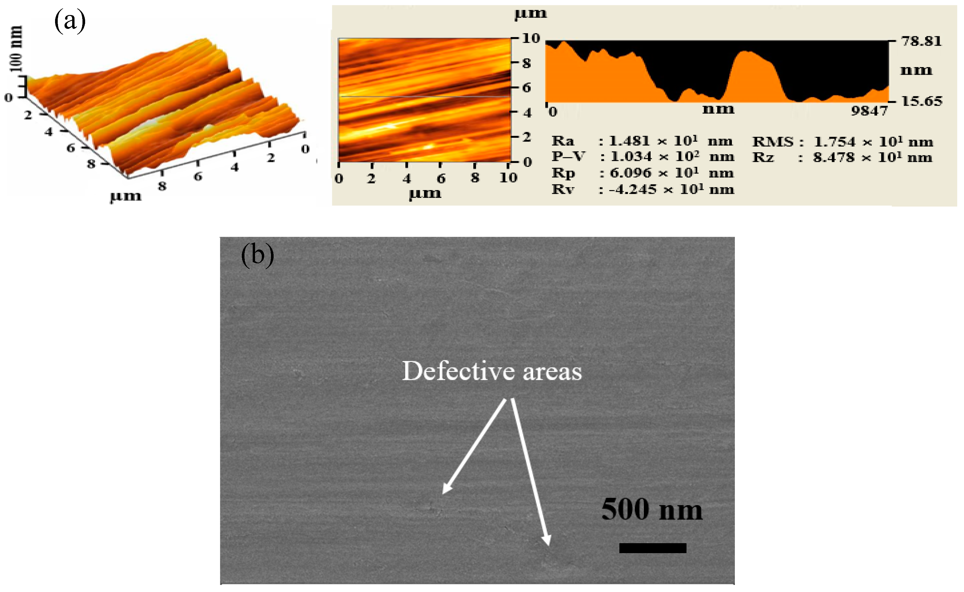
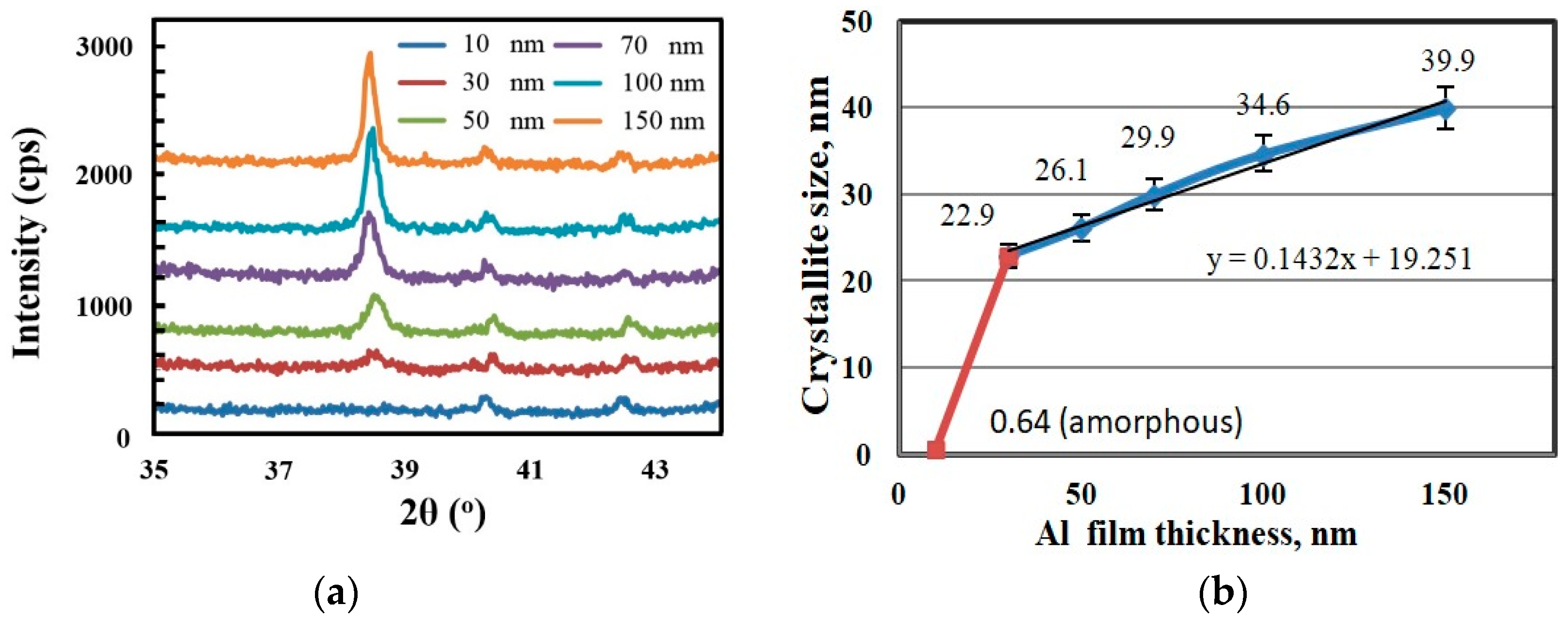
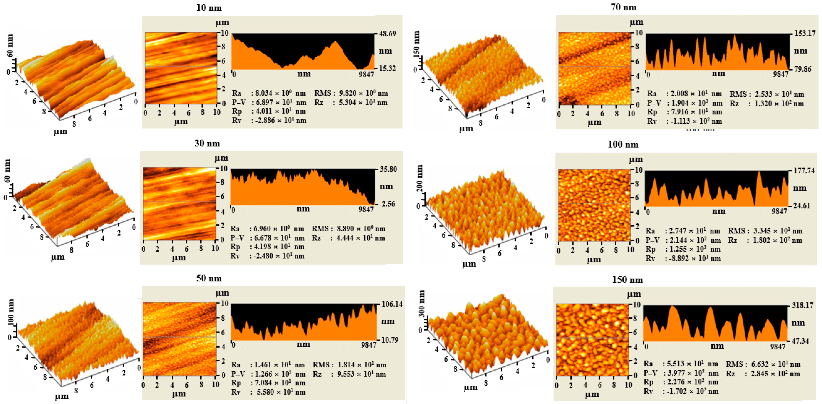
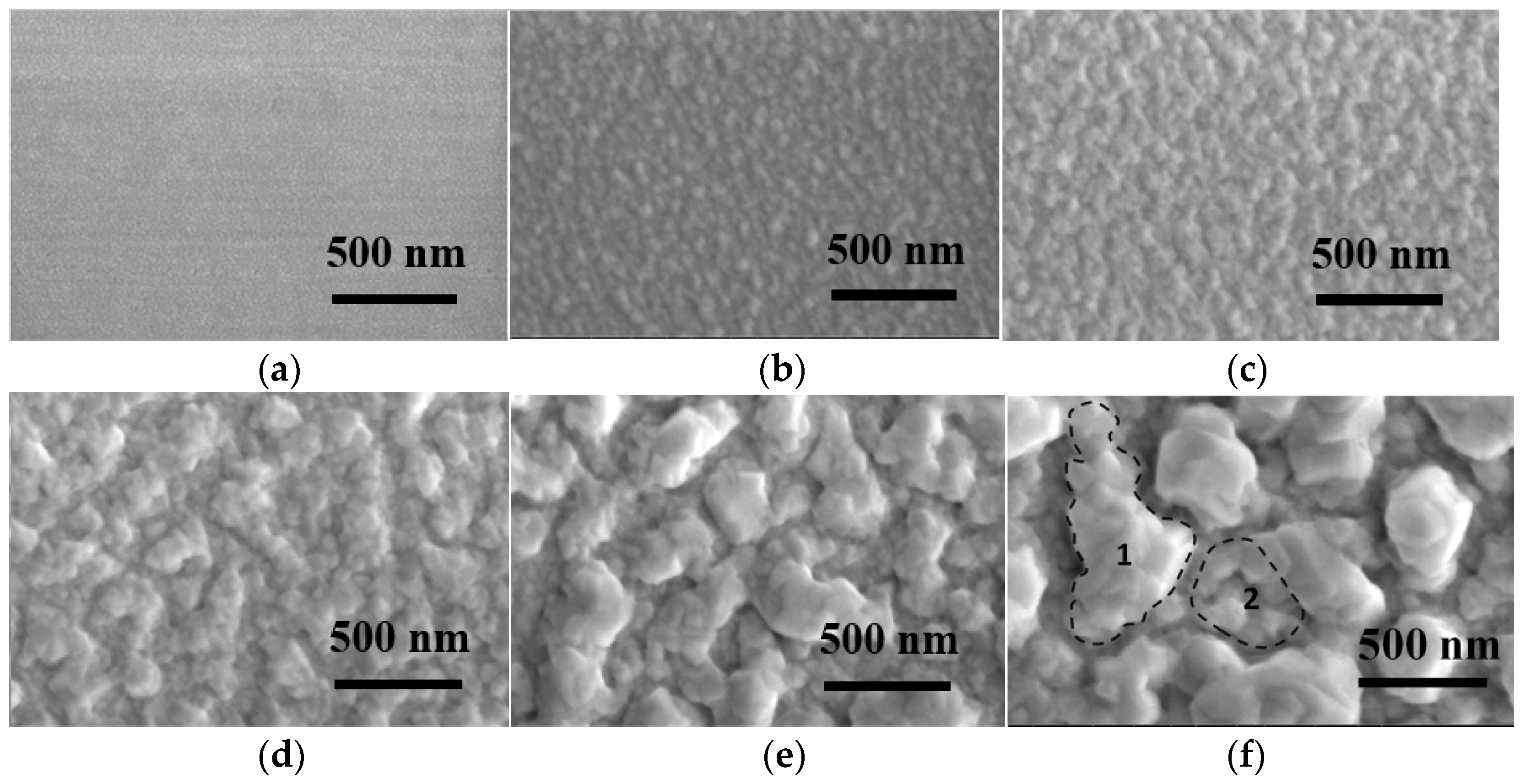
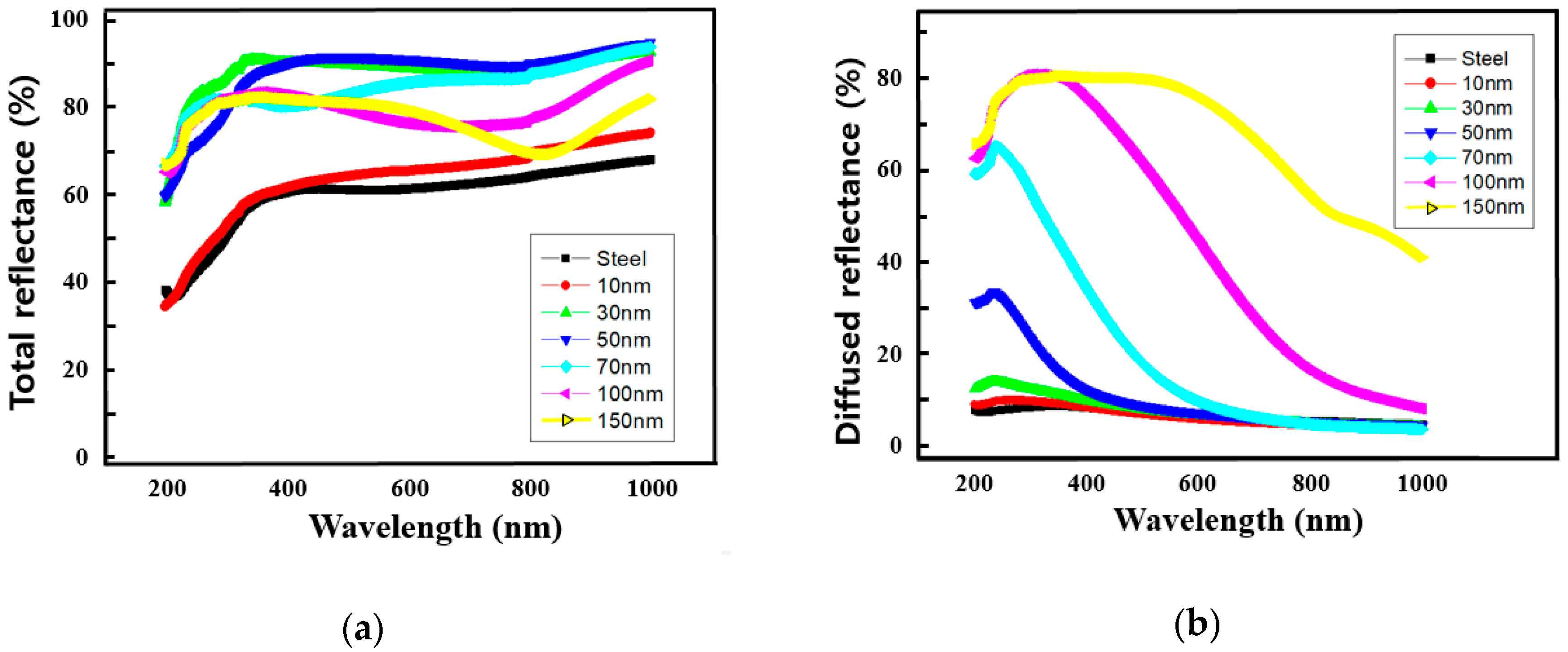
3. Results and Discussion

In addition to the deposition method, the thin film’s growth, structure, and properties also depend on other factors, such as the nature and temperature of the substrate, deposition rate, etc. Defects in the substrate surface morphology may critically influence the film growth process. Therefore, we examined the steel substrate morphology and estimated its root mean square (RMS) roughness to be 18 nm, as illustrated in Figure 1a.
SEM analysis revealed that there were a few defective areas on the top of the steel substrate, however the amount of such defects was not significant (Figure 1b). One could therefore expect that surface roughness would have a minor effect on the deposition process.
In order to estimate the substrate’s effect on film morphology, we deposited an Al film on steel, glass, and silicon wafer and examined their optical properties. The film that was deposited on steel had very low reflecting properties, whereas the surfaces of glass and wafer reflected like a mirror. The images of these three samples on a computer screen, reflecting the microstructure of the Al film, are shown in Figure 2. The silicon wafer, steel, and glass substrates are placed from left to right, respectively. It is clear that the silicon (round wafer) and glass (right rectangular) reflect like a mirror, but the Al film on the steel substrate scatters the light and it has a white hue.
In order to understand the reason for this difference, we need to consider a number of factors, such as the nature of the substrate, substrate temperature, deposition rate, etc., which have a critical influence on the growth, structure, and properties of the deposited thin film. For instance, Garbacz et al. reported that for thin Al films that were deposited on a Ti6Al4V substrate by the evaporation method, the number of pores and cracks were higher when compared to films that were deposited by magnetron sputtering on the same substrate [16]. Mwema et al. reviewed the effect of different parameters on the structure of thin Al films [17]. It was shown that deposition conditions, such as deposition rate [18], alloy composition [19], substrate type, substrate temperature, and roughness [20] had a significant influence on the morphology and structure of the formed film. It was revealed that the structure is sensitive to the deposition technique [14] and film thickness as well.
As indicated, the substrate can also have a critical impact on the film growth process of Al film. The interaction between the substrate and the depositing atoms is one of the key parameters influencing the nucleation process, and the size and structure of islands in the initial stages. Substrates with different origins can have a certain influence on the film formation process.
In Figure 2, the appearances of films deposited on three different substrates, i.e., steel, silicon, and glass, are illustrated. The first substrate was a crystalline metal which has typical metallic bonds, the second was silicon wafer, which is a crystalline metalloid with covalent bonds, and the third substrate was non-crystalline glass having an amorphous structure. The effect of substrate types on the growth process was covered in our previous work [21]. The review [17] and references therein also revealed that substrates may have a critical influence on the morphology of the formed film. Although such a date has been previously published in the literature, there is still a lack of information related to the deposition of Al film on steel substrate by the sputtering method. In [22], Al film was deposited on steel; however, in that case, the arc thermal spray method was applied. This review indicates that, although a large amount of publications have been related to Al film deposition, additional work is still needed to detail the evolution of microstructure in thin Al films at different process parameters.
In this study, the grain growth kinetics in film deposited on steel substrate is discussed. To estimate film growth history, we deposited films with different thicknesses (from 10 nm to 150 nm) and then analyzed them. As mentioned above, film growth strongly depends on deposition conditions, such as temperature and deposition rate. In this study, the experimental conditions were the same and the deposition rate was adjusted to be 4.5 Å s−1. As a result, we expected that films of different thicknesses would be equivalent to the intermediate growth stages of a 150 nm film, and consequently, film growth history could be extracted from these results.
To trace the crystallites’ growth processes, we performed an XRD analysis and estimated that 10 nm and 30 nm films on steel had a very weak developed crystalline structure. It is important to mention that further increases in film thickness dramatically changed the film structure, and well-developed crystallites were subsequently observed. The transformation in film property is depicted in Figure 3a.
Next, we used Scherrer’s Formula and estimated the crystallites’ size vs. film thickness. The results are illustrated in Figure 3b. It is obvious that the 10 nm thin films are almost fully amorphous. When the film thickness exceeded 30 nm, the crystallite size became 22.9 nm. In thicker films (~150 nm), the grain size may reach up to 40 nm. At the same time, an insignificant blue shift is observed with increasing thickness. This proves that compressive stress can occur in the thick film.
One can assume that the critical thickness for the crystallization of Al film on steel is >10 nm. In the linear range, the grain growth rate was estimated to be y = 0.14x + 19.3, where y is the crystallite size and x corresponds to film thickness. Summarizing the XRD data, we concluded that 10 nm films on steel substrate have a mainly amorphous structure and could not be detected by XRD. When film thickness exceeded 10 nm, the crystallization process was triggered. Thus, in films with thicknesses of >30 nm, well-developed crystallites were observed.
Recalling that the deposition rate was 4.5 Å/s, we roughly estimated the growth rate of the crystallites. A 150 nm thick film was deposited in 330 s. In this period, grain size reached 39.9 nm. Accordingly, the grain growth rate can be roughly estimated to be 0.12 nm/s.
When considering this observed phenomenon, it was estimated that, during the physical deposition of thin Al films, the grain growth decreases the total grain boundary energy. It has been reported that decreasing surface energies results in grain growth in specific directions, which produces specific textures [23]. Thus, when Al thin film was formed on amorphous substrates, mainly {111} textures were developed, due to surface energy minimization.
To further investigate the manifested mechanism, we performed AFM and SEM analyses. Figure 4 illustrates the results of the AFM analysis. The roughness of the steel substrate in Figure 1a is about 18 nm. We observed that the depositing film of less than 30 nm significantly decreased surface roughness (up to 8.8 nm). However, after 30 nm, the opposite tendency was observed, and the RMS gradually increased from 8.8 nm up to 66 nm. This proves that after 30 nm the film was structurally transformed, and crystallization of the amorphous film occurred.
Liu et al. investigated the deposition of Al film on a metallic substrate (Titanium) using sputtering [24]. In this case, also, an increase in roughness with deposition time was observed.
Figure 5 depicts SEM images of Al films with different thicknesses. It can be clearly seen that the grain sizes gradually increase as film thickness increases. This analysis estimated that grains were poorly observed when the film thickness was less than 30 nm. In contrast, well-developed grains were formed when thickness exceeded 30 nm. Further growth of thickness led to the formation of islands and clusters. When the film thickness exceeded 70 nm, the existing islands merged and formed networks having long, irregular, and narrow channels. This microstructure is illustrated in Figure 5f, where the channels are marked by “1”. Finally, the cavities of the channels were filled by secondary nucleation and formed an integral film. The final microstructure is depicted in Figure 5f, where the channels are marked by “2”.
This kind of phenomenon was observed in several works where texture formation was investigated. It was reported that the texture formed depended on several parameters, including temperature, substrate, and the rate of deposition. In most cases, when Al films are deposited on a substrate, the growth of close-packed planes perpendicular to the substrate surface has been observed. This structure reduces the surface energy of the substrate [17]. Similarly, we estimated that grain growth mainly accelerated when Al film thickness on the steel substrate exceeded 30 nm.
On the basis of the above data, we expected that the physical properties (e.g., optical) of films with different thickness should be different. To confirm this expectation, we measured the reflection of films with different thicknesses.
A body of literature is available related to the optical reflectance of thin Al films. It was clear that the optical properties of the films were significantly influenced by the process parameters. R. Lugolole et al. reported that when Al film was deposited on a ceramic substrate, the reflectance increased with increasing film thickness. The maximum reflectance was reached when the thickness was about 750 nm [25].
In this study, we estimated that the reflection of a 10 nm Al film was equivalently close to the reflection of the substrate. Increasing film thickness led to an increase in the reflection value, which reached its maximum when the film thickness was 30 nm. Further increasing the thickness had the reverse effect and the reflection value was reduced. In Figure 6, the effect of film thickness on reflection is illustrated.
In order to understand this phenomenon, we can refer to above mentioned results. One can speculate that a film 10 nm thick is very thin and semi-transparent; therefore, the reflection is the same as the substrate. Next, as we estimated, the 30 nm film was poorly crystalized (Figure 3), had the lowest roughness (Figure 4), and was very smooth (Figure 5). Because of these factors, the 30 nm thick film had the highest reflection. A further increase in thickness led to grain growth, which in turn increased surface roughness. In thick film cases (>70 nm), the grains (or agglomerate) sizes reached up to 100–600 nm. A similar phenomenon was observed by Kim et al., who reported that increasing surface roughness led to a decrease in reflectivity [26].
It can be expected that light waves corresponding to these lengths (mainly corresponding to the visible light range) will be easily scattered. This means that increasing the level of crystallization, i.e., surface roughness, may decrease specular reflection values. This phenomenon was clearly observed and the results are illustrated in Figure 6a.
At the same time, if surface roughness is the main factor for reflection decay, then we presumed that, in contrast to specular reflection, diffuse reflection should be increased. According to definition, the diffuse reflection takes place when the light is reflected from a surface at many angles rather than at just one angle (specular reflection). As already mentioned above, increasing the film’s thickness increased its roughness. This may favor diffuse reflection.
As expected, the highest and lowest diffuse reflection were measured for the 150 nm and 10 nm films, respectively. Figure 6b illustrates diffuse reflection depending on film thickness. It is obvious that in the 70–100 nm thick films cases, diffuse reflection has clearly appeared in the 200–400 nm wavelengths, whereas in the 150 nm thick film, the diffuse reflection is much broader and it covers the 200–600 nm wavelength range. This may be associated with grain sizes, which define scattering effect.

4. Conclusions

Al films were deposited on a steel substrate and crystallization, grain growth, and roughness changes were traced. We demonstrated that films around 10 nm thick have a mainly amorphous nature. The extensive crystallization process started when the film thickness exceeded 30 nm. Crystallization and grain growth led to an increase in surface roughness. The bare substrate’s roughness was 18 nm. Depositing 10 nm film decreased the roughness to 9.8 nm. This phenomenon was associated with the deposited amorphous film. With further increasing thickness, up to 30 nm, the roughness decreased even more, reaching ~8.9 nm. When the film thickness exceeded 30 nm, extensive crystallization took place and the surface roughness was sharply increased and it reached 66 nm.
Because of the different grain sizes and film structures, the optical properties of the films with different thicknesses were different. Before crystallization, the films had high reflectivity, whereas the films that formed after crystallization had a cross-grained structure and strongly scattered the light. Increasing film thickness increased the diffuse reflection. On the basis of these results, Al films for application in optoelectronic devices can be fabricated using sputtering methods.

Author Contributions

H.K. performed the experiments and prepared original draft of the manuscript; S.-N.L., K.-B.K., and M.K. analyzed data, review and editing of writing; K.-B.K. and M.K. conceived and designed experiments.

Acknowledgments

This work was supported by the National Research Foundation (NRF) of Korea (No. 2017R1A2B4001979 and 2017R1A2B4006487).

Conflicts of Interest

The authors declare no conflict of interest.

References

  1. Mansoor, S.B.; Yilbas, B.S. Phonon transport in a curved aluminum thin film due to laser short pulse irradiation. Opt. Laser Technol. 2018, 101, 107–115. [Google Scholar] [CrossRef]
  2. Beck, G.; Funk, S. Correlation between optical appearance and orientation of aluminum. Surf. Coat. Technol. 2012, 206, 2371–2379. [Google Scholar] [CrossRef]
  3. Green, M.L.; Levy, R.A.; Nuzzo, R.G.; Coleman, E. Aluminum films prepared by metal-organic low pressure chemical vapor deposition. Thin Solid Films 1984, 114, 367–377. [Google Scholar] [CrossRef]
  4. Vandembroucq, D.; Tarrats, A.; Greffet, J.-J.; Roux, S.; Plouraboué, F. Light scattering from cold rolled aluminum surfaces. Opt. Commun. 2001, 187, 289–294. [Google Scholar] [CrossRef] [Green Version]
  5. Cheung, C.H.; Djurišić, A.B.; Kwong, C.Y.; Tam, H.L.; Cheah, K.W.; Liu, Z.T.; Chan, W.K.; Chui, P.C.; Chan, J.; Rakić, A.D. Reduced angular dependence of the emission from tris(8-hydroxyquinoline) aluminum based microcavity. Opt. Commun. 2005, 248, 287–293. [Google Scholar] [CrossRef] [Green Version]
  6. Jung, K.H.; Yun, S.J.; Lee, S.H.; Lee, Y.J.; Lee, K.S.; Lim, J.W.; Kim, K.-B.; Kim, M.J.; Schropp, R.E.I. Double-layered Ag–Al back reflector on stainless steel substrate for a-Si:H thin film solar cells. Sol. Energy Mater. Sol. Cells 2016, 145, 368–374. [Google Scholar] [CrossRef]
  7. Nieto, D.; Cambronero, F.; Arias, M.T.F.; Farid, N.; O’Connor, G.M. Aluminum thin film enhanced IR nanosecond laser-induced frontside etching of transparent materials. Opt. Lasers Eng. 2017, 88, 233–242. [Google Scholar] [CrossRef]
  8. Rohrer, G.S.; Liu, X.; Liu, J.; Darbal, A.; Kelly, M.N.; Chen, X.; Berkson, M.A.; Nuhfer, N.T.; Coffey, K.R.; Barmak, K. The grain boundary character distribution of highly twinned nanocrystalline thin film aluminum compared to bulk microcrystalline aluminum. J. Mater. Sci. 2017, 52, 9819–9833. [Google Scholar] [CrossRef]
  9. Oh, C.S.; Bae, J.S.; Choa, S.H.; Lee, H.J. High Temperature Behavior of Al Thin Film. In Experimental Analysis of Nano and Engineering Materials and Structures, Proceedings of the 13th International Conference on Experimental Mechanics, Alexandroupolis, Greece, 1–6 July 2007; Springer: Berlin, Germany, 2007. [Google Scholar]
  10. Kaune, G.; Metwalli, E.; Meier, R.; Körstgens, V.; Schlage, K.; Couet, S.; Röhlsberger, R.; Roth, S.V.; Müller-Buschbaum, P. Growth and Morphology of Sputtered Aluminum Thin Films on P3HT Surfaces. ACS Appl. Mater. Interfaces 2011, 3, 1055–1062. [Google Scholar] [CrossRef]
  11. Yu-Qing, X.; Xing-Cun, L.; Qiang, C.; Wen-Wen, L.; Qiao, Z.; Li-Jun, S.; Zhong-Wei, L.; Zheng-Duo, W.; Li-Zhen, Y. Characteristics and properties of metal aluminum thin films prepared by electron cyclotron resonance plasma-assisted atomic layer deposition technology. Chin. Phys. B 2012, 21, 078105. [Google Scholar]
  12. Kim, K.-B.; Kim, M.J.; Lee, H.C.; Park, S.W.; Jeon, C.W. Copper indium gallium selenide (CIGS) solar cell devices on steel substrates coated with thick SiO2-based insulating material. Mater. Res. Bull. 2017, 85, 168–175. [Google Scholar] [CrossRef]
  13. Kim, M.J.; Kim, K.-B.; Jeon, C.W.; Lee, D.Y.; Lee, S.N.; Lee, J.M.; Lee, H.C. CIGS solar cell devices on steel substrates coated with Na containing AlPO4. J. Phys. Chem. Solids 2015, 86, 223–228. [Google Scholar] [CrossRef]
  14. Mahmoudabadi, F.; Ma, X.; Hatalis, M.K.; Shah, K.N.; Levendusky, T.L. Amorphous IGZO TFTs and circuits on conformable aluminum substrates. Solid State Electron. 2014, 101, 57–62. [Google Scholar] [CrossRef]
  15. Cheon, J.H.; Bae, J.H.; Jang, J. Mechanical stability of poly-Si TFT on metal foil. Solid State Electron. 2008, 52, 473–477. [Google Scholar] [CrossRef]
  16. Garbacz, H.; Wiecinski, P.; Adamczyk-Cieslak, B.; Mizera, J.; Kurzydlowski, K.J. Studies of Aluminium Coatings Deposited by Vacuum Evaporation and Magnetron Sputtering. J. Microsc. 2009, 237, 475–480. [Google Scholar] [CrossRef]
  17. Mwema, F.M.; Oladijo, O.P.; Akinlabi, S.A.; Akinlabi, E.T. Properties of physically deposited thin aluminium film coatings: A review. J. Alloys Compd. 2018, 747, 306–323. [Google Scholar] [CrossRef]
  18. Ivkov, J.; Salamon, K.; Radic, N.; Soric, M. Thermal Stability of Al-Mo Thin Film Alloys. J. Alloys Compd. 2015, 646, 1109–1115. [Google Scholar] [CrossRef]
  19. Dietrich, S.; Schneegans, M.; Moske, M.; Samwer, K. Investigation on Metallurgical Properties and Electromigration in AlCu Metallizations for VLSI Applications. Thin Solid Film. 1996, 275, 159–163. [Google Scholar] [CrossRef]
  20. Bordo, K.; Rubahn, H. Effect of Deposition Rate on Structure and Surface Morphology of Thin Evaporated Al Films on Dielectrics and Semiconductors. Mater. Sci. 2012, 18, 313–317. [Google Scholar] [CrossRef]
  21. Khachatryan, H.; Lee, S.N.; Kim, K.B.; Kim, H.K.; Kim, M.J. Al thin film: The effect of substrate type on Al film formation and morphology. J. Phys. Chem. Solids 2018, 122, 109–117. [Google Scholar] [CrossRef]
  22. Lee, H.; Singh, J.K.; Ismail, M.A.; Bhattacharya, C. Corrosion Resistance Properties of Aluminium Coating Applied by Arc Thermal Spray in SAE J2334 Solution with exposure Periods. Metals 2016, 6, 55. [Google Scholar]
  23. Shibata, H.; Murota, M.; Hashimoto, K. The Effects of Al (111) Crystal Orientation on Electromigration in Half-Micron Layered Al Interconnects. Jpn. J. Appl. Phys. 1993, 32, 4479–4484. [Google Scholar] [CrossRef]
  24. Liu, Z.J.; Shen, Y.G.; He, L.P.; Fu, T. Surface Evolution and Dynamic Scaling of Sputter-Deposited thin Al Films on Ti(100) Substrates. Appl. Surf. Sci. 2004, 226, 371–377. [Google Scholar] [CrossRef]
  25. Lugolole, R.; Obwoya, S.K. The Effect of Thickness of Aluminium Films on Optical Reflectance. J. Ceram. 2015, 213635, 1–6. [Google Scholar] [CrossRef]
  26. Kim, S.D.; Rhee, J.K.; Hwang, I.S.; Park, H.M.; Park, H.C. Surface Condition Effects of the Inter-Metal Dielectrics on Interconnect Aluminum Film Properties. Thin Solid Film. 2001, 401, 273–278. [Google Scholar] [CrossRef]
Figure 1. (a) Atomic force microscope (AFM) and (b) scanning electron microscope (SEM) images of steel substrate.
Metals 09 00012 g001
Figure 2. Picture of three different substrates covered with 150 nm Al film, reflecting the microstructure of the Al film: wafer (left round), steel (center rectangular), and glass (right rectangular).
Metals 09 00012 g002
Figure 3. (a) X-ray diffraction (XRD) patterns of Al film with different thicknesses deposited on steel substrates. (b) Crystallite size in the Al film depending on film thickness.
Metals 09 00012 g003
Figure 4. AFM images of 10 nm, 30 nm, 50 nm, 70 nm, 100 nm, and 150 nm Al film on steel from top to bottom.
Metals 09 00012 g004
Figure 5. SEM images of Al film on steel: (a) 10 nm, (b) 30 nm, (c) 50 nm, (d) 70 nm, (e) 100 nm, and (f) 150 nm.
Metals 09 00012 g005
Figure 6. (a) Total and (b) diffuse reflection of Al film on steel substrate vs. Al film thicknesses.
Metals 09 00012 g006

