Abstract
Under extended-phase-shift (ESP) control, the current stress of the dual active bridge converter (DAB) is relatively high, which reduces the efficiency of the converter. To solve this problem, a particle swarm optimization (PSO) algorithm based on minimizing the current stress is proposed in this paper. The optimal phase-shift ratio of the DAB converter with ESP control is obtained by using the algorithm’s optimization characteristic. This approach ensures that the converter achieves minimal current stress, thereby enhancing the steady-state performance of the DAB converter. Moreover, in terms of dynamic performance, traditional PI control has poor dynamic response ability when there are sudden changes in load and input voltage. To solve this problem, the voltage dynamic matrix control (DMC) algorithm is introduced to combine with the PSO algorithm to minimize the current stress of the DAB converter under EPS control while enhancing the dynamic response capability of the DAB converter. A simulation model was constructed for comparative validation on MATLAB/Simulink 2019, demonstrating the correctness and effectiveness of the improved control method.
1. Introduction
The dual active bridge (DAB) topology was first proposed in the early 1990s [1] and has since been recognized as a key circuit for the next generation of high-frequency link power conversion systems [2,3]. Without a power frequency transformer, it has the characteristics of light weight and small volume. In addition, other advantages of DAB converters include bidirectional power transmission capability, high power density, etc. [4]. Nowadays, DAB converters serve diverse applications, such as energy storage systems with batteries [5], back-to-back systems [6], solid-state transformers [7,8], electric vehicles (EVs) [9], and so on.
DAB converters are typically regulated by single phase-shift (SPS) control, which only includes one degree of freedom and its various extensions. While this control method is straightforward, it results in significantly low efficiency for the converter. To reduce the current stress and backflow power, extended-phase-shift (EPS) control is introduced [10]. In the H-bridge on the primary side, the trigger signal between the diagonal switches introduces a phase-shift. Similar to the EPS control method, which has two degrees of freedom, the DPS control method can also reduce the current stress of DAB converters [11]. However, the current stress under DPS control is not as small as that under EPS control. The proposal of a triple-phase-shift (TPS) control method greatly improves the working performance of the DAB converter [12,13]. However, this improvement comes at the expense of a slight increase in complexity, while additional degrees of freedom can effectively reduce current stresses.
Extended-phase-shift (EPS) modulation strikes an effective balance between complexity and flexibility. It incorporates two control variables that enable the DAB converter to perform optimally in various respects, including current stress. However, traditional modulation schemes result in large current stress and poor dynamic response performance, which increases the converter losses and shortens the converter’s lifespan [14,15,16,17]. Hence, obtaining the optimal phase-shift ratio of EPS modulation to minimize current stress is of great significance. Various sophisticated iterative techniques have been proposed to determine the optimal phase-shift ratios for EPS modulation, including the Lagrange multiplier method [18], mathematical programming [19], Newton’s method [20], and genetic algorithms (GAs) [21]. However, these approaches have certain drawbacks, such as reliance on initial conditions, varying model knowledge demands, significant computational load, and challenges in achieving global optimization. To address these limitations, refs. [22,23] introduced different ways to obtain the optimal phase-shift ratio of EPS modulation to small current stress and to increase the life span of devices. However, the control process of the above two control methods is complicated and requires an extensive calculation process. Furthermore, dynamic performance serves as a vital indicator for converters. The aforementioned article primarily focuses on enhancing the static performance of converters, including current stress considerations. In recent years, particle swarm optimization (PSO) algorithms have made substantial progress, especially in the field of power electronics, where PSO-based optimization algorithms are commonly used for control, modeling, and optimization [24,25]. However, they ignore how to improve the dynamic performance of converters while ensuring that current stress remains minimized. Hence, this article aims to minimize the current stress of the DAB converter and, at the same time, to improve the output voltage performance of the DAB converter in the face of disturbance.
In order to address the above limitations, an optimization method of EPS modulation based on particle swarm optimization (PSO) and dynamic matrix control (DMC) to minimize the current stress and improve the output voltage performance of the DAB converter is proposed in this paper. The subsequent sections of this paper are organized as follows: Section 2 delves into the analysis of current stress and power transmission characteristics of the DAB converter under EPS control; Section 3 presents the integration of the PSO algorithm to mitigate the DAB converter’s current stress, establishing the objective function and outlining the PSO optimization process; Section 4 introduces the IDAB-DMC control strategy, which combines the DMC algorithm with PSO to enhance the DAB converter’s dynamic response while reducing current stress; Section 5 presents simulation and experimental results that confirm the effectiveness of the proposed control method; and Section 6 concludes the paper.
2. Steady Characteristic and Power Transmission with EPS Control
Steady Characteristic with EPS Control
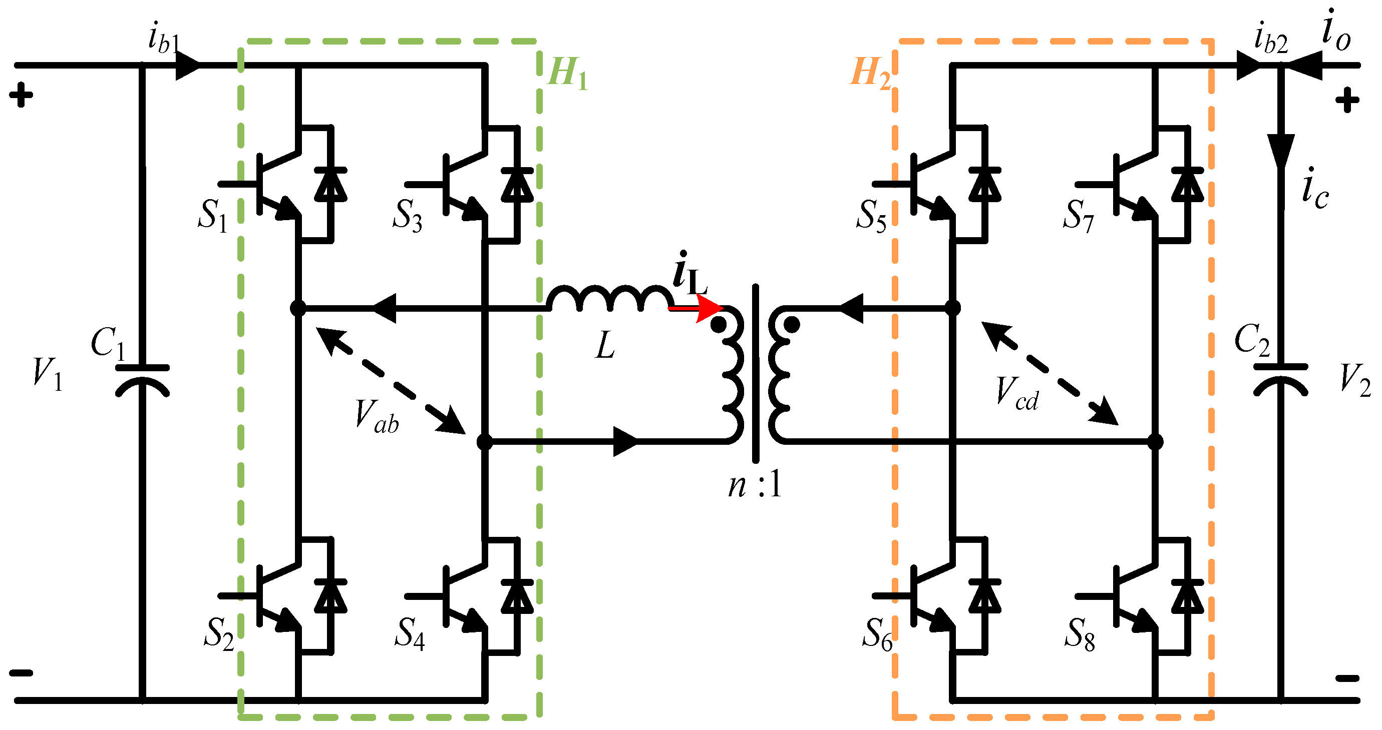
Figure 1 illustrates the DAB converter’s structure, consisting of two symmetrical full-bridges, a coupling inductor L, and a high-frequency transformer (HFT) with a turns ratio n. The HFT provides galvanic isolation, while the inductor L facilitates energy transfer. V1 and V2 denote the DC input and output voltages, respectively, and iL is the current through the inductance.
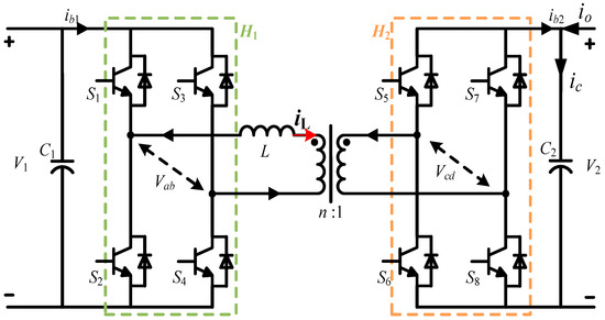
Figure 1.
The topology structure of DAB converter.
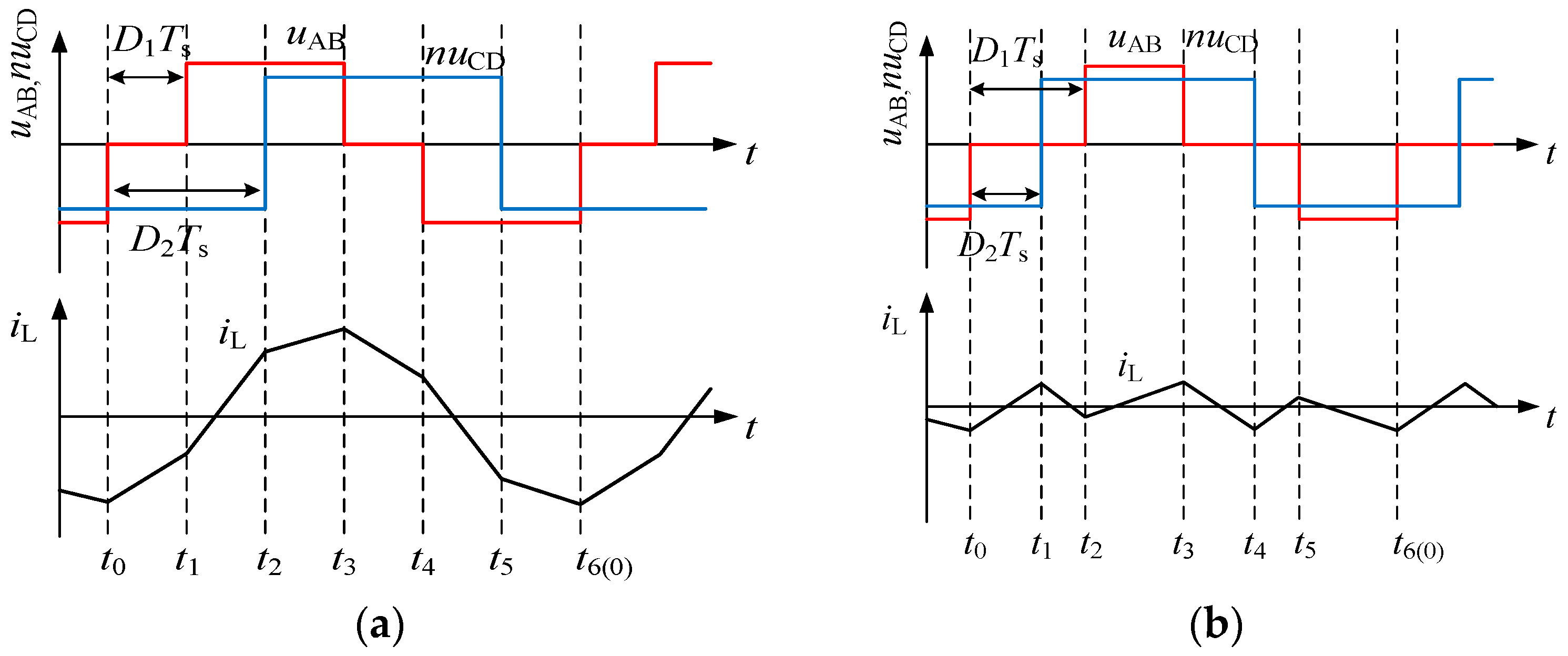
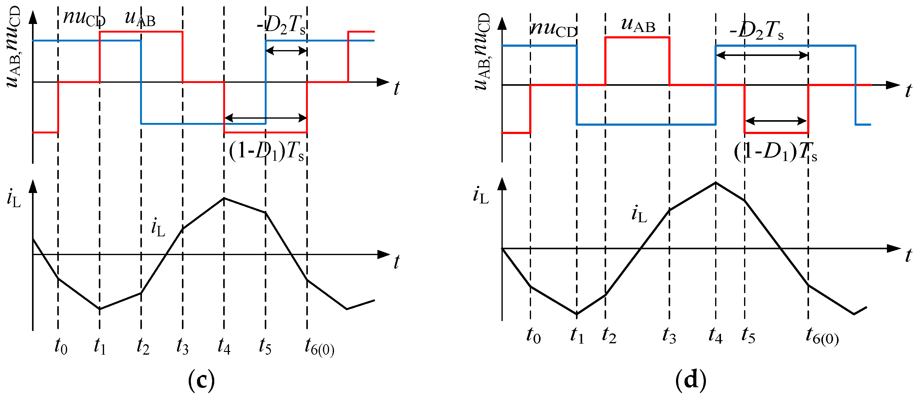
TS is a switching period, fS = 1/(TS) is switching frequency, and D1 and D2 are the inner and outer phase-shift ratios in half a switching period. Under EPS control, the converter can operate in two main working modes depending on the different configurations of the displacement ratio D. D1 is the inner phase-shift ratio between the trigger pulse of S1 and S4. D2 is the outer phase-shift ratio between the trigger pulse of S1 and S5. The conventional operating states of DAB converters under EPS control can be clearly classified into four conditions: one is ; the second is . And considering that DAB can achieve bidirectional power flow, there are four working modes in total: the relationship between the D1 and D2 of the other two conditions, namely, and . The steady-state waveforms of the four modes are shown in Figure 2, including the AC side voltage and inductor current. It can be inferred that the distinct power flow directions characterize the various modes. Maintaining a stable output voltage is challenging due to potential fluctuations. To assess the impact of voltage fluctuations on the output side, the concept of the voltage conversion ratio is utilized, and we define its expression as . When k > 1, DAB operates in boost mode.

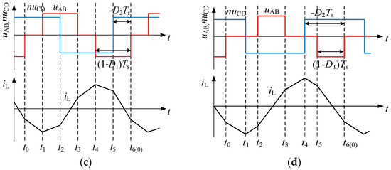
Figure 2.
AC side voltage and inductor current of DAB converters under the EPS control method: (a) mode I, ; (b) mode II, ; (c) mode III, ; (d) mode IV, .
To calculate the inductor current, the circuit of the DAB converter could be simplified into two voltage sources and a series-connected inductor. The inductor current is related to the output voltage of the two H-bridges, as shown below:
Taking the waveform in Figure 2a as an example, we analyze the inductor current. The inductor current is symmetrical within one cycle: . Combining with Formula (1), the expression for the inductor current can be obtained as follows:
According to Formula (2), we can conclude that the different values of the peak currents of the inductor of the DAB converter under the two operating states when and are expressed as follows:
Based on the above analysis, the power transmission of the DAB converter under EPS control can be obtained as follows:
We standardize the output power of EPS modulation, combining with Formula (4). The per unit value of output power can be obtained as follows:
Equation (4) can be rewritten as follows, and PN can be written as (6) and (7):
Using the above analysis method, the peak current and transmission power of the DAB converters of modes II, III, and IV can be derived as in Table 1.

Table 1.
Expression of per unit value for transmission power and current stress.
3. Proposed Current Stress Minimization Algorithm
3.1. Objective Function and Constraint Equations
The PSO algorithm is favored for its light computational load, minimal parameter tuning, and rapid convergence. It is utilized here to develop a method that minimizes current stress, thereby enhancing the efficiency of DAB converters. A crucial aspect of employing the PSO algorithm is setting the objective function and defining the constraints. This paper focuses on minimizing the inductor current stress, as detailed in Table 1. The mathematical formulation of the objective function for reducing current stress is as follows:
The constraint equations based on the working principle of DAB converter can be expressed as follows:
The above constraints include linear constraints and nonlinear constraints. Under normal circumstances, the upper and lower limits of the variables can be adjusted to ensure that the algorithm achieves phase-shift constraints during operation. However, for nonlinear constraints, “”, it is not possible to adopt the transmission power equality constraint equation as the constraint condition for the PSO algorithm directly. Therefore, in order to satisfy the constraint condition, a penalty function is added to the objective function. The objective function and penalty function can be expressed as follows:
where G(D1, D2) represents the fitness function of the current stress. In order to restrict unconstrained optimization problems, penalty functions are introduced to achieve computational solutions that are approaching the true optimal solution. indicates the penalty coefficient, and it is 2000 in this article.
3.2. Algorithm Flowchart
The particle swarm algorithm considers all particles as explorers in the search space, adjusting their flight direction and speed based on their individual best position and group best position and iteratively optimizing in this way. This mechanism based on information sharing between particles constructs an effective group learning environment, promoting the collective evolution of particles towards the global optimal solution. In summary, particles iterate their position and velocity according to the following equation:
where t is the iteration index; C1 and C2 are two positive constants; and are two randomly generated numbers such that , ; is the best solution found by particles in their exploration process, which is the individual extremum; is the optimal solution obtained by the entire particle swarm through collaborative exploration, namely, the global extremum; and is the inertia weight constant used to balance the exploration and utilization ability of particles.
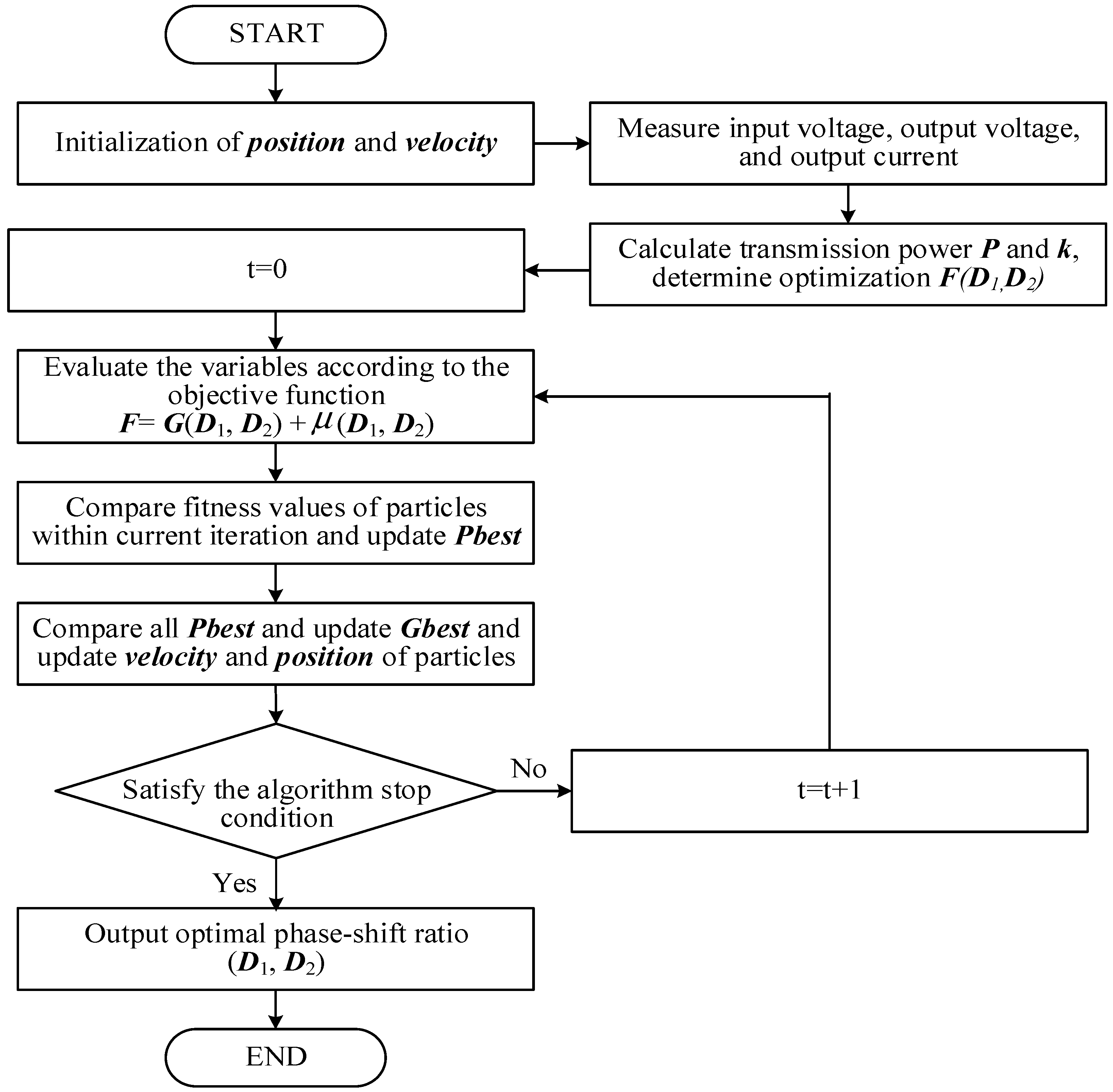
The flowchart of the PSO algorithm is shown in Figure 3. Before executing the iteration, we randomly generate a vector of particle position X (random EPS solution). During the setup phase, the algorithm incorporates the fitness function’s constraints, assigns a random starting position and velocity to each particle, and initializes the iteration count, resulting in the creation of a random particle swarm. At this stage, the individual best position for each particle and the swarm’s global best position are also identified. Then, in each iteration, the particles update their velocity and position based on the current velocity, individual optimal position, and global optimal position. We calculate the fitness function and evaluate individual optimal solutions. By inputting particle position and velocity into the objective function, the algorithm will evaluate fitness performance. After updating, we evaluate the new position of each particle and compare it with its individual best and the global best of the population. If a better position is found, we update and accordingly. Finally, the algorithm checks for the fulfillment of the termination criteria. If the criteria are met, the process is halted; otherwise, the iteration continues.
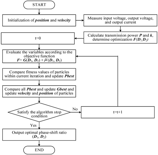
Figure 3.
Flowchart of the proposed optimization.
4. Comprehensive Performance Optimization Control of DAB Converter
Traditional DAB converters use PI control to ensure stable output voltage and improve the dynamic performance of the DAB converter. However, the dynamic response speed of the PI controller is relatively slow, and the adjustment time for input voltage or load sudden changes is long. The transmission power is a function of the phase-shift ratios D1 and D2, where L, f, n, and output voltage can be considered constants. Through analysis, it can be concluded that there is a linear relationship between the output voltage and the output power; therefore, P can be obtained by the DMC algorithm. This paper adopts the dynamic matrix control algorithm (DMC) to improve the dynamic performance of the converter. The DMC algorithm includes three parts: prediction model, rolling optimization, and error feedback.
4.1. Prediction Model
First, it is necessary to obtain the step response of the DAB converter and to take sampling values. From Figure 4, when the DAB converter applies a phase-shift ratio of to the input signal, the response curve of the output voltage Vo is obtained. And a finite set consisting of sampled values of the output voltage step response is used to describe the dynamic characteristics of the DAB converter. The vector is called the model vector, and N is called the modeling time domain.

Figure 4.
Schematic diagram of DAB converter voltage step response curve.
From the proportional and superposition characteristics of linear systems, it can be inferred that by providing an input increment of to the DAB converter at time k, the obtained model vector can predict the future output voltage at time . When there are M consecutive control increments
, ,…, acting on the DAB converter at the moment of k, the predicted output voltage at time is obtained as follows:
where ; is the initial prediction value for at time k.
4.2. Optimize Scrolling
Rolling optimization is an optimization measure based on optimal tracking error and minimum control variation. The optimization performance index at time k can be expressed as follows:
where and are, respectively, the error weight matrix and the control weight matrix; is the output reference value of DAB converter; P is the prediction time domain scale; and M is the control time domain scale;
The control increment is derived from the necessary conditions of the extreme value . The real-time control can be obtained by superimposing the control quantity of the previous moment :
where the control vector is the intermediate variable and is the Toplitz matrix obtained by the model vector parameter , which can be expressed as follows:
According to the principle of homogeneous additivity, the dimensional prediction output matrix can be obtained as follows. At the next time, a similar optimization problem can be proposed to solve , and the future finite time domain can be optimized via rolling optimization.
where is the prediction matrix after rolling optimization; is the initial prediction matrix at time k; and is the control increment.
4.3. Feedback Correction
Due to the inaccuracy of the vector parameters obtained from the DAB converter model, as well as the presence of interference in the system, there may exist errors for the predicted output voltage value and the actual output value. Therefore, it is necessary to correct the predicted voltage value to be closer to the expected output voltage trajectory and achieve closed-loop control. Based on the predicted initial value at the moment of k and the input effect of power increment , the predicted voltage output value at time is obtained as follows:
where is the predicted initial value of the output voltage for N future moments at the moment of k.
DMC can measure the actual output voltage value of the DAB converter at the moment of and compare it with the predicted value , resulting in an error output of the following:
Error values can be used to correct other predicted values at future times:
where .
We introduce displacement matrix S to obtain the predicted initial value for the next moment:
With the predicted initial value for the next moment, optimization calculations can be performed to determine the control increment for k + 1 moment. The entire control process is repeatedly carried out online using a rolling optimization method that combines feedback correction.
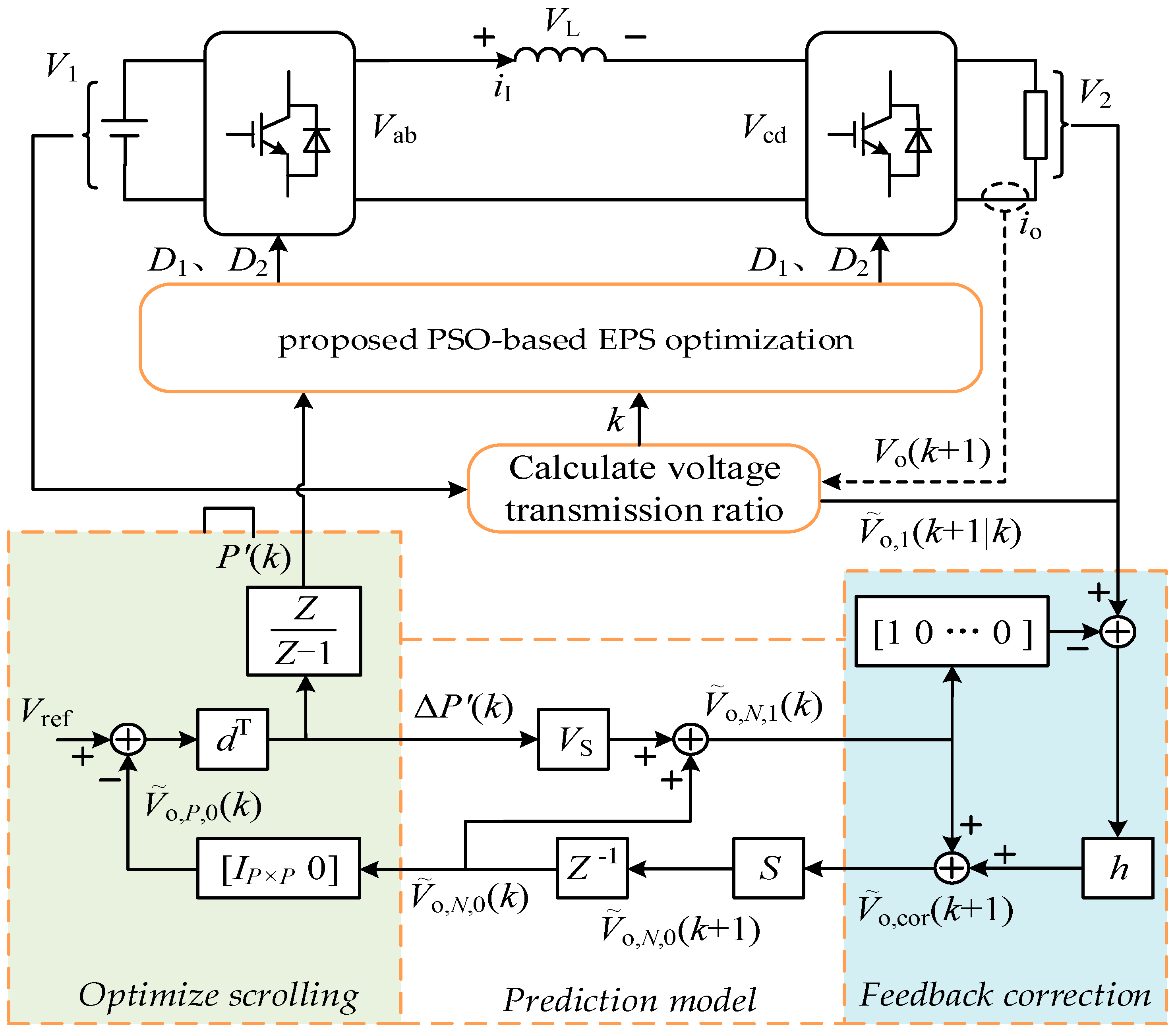
The control block diagram combining DMC voltage prediction control and PSO algorithm is shown in Figure 5. z represents delay.
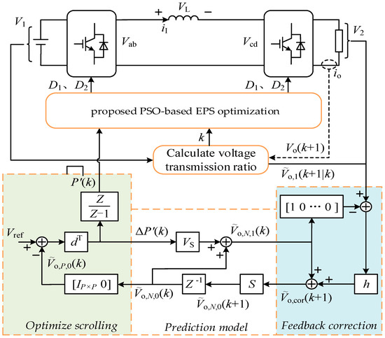
Figure 5.
The control block diagram combining DMC voltage prediction control and PSO algorithm.
5. Analysis of the Results
5.1. Analysis of the Simulation Results
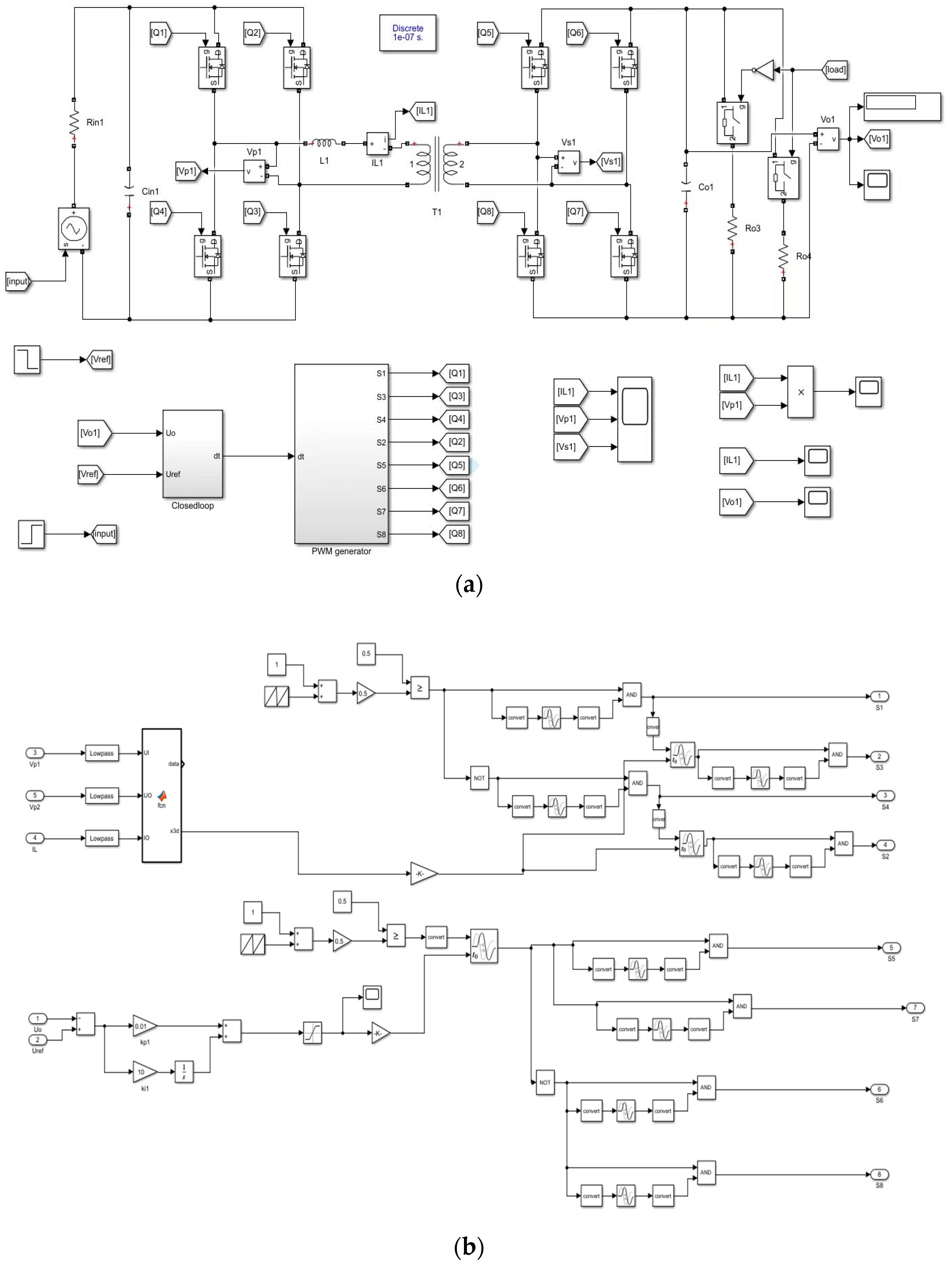
The simulation results of current stress of current iL are presented with the SPS-PI, DPS-PI, EPS-PI, and IDAB-DMC methods for the DAB converter, and the simulation results of the output voltage performances are presented with the initiate reaction, sudden load changes, input voltage, and reference voltage changes with the ESP-PI and IDAB-PSO methods for the DAB converter. The parameters for the converter components and the controllers’ gain are given in Table 2 and Table 3, respectively. DAB converter simulation model diagram and IDAB-DMC control module diagram are shown in Figure 6.

Table 2.
Key parameters of the DAB converter.

Table 3.
Key parameters of the DMC.

Figure 6.
Simulation block diagram: (a) DAB converter simulation model; (b) IDAB-DMC control module.
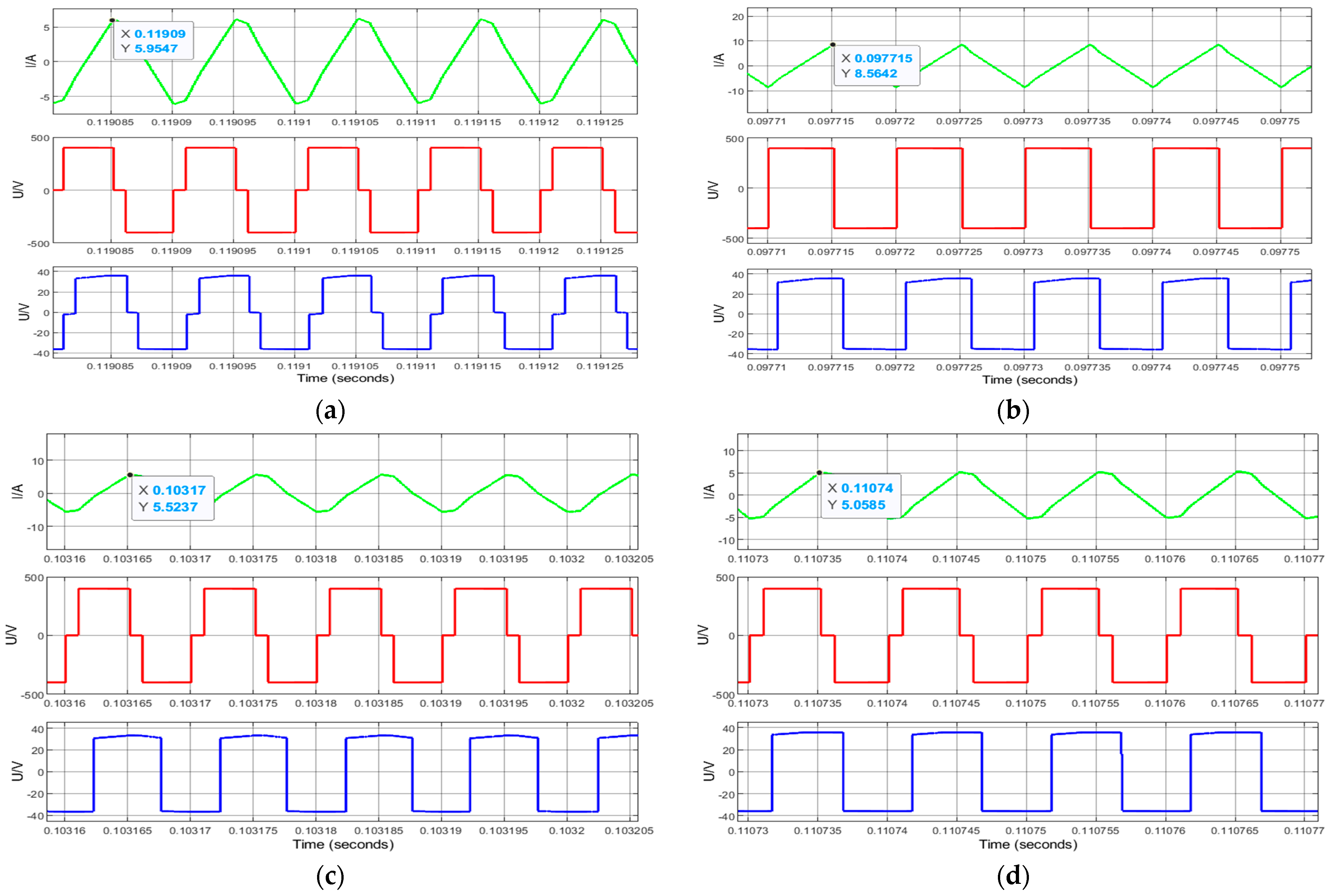
Under the conditions of a simulated input voltage of 400 V, a reference voltage of 36 V, and a load of 7.5 Ω, Figure 7a–d show the current stress waveforms of the converter under traditional SPS, DPS, an EPS control, as well as the optimized control algorithm (IDAB-DMC) combined with the PSO algorithm and the DMC algorithm. The first row represents the current stress, while the second and third rows represent the bridge voltage on both sides.
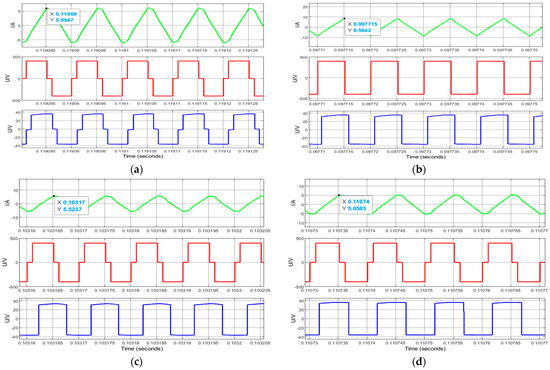
Figure 7.
Current stress under four different controls: (a) DAB current stress under SPS−PI control; (b) DAB current stress under DPS−PI control; (c) DAB current stress under EPS−PI control; (d) DAB current stress under IDAB−DMC control.
From Figure 7, the current stress generated by the converter under SPS-PI control is about 8.56 A. The current stress generated under DPS-PI control and EPS-PI control can be reduced to 5.95 A and 5.52 A, while the optimized current stress after the improved algorithm is 5.05 A. Compared with EPS control, the current stress of the optimized control mode is reduced by 0.47 A. The current stress of the DAB converter is significantly reduced under improved control proposed in this article.
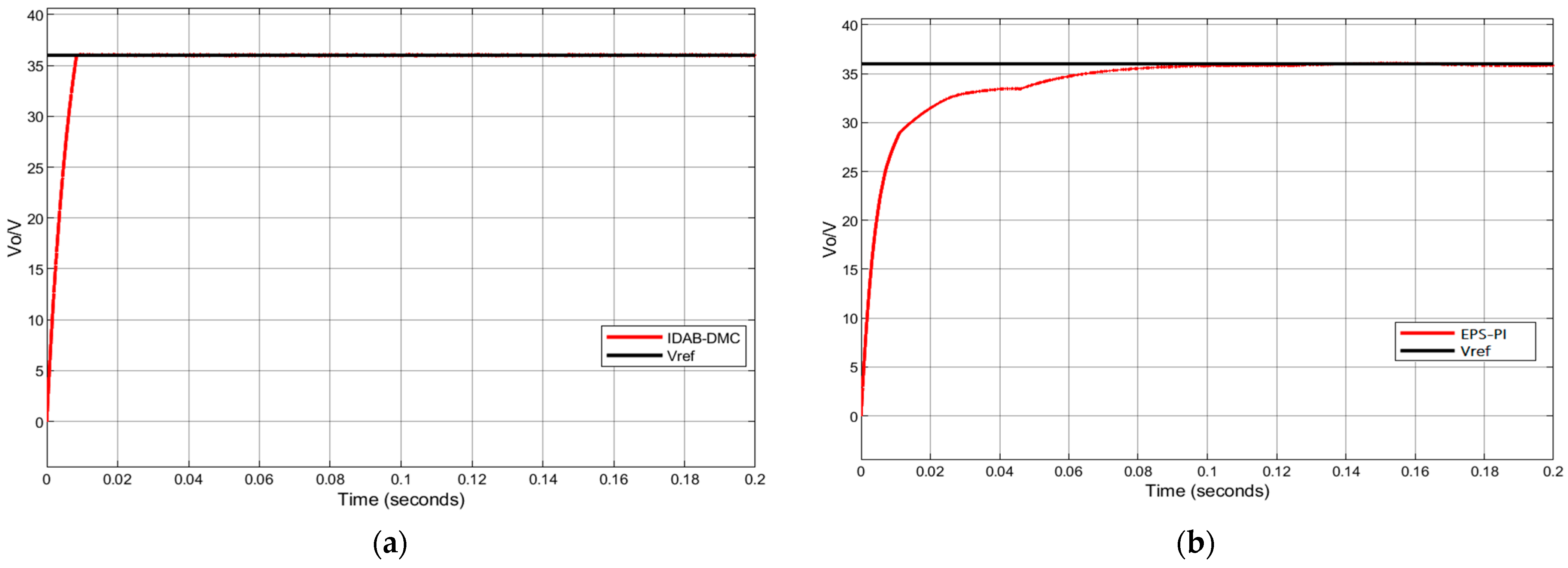
To verify the improvement of dynamic characteristics, the extended phase-shift DAB simulation waveform under traditional PI control and the extended phase-shift DAB simulation waveform under IDAB-DMC control were compared. When the input voltage is 400 V, the reference voltage is 36 V, and the load is 7.5 Ω. Figure 8 shows the starting waveform of the output voltage of the converter under two different controls.
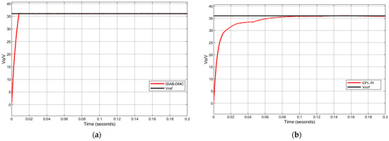
Figure 8.
Starting waveforms under two types of control: (a) starting waveforms under EPS-PI control; (b) starting waveforms under IDAB-DMC control.
From Figure 8, the response time required to stabilize the voltage at 36 V under traditional PI control is 85 ms, while the time required to reach the rated voltage under IDAB-DMC control is 9 ms. Comparing the starting voltage waveforms of two different control methods, it can be seen that the dynamic response speed of the IDAB-DMC controlled converter is improved; the time is 74 ms.
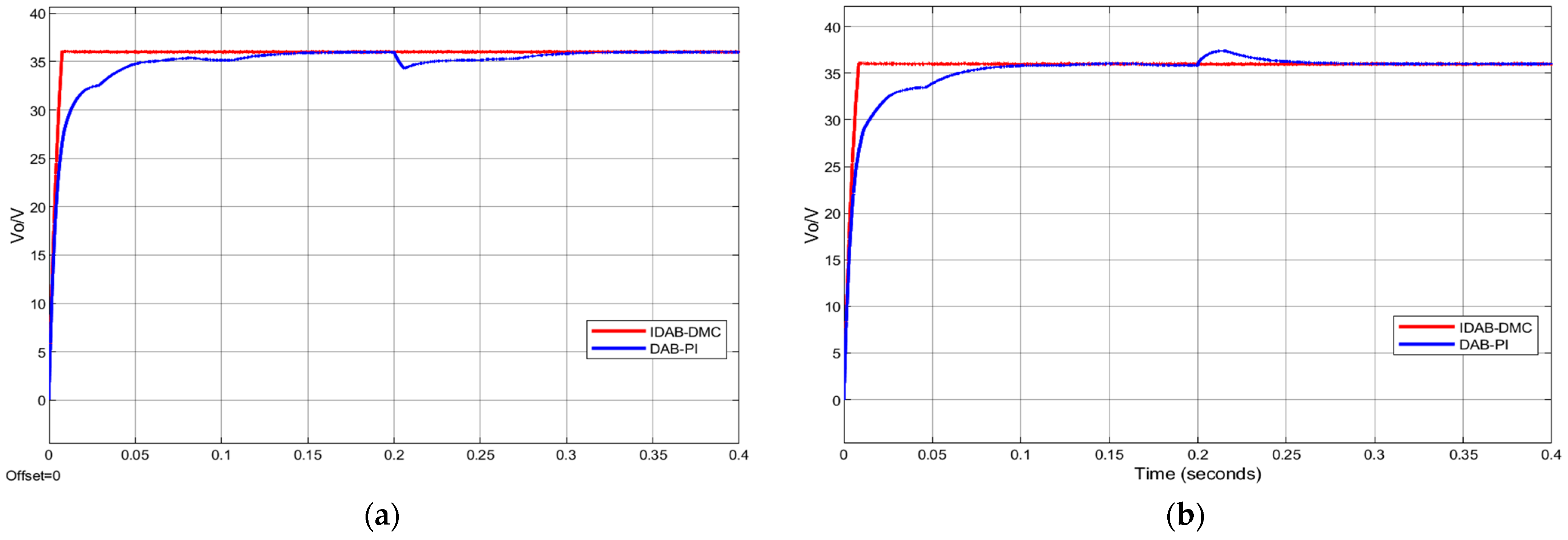
When keeping the input voltage and reference voltage constant and setting the time of load sudden change at 0.2 s, the voltage dynamic curve under different control methods is shown in Figure 5 and Figure 6 when the load suddenly decreases from 7.5 Ω to 7 Ω and suddenly increases from 7.5 Ω to 8 Ω.
From Figure 9, for the adjustment of dynamic performance, both control schemes can stabilize the input voltage back to the reference value. However, under traditional PI control, the voltage fluctuation range of the converter is large, and it takes a short period of time to adjust before returning to the reference value. Under IDAB-DMC control, the converter only needs a few switching cycles to stabilize, with almost no voltage fluctuation.
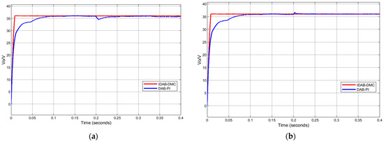
Figure 9.
Comparison of simulated waveforms under two different controls during sudden load changes: (a) simulation waveform of sudden load reduction; (b) simulation waveform of sudden increase in load.
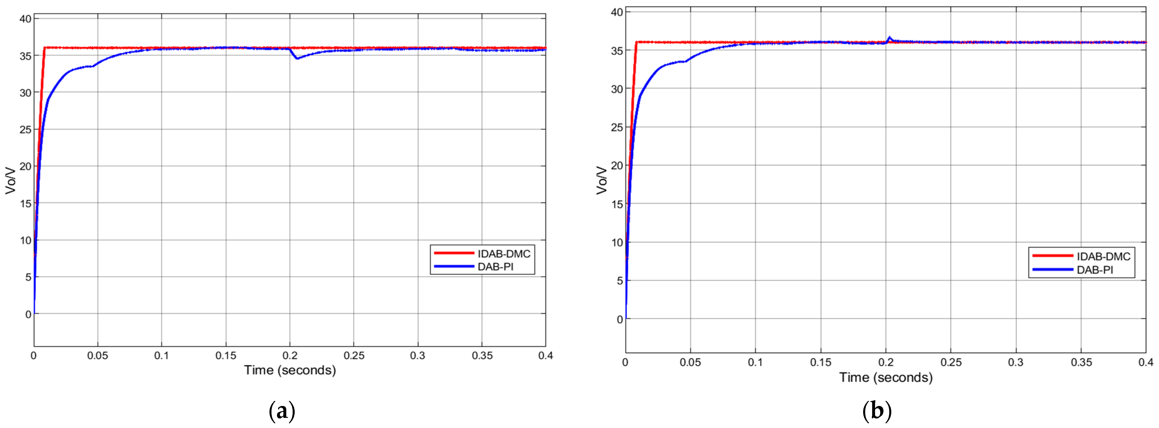
When keeping the load constant and the reference voltage constant, we set the moment of sudden change in input voltage at 0.2 s. For the moment when the input voltage suddenly decreases from 400 V to 350 V and suddenly increases from 400 V to 450 V, the voltage dynamic simulation waveforms under different control methods are shown in Figure 10.
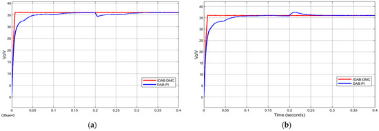
Figure 10.
Comparison of simulated waveforms under two different controls during sudden changes in input voltage: (a) sudden decrease in input voltage; (b) sudden increase in input voltage.
The simulation results when the input voltage suddenly decreases are shown in Figure 10a. Under IDAB-DMC control, the output voltage of the converter hardly fluctuates and remains stable at the reference value; under the traditional PI control strategy, the output voltage of the converter requires a 90 ms adjustment time to recover the steady-state value and has a large fluctuation range. Figure 10b shows the simulated waveform when the input voltage suddenly increases. At this time, the response time of the DAB converter controlled by PI is about 60 ms, while the output voltage fluctuation of the converter controlled by IDAB-DMC is still very small, and the adjustment time is approximately zero.
Similarly, at a sudden change time of 0.2 s, while keeping the input voltage and load constant, the dynamic response waveforms of the reference voltage changing from 36 V to 32 V and 40 V, respectively, are shown in Figure 11.

Figure 11.
Comparison of simulated waveforms under two different controls during a sudden change in reference voltage: (a) sudden decrease in reference voltage; (b) sudden increase in reference voltage.
From Figure 11, we can conclude that when the reference voltage suddenly decreases or increases, the response time of the output voltage following the reference voltage under PI control is 40 ms and 55 ms, respectively. However, IDAB-DMC almost instantaneously follows the given value during the sudden decrease, and it only takes about 5 ms during the sudden increase. The dynamic response time comparison between the two is obvious.
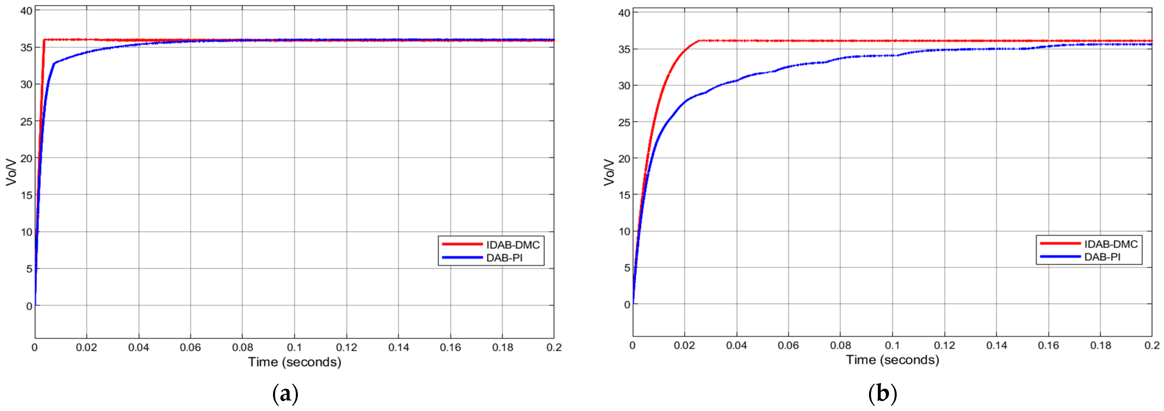
Through the above simulation comparisons, it can be seen that the dynamic performance of the DAB converter is significantly improved under IDAB-DMC control. However, in practice, due to errors in the inductance winding process, wire diameter coils, etc., the actual inductance value may be greater or less than the standard value. Therefore, simulation comparisons were conducted for such situations, and the simulation waveform is shown in Figure 12.
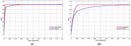
Figure 12.
Dynamic curve when the actual parameters of the inductor do not match the standard: (a) L is greater than the standard value; (b) L is less than the standard value.
From Figure 12, when the actual circuit parameters of the inductance are less than the set value, the steady-state time of both controls decreases, and the output voltage can still follow the reference value. However, when the actual circuit inductance parameters are greater than the set value, the output voltage of the DAB converter controlled by PI cannot follow the reference voltage well, and the start-up time increment is much larger than that of IDAB-DMC control.
5.2. Analysis of the Experimental Results
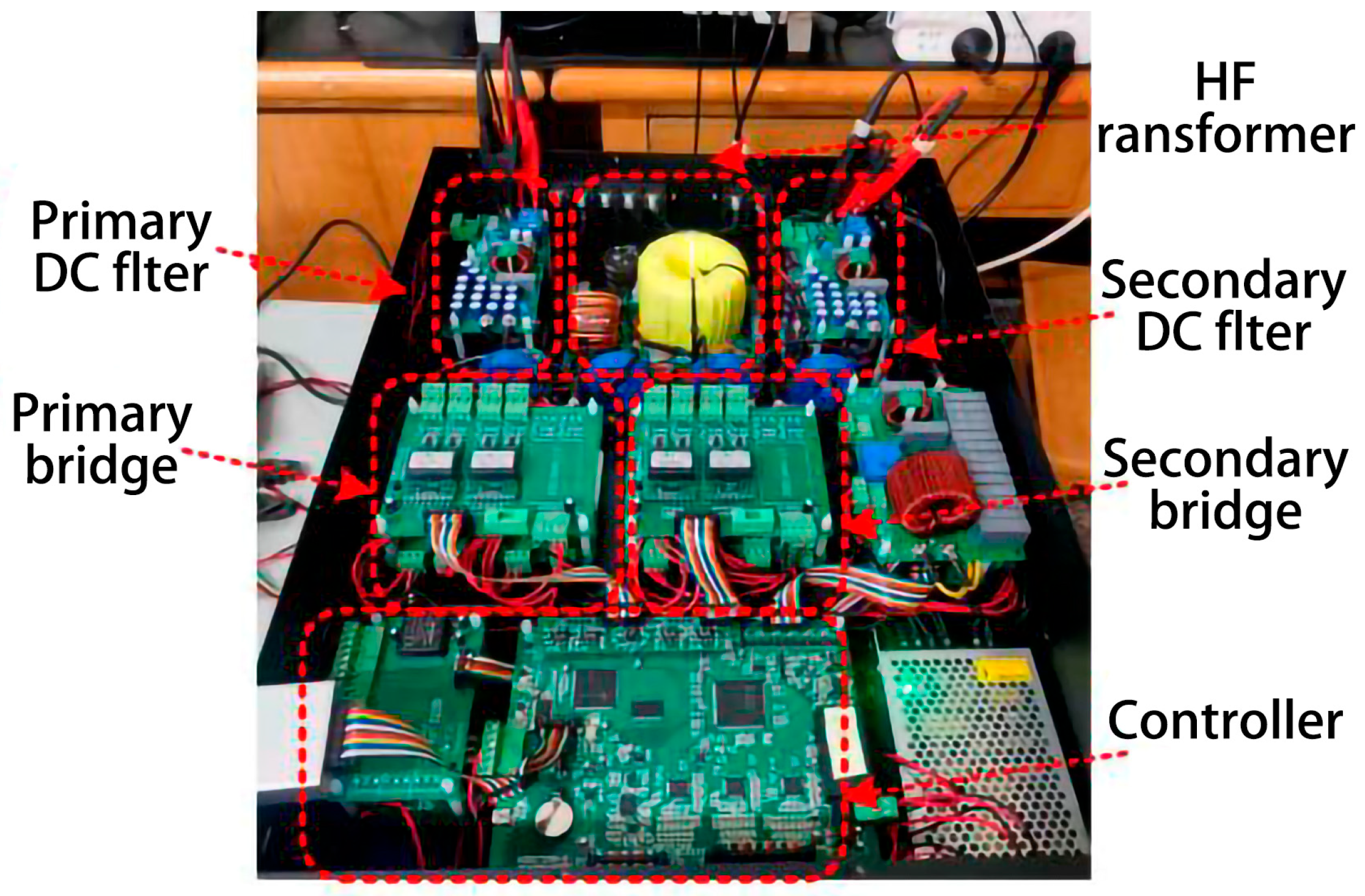
The system parameters of the DAB converter for hardware implementation are given in Table 2. To verify the correctness of the theoretical analysis in this article and the effectiveness of the proposed control strategy, this section combines simulations and uses a DSP model TMS320F28335 (Texas Instruments, Dallas, TX, USA) as the main controller to build an experimental platform, as shown in Figure 13.

Figure 13.
DAB-based prototype.
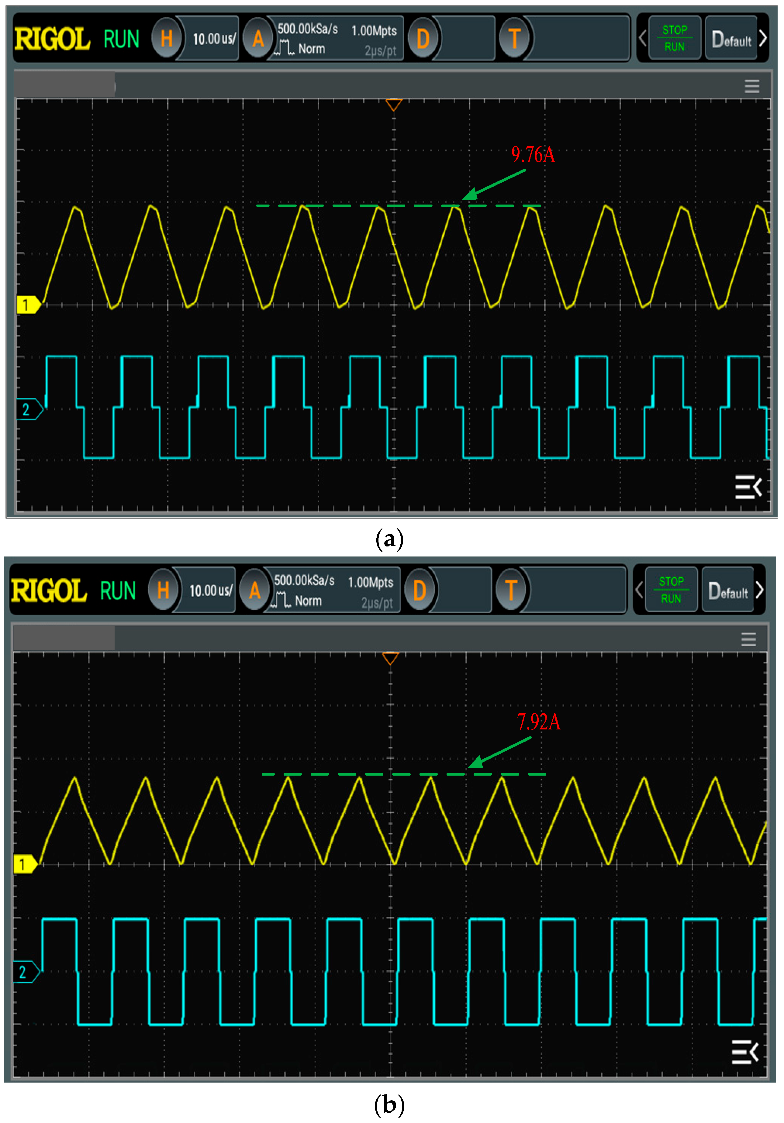
To verify whether the IDAB-DMC control strategy improves performance in actual circuits, comparative experiments were conducted on PI control and IDAB-DMC algorithm control on the established experimental platform. Figure 14a,b show the oscilloscope waveforms of the steady-state current stress of the converter under two different controls.
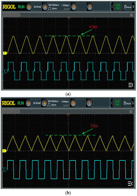
Figure 14.
Current stress waveform diagram under two types of control: (a) current stress under PI control; (b) current stress with IDAB-DMC control.
From Figure 14, it can be seen that the current stress controlled by PI is 9.76 A, while the current stress controlled by IDAB-DMC is reduced to 7.92 A. Therefore, the IDAB-DMC algorithm reduces the current stress, the current stress is reduced by 1.84 A.
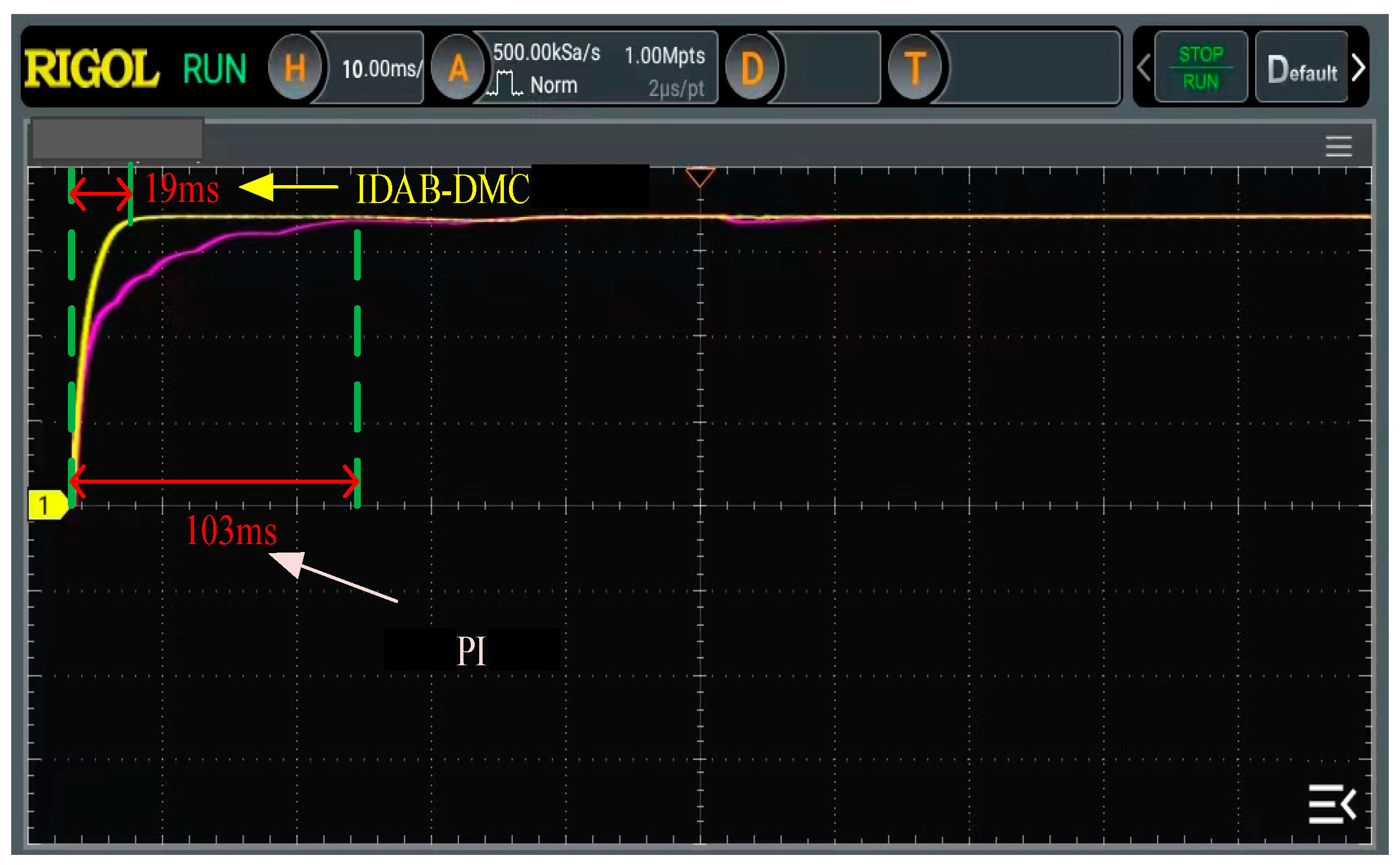
Further comparative experiments were conducted on the dynamic performance of DAB converters under two different controls. First, the startup waveform was compared, as shown in Figure 15.
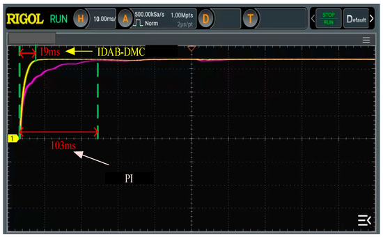
Figure 15.
Comparison of startup voltage waveforms under two different controls.
As shown in Figure 16, the starting time of the DAB converter under traditional PI control is 103 ms, while under IDAB-DMC control, it only takes 19 ms to reach the steady-state output voltage value. The comparison of the starting speed between the two controls is obvious. Therefore, the IDAB-DMC algorithm can significantly improve the startup speed of DAB converters.
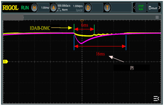
Figure 16.
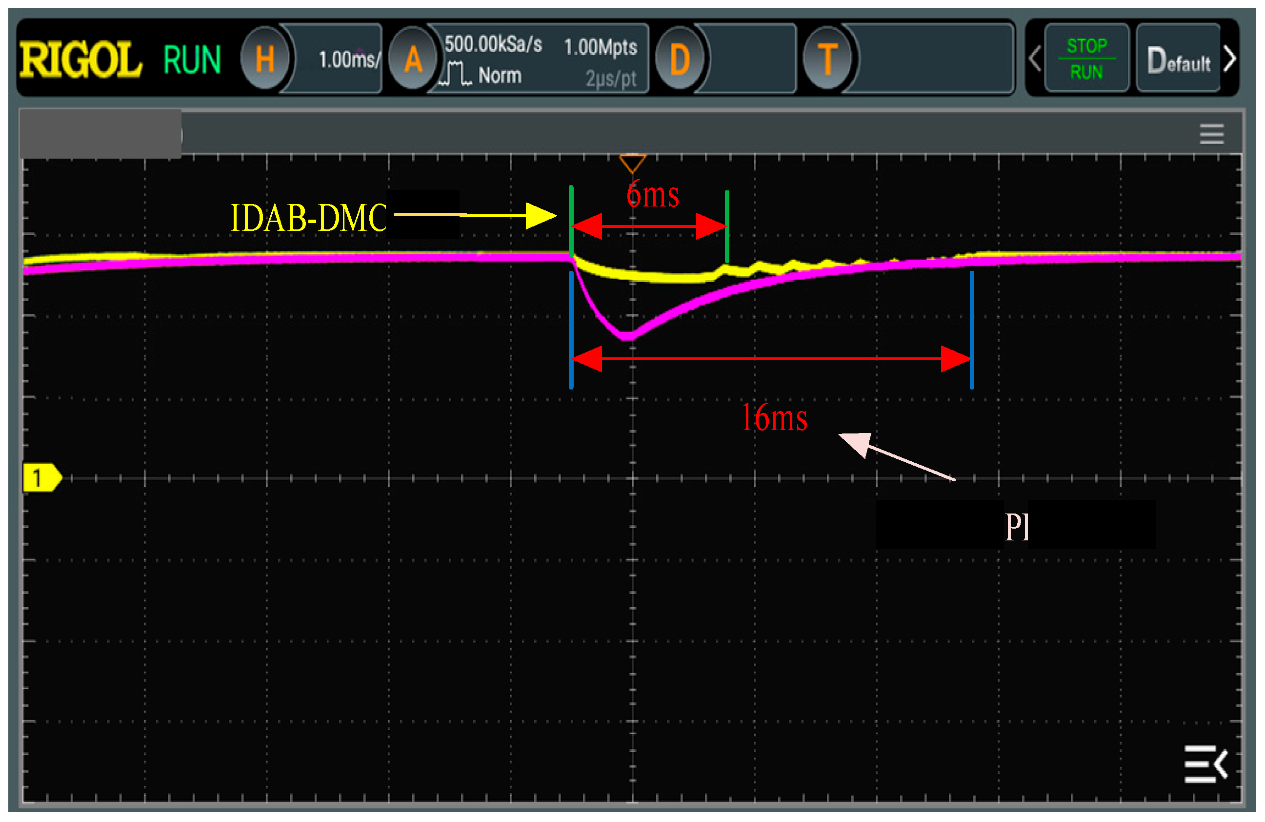
Comparison of two control output voltage waveforms during input voltage disturbance.
Due to external interference in actual operating conditions, there may be disturbances at the input or output terminals. Therefore, sudden changes are applied to the input voltage and load, respectively. Waveform diagrams of the sudden change in the input voltage under both controls are shown in Figure 16, and the waveform diagrams of the sudden change in the load are shown in Figure 17.
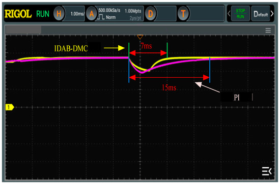
Figure 17.
Comparison of two control output voltage waveforms during load disturbance.
From the experimental waveform, when the input voltage changes, the output voltage of the converter fluctuates greatly under PI control, and it takes 16 ms to restore steady-state conditions. However, under IDAB-DMC control, the voltage oscillates slightly, and the fluctuation time is reduced to 6 ms. When the load is disturbed, the output voltage fluctuates under both controls, but under IDAB-DMC control, the output voltage of the converter can recover to the reference voltage in only 7 ms, while the dynamic response time of the PI controlled converter is 15 ms. Therefore, the IDAB-DMC algorithm improves the dynamic response capability of the DAB converter.
6. Conclusions
This paper introduces an innovative control strategy that integrates particle swarm optimization (PSO) and dynamic matrix control (DMC) algorithms to enhance the performance of a converter. The PSO is employed to alleviate the converter’s current stress, leveraging its optimization capabilities to determine the converter’s displacement ratio. This approach ensures optimal current stress reduction under global conditions, thereby enhancing the system’s steady-state performance. To address dynamic performance, the DMC algorithm is incorporated alongside the PSO, aiming to maintain optimal current stress across the converter’s global range while also bolstering the dynamic response of the DAB converter. Through simulations comparing the IDAB-DMC algorithm-controlled converter with a conventional PI-controlled one, and through subsequent hardware experimental validation, it is demonstrated that the advanced algorithmic control not only reduces converter current stress but also significantly improves the DAB converter’s dynamic performance during system startup, load variations, and input voltage fluctuations. This achieves the objectives of stress reduction and dynamic performance enhancement in DAB converters.
Author Contributions
Conceptualization, D.J.; methodology, D.J.; software, D.J.; validation, D.J., D.W. and D.J.; formal analysis, D.J.; investigation, D.J.; resources, D.W.; data curation, D.J.; writing—original draft preparation, D.J.; writing—review and editing, D.J.; visualization, D.J.; supervision, D.J.; project administration, D.W.; funding acquisition, D.W. All authors have read and agreed to the published version of the manuscript.
Funding
This research received no external funding.
Data Availability Statement
Data are contained within the article.
Conflicts of Interest
The authors declare no conflicts of interest.
References
- Guan, Y.; Cecati, C.; Alonso, J.M.; Zhang, Z. Review of high-frequency high-voltage-conversion-ratio DC-DC converters. IEEE J. Emerg. Sel. Top. Ind. Electron. 2021, 2, 374–389. [Google Scholar] [CrossRef]
- Hou, N.; Li, Y.W. Overview and comparison of modulation and control strategies for a nonresonant single-phase dual-active-bridge DC–DC converter. IEEE Trans. Power Electron. 2020, 35, 3148–3172. [Google Scholar] [CrossRef]
- Hu, Y.; Li, Z.; Zhang, H.; Zhao, C.; Gao, F.; Luo, L.; Luan, K.; Wang, P.; Li, Y. High-frequency-link current stress optimization of cascaded H-bridge-based solid-state transformer with third-order harmonic voltage injection. IEEE J. Emerg. Sel. Top. Power Electron. 2021, 9, 1027–1038. [Google Scholar] [CrossRef]
- Alhurayyis, I.; Elkhateb, A.; Morrow, J. Isolated and non-isolated DC-to-DC converters for medium-voltage DC networks: A review. IEEE J. Emerg. Sel. Top. Power Electron. 2021, 9, 7486–7500. [Google Scholar] [CrossRef]
- Shousha, M.; Prodi, A.; Marten, V.; Milios, J. Design and implementation of assisting converter- based integrated battery management system for electromobility applications. IEEE J. Emerg. Sel. Top. Power Electron. 2018, 6, 825–842. [Google Scholar] [CrossRef]
- Das, D.; Basu, K. Optimal design of a dual-active-bridge DC–DC converter. IEEE Trans. Ind. Electron. 2021, 68, 12034–12045. [Google Scholar] [CrossRef]
- Lin, F.; Zhang, X.; Li, X. Design methodology for symmetric CLLC resonant DC transformer considering voltage conversion ratio, system stability, and efficiency. IEEE Trans. Power Electron. 2021, 36, 10157–10170. [Google Scholar] [CrossRef]
- Dong, D.; Agamy, M.; Bebic, J.Z.; Chen, Q.; Mandrusiak, G. A modular SiC high-frequency solid- state transformer for medium-voltage applications: Design, implementation, and testing. IEEE J. Emerg. Sel. Top. Power Electron. 2019, 7, 768–778. [Google Scholar] [CrossRef]
- Tuluhong, A.; Wang, W.; Li, Y.; Wang, H.; Xu, L. Parasitic parameter extraction and identification method for HFT based on DC–DC converter in EV application. IEEE J. Emerg. Sel. Top. Power Electron. 2022, 10, 4303–4318. [Google Scholar] [CrossRef]
- Zhao, B.; Yu, Q.; Sun, W. Extended-phase-shift control of isolated bidirectional DC–DC converter for power distribution in microgrid. IEEE Trans. Power Electron. 2012, 27, 4667–4680. [Google Scholar] [CrossRef]
- Bai, H.; Mi, C. Eliminate reactive power and increase system efficiency of isolated bidirectional dual-active-bridge DC–DC converters using novel dual-phase-shift control. IEEE Trans. Power Electron. 2008, 23, 2905–2914. [Google Scholar] [CrossRef]
- Mou, D.; Yuan, L.; Luo, Q.; Li, Y.; Liu, C.; Zheng, J.; Zhao, Z. Overview of multi-degree-of-freedom modulation techniques for dual active bridge converter. IEEE Emerg. Sel. Top. Power Electron. 2023, 6, 5724–5737. [Google Scholar] [CrossRef]
- Mou, D.; Dai, Y.; Yuan, L.; Luo, Q.; Wang, H.; Wei, S.; Zhao, Z. Reactive power minimization for modular multi active-bridge converter with whole operating range. IEEE Trans. Power Electron. 2023, 7, 8011–8015. [Google Scholar] [CrossRef]
- Guo, F.; Zhang, J.; Huang, Z.; Huang, W. Simultaneous charging station location-routing problem for electric vehicles: Effect of nonlinear partial charging and battery degradation. Energy 2022, 250, 123724. [Google Scholar] [CrossRef]
- Han, L.; Yang, K.; Ma, T.; Yang, N.; Liu, H.; Guo, L. Battery life constrained real-time energy management strategy for hybrid electric vehicles based on reinforcement learning. Energy 2022, 259, 124986. [Google Scholar] [CrossRef]
- Manzolli, J.A.; Trovao, J.P.F.; Henggeler Antunes, C. Electric bus coordinated charging strategy considering V2G and battery degradation. Energy 2022, 254, 124252. [Google Scholar] [CrossRef]
- Semeraro, C.; Caggiano, M.; Olabi, A.-G.; Dassisti, M. Battery monitoring and prognostics optimization techniques: Challenges and opportunities. Energy 2022, 255, 124538. [Google Scholar] [CrossRef]
- Shi, H.; Wen, H.; Chen, J.; Hu, Y.; Jiang, L.; Chen, G. Minimum reactive-power scheme of dual-active-bridge DC–DC converter with three-level modulated phase-shift control. IEEE Trans. Ind. Appl. 2017, 53, 5573–5586. [Google Scholar] [CrossRef]
- Chiasson, J.N.; Tolbert, L.M.; McKenzie, K.J.; Du, Z. A unified approach to solving the harmonic elimination equations in multilevel converters. IEEE Trans. Power Electron. 2004, 19, 478–490. [Google Scholar] [CrossRef]
- Du, Z.; Tolbert, L.M.; Chiasson, J.N.; Ozpineci, B. Reduced switching-frequency active harmonic elimination for multilevel converters. IEEE Trans. Ind. Electron. 2008, 55, 1761–1770. [Google Scholar]
- Meng, L.; Dragicevic, T.; Vasquez, J.C.; Guerrero, J.M. Tertiary and secondary control levels for efficiency optimization and system damping in droop controlled DC–DC converters. IEEE Trans. Smart Grid 2015, 6, 2615–2626. [Google Scholar] [CrossRef]
- Zhou, H.; He, L.; Lin, Z. Low frequency current ripple suppression for two-stage single-phase inverter based on impedance editing. IEEE Trans. Ind. Electron. 2022, 69, 13417–13427. [Google Scholar] [CrossRef]
- Xiong, F.; Li, J.; Yan, D.; Chen, X. Current stress optimization of dual active bridge converter in two-stage single-phase inverter system with second harmonic current shaping. IEEE Trans. Power Electron. 2022, 37, 2606–2624. [Google Scholar] [CrossRef]
- Tang, Y.; Hu, W.; Cao, D.; Hou, N.; Li, Y.; Chen, Z.; Blaabjerg, F. Artificial intelligence-aided minimum reactive power control for the DAB converter based on harmonic analysis method. IEEE Trans. Power Electron. 2021, 36, 9704–9710. [Google Scholar] [CrossRef]
- Wu, J.; Wen, P.; Sun, X.; Yan, X. Reactive power optimization control for bidirectional dual-tank resonant DC–DC converters for fuel cells systems. IEEE Trans. Power Electron. 2020, 35, 9202–9214. [Google Scholar] [CrossRef]
Disclaimer/Publisher’s Note: The statements, opinions and data contained in all publications are solely those of the individual author(s) and contributor(s) and not of MDPI and/or the editor(s). MDPI and/or the editor(s) disclaim responsibility for any injury to people or property resulting from any ideas, methods, instructions or products referred to in the content. |
© 2024 by the authors. Licensee MDPI, Basel, Switzerland. This article is an open access article distributed under the terms and conditions of the Creative Commons Attribution (CC BY) license (https://creativecommons.org/licenses/by/4.0/).

