Abstract
Generating chaos from originally non-chaotic systems is a promising issue. Indeed, chaos has been successfully applied in many fields to improve system performance. In this work, a Buck converter is chaotified using a combination of the switching piecewise-constant characteristic and of anticontrol of chaos feedback. For electromagnetic compatibility compliance reasons, this feedback control method is able, at the same time, to achieve low spectral emissions and to maintain a small ripple of the output voltage and the inductance current. This new feedback implies a fast and non-linear switching action of the Buck MOSFET on a period of the ramp generator. Thus, it is essential to analyze its thermal performance. This is why we propose an original analysis of the influence of anticontrol of chaos and switching frequency variation on junction temperature: we investigate the correlation between the lifetime of the power electronic switching component and its thermal stress due to the addition of chaos. It appeared that a reduction in the current ripple did not degrade the MOSFET junction thermal performance, despite the fast switching of the MOSFET. Furthermore, a small degradation in the MOSFET lifetime was indicated for chaotic behavior versus periodic behavior. Thus, this leads to the conclusion that using anticontrol of chaos produces a low accumulated fatigue effect on a Buck converter semiconductor.
1. Introduction
Chaos has been extensively studied by a large scientific community, as an interesting complex dynamic phenomenon. First, chaos was analyzed as a phenomenon that can occur naturally through variations in system parameters [1,2]. For example, a Buck converter can exhibit chaotic behavior with variation in the current reference [3,4], the inductance [5] of the converter, the load [6], the voltage reference [7], or a control parameter [8,9].
Recently, chaos has evolved to a new phase of control (i.e., suppression of chaos), utilizing chaos or the generation of chaos from an originally non-chaotic system. The goal of purposefully causing chaos (a shift from order to chaos), also known as chaotification or anticontrol of chaos, has garnered a lot of interest lately because of its enormous potential in unconventional applications, with opportunities to employ entirely novel and different strategies.
Numerous chaotic and nonlinear events have been seen in optical or physical systems [10,11]. From the conventional tendency of comprehending and analyzing chaos to using it, the study of chaotic dynamics has changed, such as in financial time series [12]. Chaos anticontrol has attracted increasing interest for secure data transmission, especially in image cryptography [13,14,15]. In biology and medicine, chaos is exploited in the modeling of certain pathologies, leading to therapeutic solutions, notably for the control of epileptic seizures [16] and the analysis of chaotic diseases via fractional-order models of Diabetes Mellitus, Human Immunodeficiency Virus, Ebola Virus, and Dengue models [17]. In addition, neuronal and genetic models illustrate the role of chaos in neuromorphic behaviors and genetic regulation [18,19].
In the field of electrical systems, ref. [20] proposed an anti-oscillation (control of chaos) scheme for a fractional-order brushless DC motor system. This approach aims to eliminate chaotic oscillations in systems with unknown dynamics and immeasurable states, ensuring stable operation by effectively suppressing chaotic behavior. Similarly, ref. [21] introduced the modified chaos grasshopper algorithm, an advanced optimization approach. This algorithm was applied to improve the performance of techno-economic energy management strategies in microgrids incorporating fuel cells, batteries, and photovoltaic systems. A chaos learning butterfly optimization technique with enhanced extraction of the photovoltaic model parameter was presented in [22]. Following a numerical evaluation of the second-law characteristics of a solar water heater with a dual-twisted tape turbulator, ref. [23] used nonlinear calibration with chaos control to establish a thermal energy prediction model for varying Reynolds numbers and twist pitch values.
Switch-mode power supplies produce electromagnetic interference (EMI) at their switching frequency and harmonic frequencies. This interference significantly complicates achieving electromagnetic compatibility (EMC), especially when employing pulse-width modulation (PWM) techniques. The modulation of the switching frequency, as presented by [24,25], is a technique aimed at reducing spectral emissions. In 1999, Deane further proposed the innovative idea of using chaos to improve electromagnetic compatibility by diminishing spectral peaks [26]. However, the application of the classical chaos anticontrol method to switch-mode power supplies increases the overall magnitude of output voltage ripple, a result corroborated later by [27]. In contrast, refs. [28,29] introduced a chaotified nonlinear feedback approach capable of achieving low spectral emissions, while maintaining minimal output voltage ripple by employing chaotic attractors with small dimensions. More recently, ref. [30] proposed a chaos-based pulse-width modulation technique that leverages a logistic map to distribute the harmonics of a Boost converter, effectively reducing electromagnetic interference. Building on these advancements, ref. [31] introduced a novel radio frequency transmitter that utilizes a chaotic sequence generator to minimize output signal hysteresis and applies a modulation process to reduce spectral emissions. Additionally, ref. [32] studied a high-frequency isolated quasi Z-source photovoltaic grid-connected micro-inverter employing chaotic frequency modulation technology to effectively suppress inverter spectral emissions.
The anticontrol of chaos feedback necessitates rapid switching actions in converters, which impose thermal stress on power-switching semiconductor devices [33]. Consequently, it becomes critical to analyze their thermal performance to ensure operational safety and prevent failures of power devices [34]. To evaluate the efficiency and reliability of power electronic systems, semiconductor devices are often modeled as ideal switches in fast simulations, as seen in [35]. However, this approach makes it challenging to accurately calculate Metal Oxide Semiconductor Field Effect Transistor (MOSFET) power losses. Establishing an electro-thermal model [36] is essential to account for the impact of junction temperature on the device parameters.
Numerous electro-thermal models have been presented in the scientific literature. For approximating Insulated Gate Bipolar Transistor (IGBT) switching and on-state losses, Ref. [37] employed the lookup table method. Using inputs such as junction temperature and electrical load, a complete and comprehensive electro-thermal model was proposed by [38]. Similarly, the model by [39] incorporates the interactions between junction temperature and the transistor’s voltages and currents. In [40], power losses were averaged across each switching cycle using a high-speed electro-thermal model. Furthermore, Refs. [41,42] developed a realistic converter model, with parameters derived from component datasheets, the printed circuit board layout, as well as cable length and diameter.
To analyze MOSFET thermal behavior, the most prevalent heat transfer model uses several Foster [43,44] networks. In [45], Nayak and Pramanick utilized a third-order Foster circuit to accurately fit the MOSFET impedance curve provided in the datasheet. Additionally, Ref. [46] proposed various electro-thermal Foster circuit variants to simulate the performance of an electric vehicle inverter.
Changes in the power device junction temperature affect their reliability and lifetime, according to [47]. The Coffin–Manson law is one of the most widely used models for evaluating failure cycles and estimating the lifetime of switching devices. Inverter lifetime [48] is commonly assessed using the rainflow counting algorithm, which takes as inputs the mean junction temperature and the variation in junction temperature [49,50,51]. In [52], an analysis was presented on the influence of chaos on junction temperature, revealing that a chaotic current behavior reduced the MOSFET’s lifetime by half, compared to a periodic current behavior.
MOSFET on-state resistance is not only junction-temperature-dependent but also a failure precursor indicator. Indeed, an increase in increases the MOSFET degradation. The continued modification of imposes an online monitoring for prognosis, in order to evaluate the device lifetime. Indirect temperature measurement methods investigate the relationship between typical thermal-dependent parameters and MOSFET on-state drain-source resistance. The junction temperature is estimated by measuring temperature-sensitive electrical parameters, such as the on-state drain-source voltage [53] and current, the threshold voltage, peak gate current [54], turn-on collector current transient [55], plateau voltage, turn-off collector-emitter voltage transient [56], voltage across source/emitter parasitic inductances [57], turn-on [58], and turn-off [59] delay times. Furthermore, the use of temperature-sensitive electrical-parameter-based sensors increases the overall circuit complexity.
Compared to many studies in the literature, where anomaly monitoring was conducted entirely through simulation, [60] proposed the Processor-in-the-Loop test: an innovative aging monitoring technique, linked to modification, based on the creation of a virtual dataset representative of the aging phenomenon. The design of an estimator of the was based on Artificial Neural Network regression (a simple and compact IA-based model). A more accurate real-time model was developed, including the on-line modifying of . The model predictive control [61] design by the same authors is robust to variations in system parameters, such as load or temperature, incorporating these variations into the optimization problem.
After the chaotification of a Buck converter (in order to reduce spectral emission), the purpose of this article is to analyze the influence of the anticontrol of a chaos controller on the junction temperature and to compare it with a standard feedback (Proportional-Integral PI controller). The anticontrol of chaos feedback (a combination of anticontrol of chaos and a PI standard controller) is capable of simultaneously achieving low spectral emissions, while maintaining minimal ripple for both the output voltage and the inductor current. The results confirm the effectiveness of the chaos anticontrol feedback for achieving low spectral emissions. The quantitative information confirmed that the output voltage power spectrum is reduced by almost half if a chaotified nonlinear feedback is introduced, compared to non-chaotified types. Fast and non-linear MOSFET switchings cause thermal stress. In this study, we propose investigating the correlation between the lifetime of a C2M0080120D MOSFET [62] and its thermal stress due to the anticontrol of chaos and switching frequency variation. A reduction in the current ripple enhances the MOSFET junction thermal performance. A step-by-step process establishes an electro-thermal model of the MOSFET, integrating power losses (which include the conduction, switching, diode conduction, and reverse recovery losses). Finally, the Miner’s model accumulated stress of the MOSFET is quantified, evaluating the number of failure cycles using the Coffin–Manson equation and the thermal cycle number using the rainflow counting algorithm. The accumulated fatigue showed a slight degradation in the MOSFET lifetime with anticontrol of chaos feedback (in comparison to a standard controller), despite the fast switching of the MOSFET. Thus, this leads to the conclusion that using anticontrol of chaos produced a slight degradation in the remaining life of the Buck converter semiconductor.
The main sections of this paper are as follows: Section 2 describes the behavior of a Buck converter with both a standard and anticontrol of chaos controller. In Section 3, the MOSFET power loss calculations and thermal model are detailed. Then, in Section 4, the lifetime model for estimating the damage on a MOSFET is presented. The paper concludes in Section 5.
2. Nonlinear Behavior of a Buck Converter
In this paper, our study is focused on a Buck converter, whose topology is shown in Figure 1. The circuit consists of an inductance L, a diode D, a MOSFET switch (C2M0080120D), a capacitance C, and a load R. The output voltage tracks the reference signal , ensuring the desired stabilized output voltage.
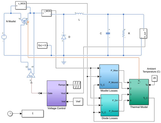
Figure 1.
The Buck converter operates with feedback control.
When the MOSFET is in on-state, the energy is stored in the inductance L and in the capacitance C, and no current flows through the diode D. When the MOSFET is in off-state, the diode now conducts, ensuring a path for the inductor current . The Buck converter uses a periodic switching to step down the input voltage . This is achieved by controlling the power MOSFET using a pulse-width modulated signal. This signal is generated using an error amplifier (i.e., the deviation between the output voltage and a reference voltage), a proportional integral derivative (PID) controller, and the ramp input voltage (characterized by and ) to adjust the duty cycle of the switch. Table 1 summarizes the main specifications of this application.

Table 1.
The main specifications of a Buck converter operated with feedback control.
Despite the continuous advances in control theory, the PID controller is still the most popular control technique employed in feedback control for regulating the output voltage of Buck converters. The standard structure of the controller is as follows:
where P, I, D, and N are the proportional, the integral, the derivative, and the filter coefficients. The parameters of the converter are selected to achieve the desired output voltage.
The inductance current and the MOSFET current of this circuit are generally periodic at the switching frequency (f = 10 kHz), as shown in Figure 2. The simulations were performed with the SimScape toolbox of MATLAB R2020b Simulink and included the buck converter with its control strategy, the power losses, and thermal model. and MOSFET current increased from 15.25 A to 16.75 A when the MOSFET was in on-state. Consequently, the MOSFET mean current was 16 A, with a ripple of 1.5 A. If the MOSFET was in off-state, decreased, meanwhile the MOSFET current was zero.
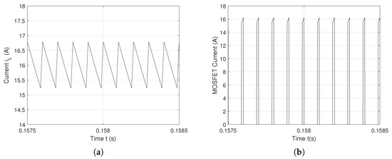
Figure 2.
Plots of (a) and (b) MOSFET current with a stable period-1T operation (f = 10 kHz).
Figure 3a shows the periodic output voltage with a 2.5 V ripple. Its spectrum, shown in Figure 3b, corresponds to the converter governed by the control law of Equation (2). The spectrum consists solely of the fundamental frequency, characterized by a sharp peak at , with a magnitude of −25 dB, and its harmonics.
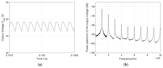
Figure 3.
(a) Output voltage with a periodic behavior (f = 10 kHz); (b) Power spectrum of .
Now, let us introduce the controller with the following control law:
Starting from a regular (non-chaotic) system = , numerous works have been reported on generating continuous time chaotic motion.
- The nonlinear feedback method [13] introduces a nonlinear perturbation = + ·, where is a small control gain and is a nonlinear function which introduce chaos. Feedback methods include the nonlinear time delay feedback control method [63], the linear time delay feedback method, and piece-wise linear function feedback.
- The chaotic coupling [64] of a stable system = with a chaotic system = influences x through the coupling function , which introduces chaos. The new system is = + .
- Bifurcation parameter tuning introduces a bifurcation parameter into a system = and pushes it into the chaotic region with a small variation = + .
- A chaotic impulse can destabilize a stable system with discrete spikes = + ·, where is a Dirac impulse and a chaotic input.
- The noise-introduced chaos [22] system = + adding randomness (e.g., stochastic noise).
In our case, the nonlinear feedback h(x) is a sine function. This time, the controller (3) includes, in addition to PID, a nonlinear feedback controller, with a multiplication of the feedback, introducing the chaos voluntarily. The amplitude and frequency of the resulting control signal dictate the number of switching cycles of the MOSFET. The ramp voltage operates at a constant frequency, while the modulating signals vary (due to the sine), allowing different duty cycles within the ramp period, involving fast switching. Figure 4 shows the ramp wave and the chaos anticontrol feedback, implying controller switching (3). Figure 5 presents the simulation results for inductance current and the MOSFET current obtained with the controller (3). and the MOSFET currents varied irregularly between 15.6 A and 16.4 A. Consequently, the MOSFET mean current was 16 A, with a very small ripple of 0.8 A. The MOSFET switched much more frequently that in the previous case (when the converter operated under the control law of Equation (2)), but no longer periodically. This allowed maintaining a small ripple for the output voltage .
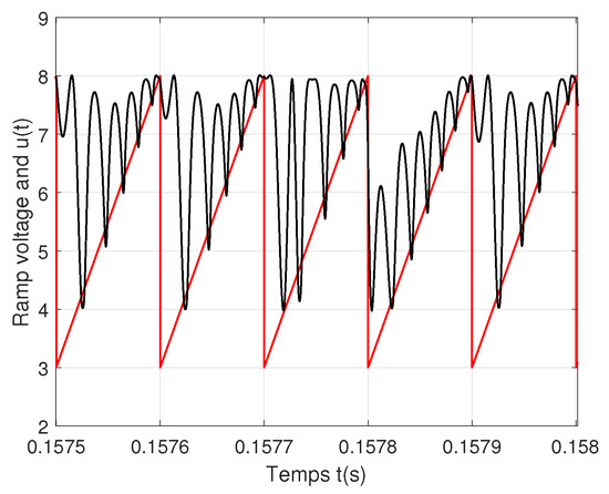
Figure 4.
Ramp wave and chaos anticontrol feedback .
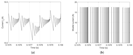
Figure 5.
Plots of (a) and (b) MOSFET current with a chaotic behavior (f = 10 kHz).
The output voltage is now chaotic, with a 1.8 V ripple, as shown in Figure 6a. Therefore, the influence of the controller (3) on the ripple is not negligible. Figure 6b represents the power spectrum of with a peak of −46 dB magnitude at the switching frequency .
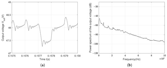
Figure 6.
(a) Output voltage with chaotic behavior (f = 10 kHz); (b) power spectrum of .
The various frequencies in stem from its highly irregular waveform, caused by the intrinsic nonlinear dynamics. These dynamics are driven by the varying on and off durations of the MOSFET switch within each ramp period T. Generally, the power spectrum represents the frequency components at a height given by the peak amplitude of at different frequencies. The link between the ripple and power spectrum magnitude explains the decrease in the peak magnitude from −25 dB to −49 dB. Therefore, the anticontrol of chaos improved the spectral emissions by further reducing the spectral peaks. We observed that the spectrum was no longer composed of a single peak at the switching frequency (or its harmonics). Instead, numerous spectral lines appeared, with a continuous power spectrum characteristic of chaos. Naturally, the reduction in the maximum of the power spectrum was achieved with the presence of chaos, increasing the converter’s switching frequency. As a result, the output voltage exhibited improved frequency-domain (spectral) and time-domain (ripple) performance compared to the first case.
Figure 7 and Figure 8 show the periodic and chaotic output voltages with f = 20 kHz. The influence of the control law (3) and the switching frequency f reduced the ripple of by more than 96%, from 0.8 V to 0.025 V. The chaotification of the feedback decreased the power spectrum of to −79 dB, comparable with the −40 dB with a periodic behavior. A further increase in switching frequency at f = 50 kHz led to the same trend: the ripple was 0.15 V with a periodic behavior and 7.5 mV with a chaotic behavior. The maximum of the power spectrum was reduced from −60 dB to −98 dB, as shown in Figure 9 and Figure 10.
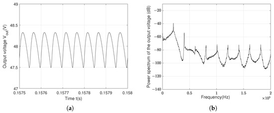
Figure 7.
(a) Output voltage with a periodic behavior (f = 20 kHz); (b) power spectrum of .
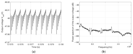
Figure 8.
(a) Output voltage with a chaotic behavior (f = 20 kHz); (b) power spectrum of .
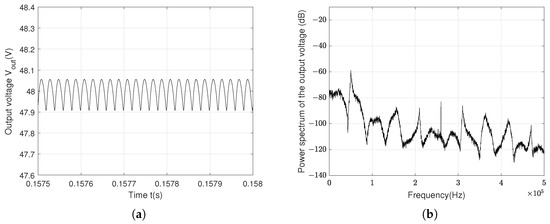
Figure 9.
(a) Output voltage with a periodic behavior (f = 50 kHz); (b) power spectrum of .
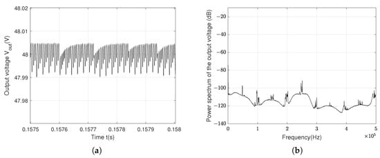
Figure 10.
(a) Output voltage with a chaotic behavior (f = 50 kHz); (b) power spectrum of .
Table 2 summarizes the ripple and power spectrum of the output voltage, using the control laws of Equations (2) and (3) as feedback. The control law of Equation (2) led to a large ripple. Chaotifying the converter with the proposed control law of Equation (3) as feedback ensured a good ripple and caused a spectacular decrease in the power spectrum amplitude. Finally, Table 2 shows that the power contained in the peak harmonics of the output voltage decreased at different frequencies, f = 10 kHz, 20 kHz, and 50 kHz.
Table 2.
Ripple and maximum of power spectrum results for the study cases.
3. Power Loss Computation and Thermal Model
The conduction and switching losses of the MOSFET added to the power losses of the diode are the total power losses, as shown in Figure 1.
3.1. MOSFET and Diode Power Loss Computation
The MOSFET’s conduction power loss () is calculated as the product of the drain-source current flowing through the MOSFET during conduction and the drain-source voltage across it at each time step, as , where depends on the drain-source current and the junction temperature . In order to reproduce this characteristic –, the Shichman–Hodges model describes the off, linear, and saturation regions of the MOSFET using three distinct equations given below:
where is the threshold voltage, is the gate-source voltage, k is the transistor gain, and is the channel length modulation. The drain current of a MOSFET as a function of , , and depends on the MOSFET’s operation region and temperature. The fittype and fit MATLAB functions were used to identify the voltage at two different junction temperatures, 25 °C and 150 °C using the current–voltage characteristics –. Based on Figure 11a, the following polynomial fitting function was obtained:
where a = 2.44 ×, b = −0.001024, c = 0.09757, d = −0.1043 for 25°C; and a = 6.636 × , b = −0.002202, c = 0.1729, d = −0.0759 for 150 °C. The values of the coefficients a, b, c, and d were calculated taking into account the effect of , and of temperature. The lookup table method was utilized to approximate both conduction and switching losses for the MOSFET and diode. A 2-D lookup table using junction temperature and drain-source current as breakpoint inputs interpolates the drain-source voltage for any given and values, based on Equation (5). Then, the conduction power loss is the product of and . During a transition, a refined model of switching loss energy includes the gate drive effect and parasitic capacitances:
where and are the rise and fall times, (depending on ) is the total gate and is Miller charges (depending mostly on and ), and is the gate drive current. A higher , the ratio between the gate-source voltage and gate resistance, reduces switching losses. The gate resistance ( includes internal and external resistance) affects switching losses by influencing the speed of the gate voltage transition. A larger causes slower switching, leading to increased power dissipation in the MOSFET rather than the gate resistor. Since switching losses occur during transitions, increasing increases the transition times and, therefore, switching losses. The impact of junction temperature on switching losses can be approximated by
where is the temperature coefficient of the switching losses. Thus, slower transitions and a higher resistance and junction temperature increase . The C2M0080120D datasheet provides the dependence of switching energy losses on temperature (showing significant variation in junction temperature at a drain-source current of 20 A and a drain-source voltage of 800 V), current (exhibiting substantial variation in drain-source current), and voltage (for drain-source voltage values of 600 V and 800 V). The lookup table interpolates these known values to estimate the switching energy losses at different data points.
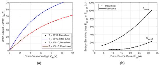
Figure 11.
(a) Fitting curves of the static current–voltage characteristics – at 25 °C and 150 °C; (b) MOSFET energy power losses as a function of the drain-source current , with = 800 V.
Figure 11b presents the switching loss energy when the device turns-on and when the device turns-off. The fitting function for the datasheet points, as represented in the figure, is as follows:
where e = 0.6553, f = 8.452, and g = 75.04 for the on-state of the MOSFET; and e = 0.4597, f = −9.768, and g = 72.87 for the off-state of the MOSFET. The values of the coefficients were calculated taking into account the effect of the junction temperature, and of . Unfortunately, most datasheets only show typical values, at two different temperatures (25 °C and 150 °C), for the current–voltage characteristics –, the switching loss energies and , and the diode characteristic –. Since the characteristics have a strong temperature, voltage, and current dependence, measuring them under actual use conditions is necessary. The lookup table interpolates these known values in order to generate the switching energy losses at different data points.
The switching loss energies when the MOSFET turns on or off depend on , and . Based on Equation (8), a 3-D lookup table having , , and as inputs interpolates at any , , and . Then, the loss energies are used to estimate switching power losses as the product of the loss energies and the switching frequency.
The conduction power loss of a diode is analogous to that of a MOSFET, calculated as the product of the forward saturation voltage and the forward saturation current : , where . Figure 12 presents a comparison between the datasheet points of the diode characteristic and the fitted curve, achieved with the following polynomial fitting function:
where h = 0.4481, i = −1.187, j = −0.1057, and k = 0.6399 for 25 °C, and h = 0.3296, i = 0.708, j = −4.211, and k = 2.078 for 150 °C. In order to estimate the conduction power loss , a 2-D lookup table interpolates the forward saturation voltage (the output of 2-D lookup table) for any forward saturation current and junction temperature values (the breakpoint inputs of 2-D lookup table).
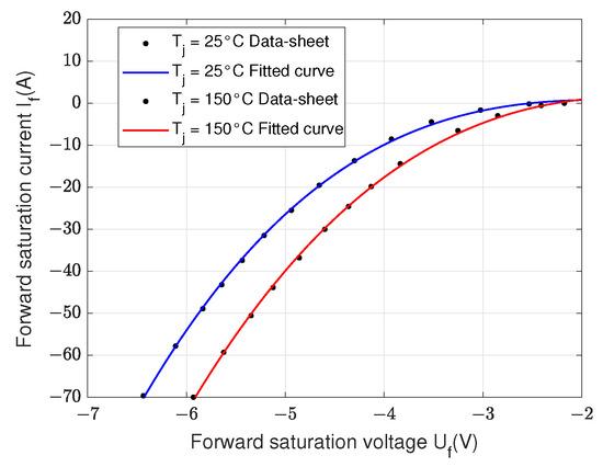
Figure 12.
Diode characteristics at = 25 °C and = 150 °C.
The diode contributes to the switching energy due to the reverse recovery charge during the turning off of the MOSFET. In [36], the following relation is used for :
where is the peak reserve recovery current, S is the snappiness factor, and is the turn-off switching rate. The snappiness factor S is 4.928, calculated from the datasheet information as (25 °C) = 152 nC and / = 1950 A/s. In order to calculate the reverse recovery charge at = 125 °C, /dt is 1090 A/s as in [36], resulting in a value of 271.93 nC. depends on , as follows:
A 3-D lookup table, using , the forward saturation current , and the forward saturation voltage as breakpoint inputs, calculates through interpolation (as the product of and the diode forward saturation voltage ). The diode’s switching power loss, , is then determined as the product of the loss energies and the switching frequency f.
3.2. Thermal Model
The MOSFET junction temperature is estimated using a linear model given by , where is the thermal impedance, is the ambient temperature and represents the total power loss, which is the sum of all power losses (, , and ). The thermal impedance is graphically provided in the datasheet of SiC C2M0080120D MOSFET (Figure 13a). By implementing curve-fitting identification of , the Foster thermal network (a resistor and capacitor thermal network as shown in Figure 13b) is derived. The parameters of the Foster model are = 0.2525 K/W, = 0.18024 K/W, = 0.0342 K/W, = 0.1976 K/W, = 0.42068 Ws/K, = 0.05191 Ws/K, = 0.001285 Ws/K, and = 0.006952 Ws/K. The total power losses are processed through the Foster network, resulting in the junction temperature .
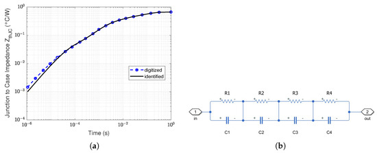
Figure 13.
(a) Comparison between the transient thermal impedance curves obtained through simulation and those provided in the datasheet; (b) Simulink model of the Foster network.
Figure 14a illustrates a stable 1T limit cycle for the junction temperature using the control laws of Equation (2) as feedback with a switching frequency f = 10 kHz. has a periodic waveform with variations from 64.9 °C to 65.11 °C. Therefore, the mean junction temperature was near to = 65.005 °C, and the junction temperature variation was = 0.21 °C. Anticontrol of the chaos controller (3) forced a chaotic behavior for the junction temperature , as in Figure 14b. The mean junction temperature was near to = 65.21 °C with variations from 64.78 °C to 65.65 °C; meanwhile, the variation in temperature was = 0.87 °C. The stable and chaotic behaviors of junction temperature at others frequencies f = 20 kHz and 50 kHz are presented on Figure 15 and Figure 16 with the following results: = 67.26 °C and = 0.115 °C are depicted from Figure 15a for a stable behavior of and a switching frequency f of 20 kHz; at the same switching frequency, = 63.25 °C and = 0.6 °C for the chaotic behavior of the junction temperature (Figure 15b); at the switching frequency f = 50 kHz, Figure 16a shows a periodic waveform of temperature with = 67.865 °C and = 0.05 °C; Figure 16b shows = 58.91 °C and = 0.3 °C for a chaotic behavior of .
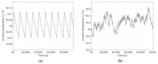
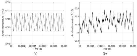
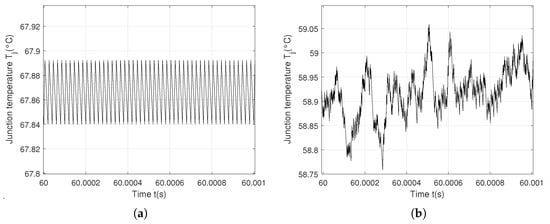
Figure 14, Figure 15 and Figure 16 show how different controllers of the Buck converter (at different frequencies) impacted the junction temperature evolutions (the stable period-1T and chaotic behaviors), however with an insignificant impact on the mean junction temperatures and their variations. This is explained by the presence of the same mean current as for the on-state MOSFET.
Figure 17 shows the distribution of power losses among the semiconductor MOSFET for periodic and chaotic operating points at different switching frequencies. MOSFETs incur losses every time they switch, so a higher switching frequency leads directly to higher losses. In this way, a higher switching frequency causes higher MOSFET and diode switching losses , (represented in blue and yellow bars). Even with the MOSFET switching only one time on the T period with controller (2) and many times with controller (3), the MOSFET and diode conduction losses , were nearly the same in all cases: they were not affected by the frequency or dynamical behaviors (periodic or chaotic), depending on the duty cycle. A very slight influence on the power values can be observed with the transition from the periodic to the chaotic regime (represented in red and green bars).
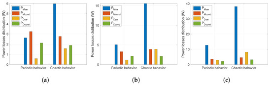
Figure 17.
(a) Power loss distribution for the periodic and chaotic behaviors at 10 kHz switching frequency; (b) power loss distribution for the periodic and chaotic behaviors at 20 kHz switching frequency; (c) power loss distribution for the periodic and chaotic behaviors at 50 kHz switching frequency.
4. Remaining Life Estimation
A thermal cycle counting algorithm was applied to the junction temperature in order to predict the remaining life of the power MOSFET. The most widely used algorithm is rainflow counting: it converts the time series of the junction temperature into a number of cycles, thereby facilitating lifetime prediction. In Figure 18a, the rainflow histogram presents a value of thermal cycles of 3000 × due to the periodicity. However, if the time series of the junction temperature is irregular or chaotic, the result of the rainflow counting algorithm is a set of organized cycles with a maximum of 120 × , as in Figure 18b.
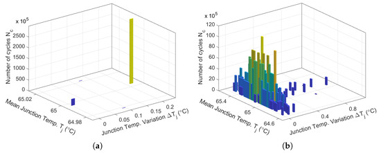
Figure 18.
(a) Thermal cycles considering and for a periodic behavior; (b) thermal cycles considering and for a chaotic behavior obtained with the rainflow counting algorithm.
Figure 19 and Figure 20 present the thermal cycles of the stable and chaotic behaviors of junction temperature at other frequencies f = 20 kHz and 50 kHz.
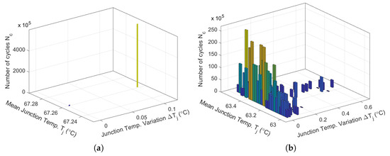
Figure 19.
(a) Thermal cycles considering and for a stable period-1T behavior; (b) thermal cycles considering and for a chaotic behavior obtained with the rainflow counting algorithm.
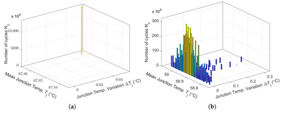
Figure 20.
(a) Thermal cycles considering and for a periodic behavior; (b) thermal cycles considering and for a chaotic behavior obtained with the rainflow counting algorithm.
These results were used to derive the MOSFET accumulated fatigue Q using the Miner’s rule. This is expressed as
where represents the number of cycles calculated using the rainflow counting algorithm, and is the number of cycles to failure. For the estimation of the device failure cycles, the Coffin–Manson equation was employed. It can be written as
where is the activation energy, A and are experimental coefficients, and k is the Boltzmann constant (8.617 × 10⁻⁵ eV/K).
An accelerated power cycling test was designed and experimentally executed to collect failure data. In a power cycling test, the device underwent repeated heating by conducting a predetermined current during the on-state, followed by a cooling period in the off-state, as illustrated in Figure 21a. Figure 21b includes a load current source, a measurement current source, and a gate voltage source. The device-heating load current was on for the ton duration and off during the cooling time toff. The experimental test involved long cycle times, where the MOSFET was switched on for 4 s and off for 12 s. A constant Ids was applied to maintain the junction temperature at 125 °C. A 100 mA measurement current was applied continuously to obtain the junction temperature. The gate voltage source controlled the device under test: 20 V were constantly applied to the gate. The heating and cooling process simulated real-world operational conditions, such as those found in electric vehicles. The periods of acceleration were followed by steady-speed cruising. The continuous cycles of heating and cooling induced the thermal stress that arises at the interface between materials with different coefficients of thermal expansion. For instance, stress can develop between silicon and aluminum layers due to their differing expansion behaviors under temperature variations, thus causing degradation. Consequently, power cycling imposes simultaneous electrical, thermal, and mechanical stress on the semiconductor die.
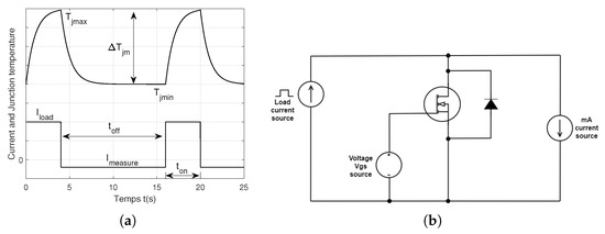
Figure 21.
(a) Top: temperature progression during power cycling; Bottom: current waveform for cycling profile, showing load current and small negative measurement current (the gate-source voltage follows the same pattern as the current); (b) Power cycling test circuit with gate switching.
The Coffin–Manson model considers the lifetime estimation and relies solely on and means, which are the main stress factors of the power device. The Coffin–Manson–Arrhenius, Lorris–Landzberg, Bayerer, Simplified Bayerer, CIPS08, and Schenermann models take into account electrical stress as dependent on the frequency f, on-time of one cycle , voltage V (sometimes included in the constant coefficient), current per bond feet I, bond wire diameter D, and wire bond aspect ratio of power cycle testing. It was observed that the device performance degradation varied from one unit to another due to minor discrepancies in manufacturing parameters. To evaluate the qualitative behavior of the C2M0080120D MOSFET, multiple devices were subjected to identical power cycling conditions.
However, due to inherent variations in the MOSFET’s characteristics – (Figure 22), differences in the mean and swing junction temperatures were observed across the tested devices. The junction temperatures recorded during three experimental tests were as follows: for the first test, = 127 °C, = 16 °C; the temperatures of the second test were = 126.5 °C, = 14.5 °C; and the last test’s temperatures were = 114.2 °C, = 12.5 °C. Failure of the device under test was recorded after = 8640 cycles, = 12,270 cycles, and = 25,400 cycles.
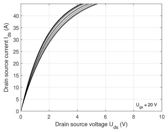
Figure 22.
The current–voltage characteristics of 10 devices.
These results were used to derive the experimental coefficients A and , as well as the activation energy . The logarithm function was applied to the Coffin–Manson equation, as in [52], using only three sets of experimental test data. Consequently, the development can be represented by
Hence, the thermal activation energy can be calculated from
The last coefficient can be written as
According to relations (14)–(16), the following numerical values were obtained: = −4.4887, = 0.0667, and A = 2.8823 × for a C2M0080120D MOSFET, as in [52]. With these coefficients and according to relation (13), the number of cycles to failure was for the stable period-1T behavior = 3.9064 × cycles calculated for = 65.05 °C and a extremely small = 0.21 °C; for the chaotic behavior, according to = 65.21 °C and = 0.87 °C, was found to be 1.2548 × . The degradation in the C2M0080120D MOSFET device at other frequencies is summed up in Table 3.
Table 3.
Accumulated fatigue results for the study cases.
The accumulated fatigue was insignificant for a stable period of the junction temperature , indicating a small impact on the remaining life of the MOSFET. The power losses were 10 times higher in the chaotic case than in the periodic regime. This power ratio resulted in a temperature variation six times higher in the chaotic case; it also generated a fatigue accumulation 100 times greater. However, only a small amount of damage was observed when the anticontrol of chaos feedback was applied. The repercussions of the chaotic temperature were small for the MOSFET thermal stress and reliability performance. The accumulated fatigue results show that the low- and high-frequency thermal cycles contributed in the same way to the aging of the Buck converter’s semiconductor. Thus, this leads to the conclusion that using anticontrol of chaos produced a very low accumulated fatigue effect of the Buck converter’s semiconductor. The accumulated fatigue results show that the low- and high-frequency thermal cycles contributed in the same way to the aging of the Buck converter’s semiconductor.
5. Conclusions
The target of this paper was to investigate the effects of the voluntary introduction of chaos into a Buck converter on the remaining life of power electronic switching components and their thermal stress. Indeed, a combination of anticontrol of chaos feedback with a standard PID controller introduced chaos into the circuit. The resulting effects involved complex dynamical behaviors, with a multitude of opportunities for special properties: maintaining a small ripple of the output voltage or even reducing it, and keeping a small swing current amplitude of the MOSFET and decreasing spectral emissions. Indeed, applying chaos anticontrol to switch-mode power supplies improved the performance, both in the frequency-domain and in the time-domaine. The results indicate that chaos had no impact on the mean junction temperature, but the temperature variation was six times higher in the chaotic case. Then, counting the thermal stress cycles allowed highlighting that the accumulated fatigue showed an insignificant degradation of the MOSFET lifetime with anticontrol of chaos feedback (in comparison to a standard controller), despite the fast switching of the MOSFET. Thus, this leads to the conclusion that using anticontrol of chaos produced a slight degradation in the remaining life of the semiconductor. Finally, future research demands, opportunities, and perspectives are identified here: to study the influence of anti-control of chaos on the reliability of capacitor and passive components, to integrate non-constant operating conditions such as ambient temperature. Online monitoring, along with prognostics and health management (PHM), are critical areas that require thorough analysis and development.
Author Contributions
Conceptualization, C.M.; Methodology, C.M.; Software, C.M.; Validation, C.M. and J.-Y.M.; Writing—original draft preparation, C.M. and J.-Y.M.; Writing—review and editing, C.M. and J.-Y.M. All authors have read and agreed to the published version of the manuscript.
Funding
This research received no external funding.
Data Availability Statement
The data are available upon request to the corresponding author.
Conflicts of Interest
The authors declare no conflicts of interest.
References
- Minati, L.; Innocenti, G.; Mijatovic, G.; Ito, H.; Frasca, M. Mechanisms of chaos generation in an atypical single-transistor oscillator. Chaos Solitons Fractals 2022, 157, 111878. [Google Scholar] [CrossRef]
- Chen, X.; Long, X.; Hu, W.; Xie, B. Bifurcation and chaos behaviors of Lyapunov function controlled PWM boost converter. Energy Rep. 2021, 7, 163–168. [Google Scholar] [CrossRef]
- Zamani, N.; Ataei, M.; Niroomand, M. Analysis and control of chaotic behavior in boost converter by ramp compensation based on Lyapunov exponents assignment: Theoretical and experimental investigation. Chaos Solitons Fractals 2015, 81, 20–29. [Google Scholar] [CrossRef]
- Dhifaou, R.; Brahmi, H. Fast Simulation and Chaos Investigation of a DC-DC Boost Inverter. Complexity 2021, 9162259. [Google Scholar] [CrossRef]
- Ghosh, A.; Banerjee, S.; Basak, S.; Chakraborty, C. A study of chaos and bifurcation of a current mode controlled flyback converter. In Proceedings of the IEEE 23rd International Symposium on Industrial Electronics (ISIE), Istanbul, Turkey, 1–4 June 2014. [Google Scholar]
- Morel, C.; Akrad, A.; Sehab, R.; Azib, T.; Larouci, C. Open-Circuit Fault-Tolerant Strategy for Interleaved Boost Converters via Filippov Method. Energies 2022, 15, 352. [Google Scholar] [CrossRef]
- Morel, C.; Morel, J.-Y.; Danca, M.F. Generalization of the Filippov method for systems with a large periodic input. Math. Comput. Simul. 2018, 146, 1–13. [Google Scholar] [CrossRef]
- Trujillo, S.C.; Candelo-Becerra, J.E.; Hoyos, F.E. Analysis and Control of Chaos in the Boost Converter with ZAD, FPIC, and TDAS. Symmetry 2022, 14, 13170. [Google Scholar] [CrossRef]
- Morel, C.; Vlad, R.C.; Morel, J.-Y. Similarities between the Lorenz Related Systems. Nonlinear Dyn. Syst. Theory 2022, 22, 66–81. [Google Scholar]
- Wu, J.; Zeng, Y.; Zhou, P.; Li, N. Broadband chaos generation in VCSELs with intensity-modulated optical injection. Opt. Laser Technol. 2023, 159, 108994. [Google Scholar] [CrossRef]
- Gong, X.; Wang, H.; Ji, Y.; Zhang, Y. Optical chaos generation and synchronization in secure communication with electro-optic coupling mutual injection. Opt. Commun. 2022, 521, 128565. [Google Scholar] [CrossRef]
- Yin, T.; Wang, Y. Predicting the price of WTI crude oil futures using artificial intelligence model with chaos. Fuel 2022, 316, 122523. [Google Scholar] [CrossRef]
- He, J.; Yu, S.; Cai, J. Topological horseshoe analysis for a three-dimensional anti-control system and its application. Optik 2016, 127, 9444–9456. [Google Scholar] [CrossRef]
- Erkan, E.; Ogras, H.; Fidan, S. Application of a secure data transmission with an effective timing algorithm based on LoRa modulation and chaos. Microprocess. Microsyst. 2023, 99, 104829. [Google Scholar] [CrossRef]
- Wen, H.; Lin, Y.; Yang, L.; Chen, R. Cryptanalysis of an image encryption scheme using variant Hill cipher and chaos. Expert Syst. Appl. 2024, 250, 123748. [Google Scholar] [CrossRef]
- Raiesdana, S.; Mohammad Hashemi Goplayegani, S. Study on chaos anti-control for hippocampal models of epilepsy. Neurocomputing 2013, 111, 54–69. [Google Scholar] [CrossRef]
- Borah, M.; Das, D.; Gayan, A.; Fenton, F.; Cherry, E. Control and anticontrol of chaos in fractional-order models of Diabetes, HIV, Dengue, Migraine, Parkinson’s and Ebola virus diseases. Chaos Solitons Fractals 2021, 153, 111419. [Google Scholar] [CrossRef]
- Dong, Y.; Yang, S.; Liang, Y.; Wang, G. Neuromorphic dynamics near the edge of chaos in memristive neurons. Chaos Solitons Fractals 2022, 160, 112241. [Google Scholar] [CrossRef]
- Choudhary, D.; Foster, K.R.; Uphoff, S. Chaos in a bacterial stress response. Curr. Biol. 2023, 33, 5404–5414. [Google Scholar] [CrossRef]
- Luo, S.; Li, S.; Tajaddodianfar, F.; Hu, J. Anti-oscillation and chaos control of the fractional-order brushless DC motor system via adaptive echo state networks. J. Frankl. Inst. 2018, 355, 6435–6453. [Google Scholar] [CrossRef]
- Yan, Z.; Li, Y.; Eslami, M. Maximizing micro-grid energy output with modified chaos grasshopper algorithms. Heliyon 2024, 10, e23980. [Google Scholar] [CrossRef]
- Ru, X. Parameter extraction of photovoltaic model based on butterfly optimization algorithm with chaos learning strategy. Sol. Energy 2024, 269, 112353. [Google Scholar] [CrossRef]
- Elmasry, Y.; Chaturvedi, R.; Solomin, E.; Smaisim, G.F.; Hadrawi, S.K. The numerical analysis to assess the second-law features of a solar water heater equipped with a dual-twisted tape turbulator; Developing a predictive model for useful thermal exergy based on the nonlinear calibration using the Chaos Control Method (CCM). Eng. Anal. Bound. Elem. 2024, 159, 37–383. [Google Scholar] [CrossRef]
- Lin, F.L.; Chen, D.Y. Reduction of Power Supply EMI Emission by Switching Frequency Modulation. IEEE Trans. Power Electron. 1994, 9, 132–137. [Google Scholar]
- Stankovic, A.M.; Verghese, G.C.; Perreault, D.J. Analysis and Synthesis of Randomized Modulation Schemes for Power Converters. IEEE Trans. Power Electron. 1995, 10, 680–693. [Google Scholar] [CrossRef]
- Deane, J.H.B.; Ashwin, P.; Hamill, D.C.; Jefferies, D.J. Calculation of the Periodic Spectral Components in a Chaotic DC-DC Converter. IEEE Trans. Circuits Syst.-I Fundam. Theory Appl. 1999, 46, 1313–1319. [Google Scholar] [CrossRef]
- Woywode, O.; Guldner, H.; Baranovski, A.L.; Schwarz, W. Bifurcation and Statistical Analysis of DC-DC Converters. IEEE Trans. Circuits Syst.-I Fundam. Theory Appl. 2003, 50, 1072–1080. [Google Scholar] [CrossRef]
- Morel, C.; Bourcerie, M.; Chapeau-Blondeau, F. Generating independent chaotic attractors by chaos anticontrol in nonlinear circuits. Chaos Solitons Fractals 2005, 26, 541. [Google Scholar] [CrossRef][Green Version]
- Morel, C.; Vlad, R.; Morel, J.-Y. Anticontrol of Chaos Reduces Spectral Emissions. J. Comput. Nonlinear Dyn. 2008, 3, 041009. [Google Scholar] [CrossRef]
- Li, H.; Zhang, B.; Li, Z.; Halang, W.A.; Chen, G. Controlling DC–DC converters by chaos-based pulse width modulation to reduce EMI. Chaos Solitons Fractals 2009, 42, 1378–1387. [Google Scholar] [CrossRef]
- Vidya, P.M.; Sudha, S. A fully integrated VLSI architecture using chaotic PWM for RF transmitter design with electromagnetic interference reduction. Integration 2022, 83, 33–45. [Google Scholar] [CrossRef]
- Chen, Y.; Xing, B.; He, G.; Jiang, W.; Wang, Z. Research on EMI suppression of high frequency isolate quasi-Z-source inverter based on chaotic frequency modulation. Energy Rep. 2022, 8, 10363–10371. [Google Scholar] [CrossRef]
- Morel, C.; Rizoug, N. Electro-Thermal Modeling, Aging and Lifetime Estimation of Power Electronic MOSFETs. Civ. Eng. Res. J. 2022, 14, 555879. [Google Scholar] [CrossRef]
- Hu, Z.; Zhang, W.; Wu, J. An Improved Electro-Thermal Model to Estimate the Junction Temperature of IGBT Module. Electronics 2019, 8, 1066. [Google Scholar] [CrossRef]
- Zheng, J.; Zheng, Z.; Xu, H.; Liu, W.; Zeng, Y. Accurate Time-segmented Loss Model for SiC MOSFETs in Electro-thermal Multi-Rate Simulation. arXiv 2023, arXiv:2311.07029. [Google Scholar]
- Jahdi, S.; Alatise, O.; Ran, L.; Mawby, P. Accurate analytical modeling for switching energy of PiN diodes reverse recovery. IEEE Trans. Ind. Electron. 2015, 62, 1461–1470. [Google Scholar] [CrossRef]
- Zhaksylyk, A.; Rauf, A.-M.; Chakraborty, S.; El Baghdadi, M.; Geury, T.; Ciglaric, S.; Hegazy, O. Evaluation of Model Predictive Control for IPMSM Using High-Fidelity Electro-Thermal Model of Inverter for Electric Vehicle Applications. Proc. SAE WCX Digit. 2021, 37, 290–295. [Google Scholar]
- Ma, K.; Bahman, A.S.; Beczkowski, S.; Blaabjerg, F. Complete Loss and Thermal Model of Power Semiconductors Including Device Rating Information. IEEE Trans. Power Electron. 2015, 30, 290–295. [Google Scholar] [CrossRef]
- Górecki, K.; Zarębski, J.; Górecki, P. Influence of Thermal Phenomena on the Characteristics of Selected Electronics Networks. Energies 2021, 14, 4750. [Google Scholar] [CrossRef]
- Zhou, Z.; Kanniche, M.S.; Butcup, S.G.; Igic, P. High-speed electrothermal simulation model of inverter power modules for hybrid vehicles. IEEE Trans. Ind. Electron. 2011, 5, 636–643. [Google Scholar]
- Górecki, P.; Wojciechowski, D. Accurate Electrothermal Modeling of High Frequency DC–DC Converters with Discrete IGBTs in PLECS Software. IEEE Trans. Ind. Electron. 2023, 70, 5739–5746. [Google Scholar] [CrossRef]
- Górecki, P.; d’Alessandro, V. A Datasheet-Driven Electrothermal Averaged Model of a Diode–MOSFET Switch for Fast Simulations of DC–DC Converters. Electronics 2024, 13, 154. [Google Scholar] [CrossRef]
- Karami, M.; Li, T.; Tallam, R.; Cuzner, R. Thermal Characterization of SiC Modules for Variable Frequency Drives. IEEE Open J. Power Electron. 2021, 2, 336–345. [Google Scholar] [CrossRef]
- Chen, H.; Lin, S.; Liu, Y. Transient electro-thermal coupled modeling of three-phase power MOSFET inverter during load cycles. Materials 2021, 14, 5427. [Google Scholar] [CrossRef]
- Nayak, D.P.; Pramanick, S.K. Implementation of an Electro-Thermal Model for Junction Temperature Estimation in a SiC MOSFET Based DC/DC Converter. CPSS Trans. Power Electron. Appl. 2023, 8, 42–53. [Google Scholar] [CrossRef]
- Urkizu, J.; Mazura, M.; Alacano, A.; Aizpuru, I.; Chakraborty, S. Electric vehicle inverter electro-thermal models oriented to simulation speed and accuracy multi-objective targets. Energies 2019, 12, 3608. [Google Scholar] [CrossRef]
- Cao, R. A Thermal Modeling of Power Semiconductor Devices with Heat Sink Considering Ambient Temperature Dynamic. In Proceedings of the IEEE 9th International Power Electronics and Motion Control Conference (IPEMC2020-ECCE Asia), Nanjing, China, 29 November 2020–2 December 2020; Volume 37, pp. 290–295. [Google Scholar]
- Kishor, Y.; Patel, R. Thermal modeling and reliability analysis of recently introduced high gain converters for PV application. Clean. Energy Syst. 2022, 3, 100016. [Google Scholar] [CrossRef]
- Sangwongwanich, A.; Yang, Y.; Sera, D.; Blaabjerg, F. Lifetime Evaluation of Grid-Connected PV Inverters Considering Panel Degradation Rates and Installation Sites. IEEE Trans. Power Electron. 2018, 33, 1225–1236. [Google Scholar] [CrossRef]
- Shen, Y.; Chub, A.; Wang, H.; Vinnikov, D.; Liivik, E.; Blaabjerg, F. Wear-Out Failure Analysis of an Impedance-Source PV Microinverter Based on System-Level Electrothermal Modeling. IEEE Trans. Ind. Power Electron. 2019, 66, 3914–3927. [Google Scholar] [CrossRef]
- Shipurkar, U.; Lyrakis, E.; Ma, K.; Polinder, H.; Ferreira, J.A. Lifetime Comparison of Power Semiconductors in Three-Level Converters for 10-MW Wind Turbine Systems. IEEE J. Emerg. Sel. Top. Power Electron. 2018, 6, 1366–1377. [Google Scholar] [CrossRef]
- Morel, C.; Morel, J.-Y. Impact of Chaos on MOSFET Thermal Stress and Lifetime. Electronics 2024, 13, 1649. [Google Scholar] [CrossRef]
- Stella, F.; Pellegrino, G.; Member, S.; Armando, E.; Dapr, D. Online junction temperature estimation of SiC power MOSFETS through onstate voltage mapping. IEEE Trans. Ind. Appl. 2018, 54, 3453–3462. [Google Scholar] [CrossRef]
- Baker, N.; Munk-Nielsen, S.; Iannuzzo, F.; Liserre, M. IGBT junction temperature measurement via peak gate current. IEEE Trans. Power Electron. 2016, 31, 3784–3793. [Google Scholar] [CrossRef]
- Barlini, D.; Ciappa, M.; Castellazzi, A.; Mermet-Guyennet, M.; Fichtner, W. New technique for the measurement of the static and of the transient junction temperature in IGBT devices under operating conditions. Microelectron. Reliab. 2006, 46, 1772–1777. [Google Scholar] [CrossRef]
- Bryant, A.; Yang, S.; Mawby, P.; Xiang, D.; Ran, L.; Tavner, P.; Palmer, P.R. Investigation into IGBT dv/dt during turn-off and its temperature dependence. IEEE Trans. Power Electron. 2011, 26, 3019–3031. [Google Scholar] [CrossRef]
- Luo, H.; Li, W.; Iannuzzo, F.; He, X.; Blaabjerg, F. Enabling junction temperature estimation via collector-side thermo-sensitive electrical parameters through emitter stray inductance in high-power igbt modules. IEEE Trans. Ind. Electron. 2018, 65, 4724–4738. [Google Scholar] [CrossRef]
- Yang, F.; Pu, S.; Xu, C.; Akin, B. Turn-on delay based real-time junction temperature measurement for SiC MOSFETs with aging compensation. IEEE Trans. Power Electron. 2021, 36, 1280–1294. [Google Scholar] [CrossRef]
- Zhang, Z.; Dyer, J.; Wu, X.; Wang, F.; Costinett, D.; Tolbert, L.M.; Blalock, B.J. Online junction temperature monitoring using intelligent gate drive for SiC power devices. IEEE Trans. Power Electron. 2019, 34, 7922–7932. [Google Scholar] [CrossRef]
- Dini, P.; Ariaudo, G.; Botto, G.; La Greca, F.; Saponara, S. Real-time electro-thermal modelling and predictive control design of resonant power converter in full electric vehicle applications. IET Power Electron. 2023, 16, 2045–2064. [Google Scholar] [CrossRef]
- Dini, P.; Basso, G.; Saponara, S.; Romano, C. Real-time monitoring and ageing detection algorithm design with application on SiC-based automotive power drive system. IET Power Electron. 2024, 17, 690–710. [Google Scholar] [CrossRef]
- Wolfspeed. C2M0080120D Silicon Carbide Power MOSFET C2M MOSFET Technology; Product datasheet. Datasheet, Rev. 5; Wolfspeed: Durham, NC, USA, 2023; pp. 1–11. [Google Scholar]
- Peng, M. Symmetry breaking, bifurcations, periodicity and chaos in the Euler method for a class of delay differential equations. Chaos Solitons Fractals 2005, 24, 1287–1297. [Google Scholar] [CrossRef]
- Morel, C.; Vlad, R.; Morel, J.-Y.; Petreus, D. Generating chaotic attractors on a surface. Math. Comput. Simul. 2011, 81, 2549–2563. [Google Scholar] [CrossRef][Green Version]


Disclaimer/Publisher’s Note: The statements, opinions and data contained in all publications are solely those of the individual author(s) and contributor(s) and not of MDPI and/or the editor(s). MDPI and/or the editor(s) disclaim responsibility for any injury to people or property resulting from any ideas, methods, instructions or products referred to in the content. |
© 2025 by the authors. Licensee MDPI, Basel, Switzerland. This article is an open access article distributed under the terms and conditions of the Creative Commons Attribution (CC BY) license (https://creativecommons.org/licenses/by/4.0/).