1. Development Trend of Solid State Actuators
Development of solid state actuators aimed at replacing conventional electromagnetic motors has been remarkable in the following three areas: precision positioning, vibration suppression and miniature motors. Particular attention has been given to piezoelectric/electrostrictive ceramic actuators, shape memory devices of alloys such as Ni-Ti and Cu-Zn-Al, and magnetostrictive actuators using Terfenol D (Tb-Fe-Dy) alloys. Rigid strains induced in a piezoelectric ceramic by an external electric field have been used as ultraprecision cutting machines, in the Hubble telescope on the space shuttle and in dot-matrix printer heads [
1,
2,
3,
4,
5]. There has also been proposed a parabolic antenna made of shape memory alloy, which is in a compactly folded shape when first launched on an artificial satellite, and subsequently recovers its original shape in space when exposed to the heat of the sun. Smart skins on submarines or military tanks were targets for solid state actuators [
6].
In general, thermally-driven actuators such as shape memory alloys can show very large strains, but require large drive energy and exhibit slow response. Magnetic field-driven magnetostrictive devices have serious problems with size because of the necessity for the magnetic coil and shield. The subsequent Joule heat causes thermal dilatation in the system, and leakage magnetic field sometimes interferes with the operating hybrid electronic circuitry. On the contrary, electric field-driven piezoelectric and electrostrictive actuators have been most developed because of their high efficiency, quick response, compact size, no generation of heat or magnetic field, in spite of relatively small induced strains.
This article reviews shape memory properties of ceramics, focusing on antiferroelectric lead zirconate titanate (Pb(Zr,Ti)O3, PZT) based ceramics. The shape memory effect can be observed, not only in special alloys and polymers, but also in ceramics such as partially stabilized zirconia and ferroelectric lead zirconate titanate. A new concept of “shape memory” is proposed in this article: the elastic strain change associated with the electric field-induced phase transition is utilized instead of stress-induced or thermally-induced phase transitions, which enables many smarter actuator applications than the normal piezoelectrics or electrostrictors.
The principle of the ceramic shape memory effect is described firstly in comparison with the case of alloys. Phase diagrams, domain reversal mechanisms and fundamental actuator characteristics are then discussed, followed by the practical distinctions between these new ceramics and shape memory alloys. Phenomenological explanations are described on the field-induced strain jump associated with the phase transformation, and on the piezoelectric anisotropy in a two-sublattice polarization coupling model. Finally, possible unique applications are proposed including a latching relay and a mechanical clamp.
This review paper is to provide author’s comprehensive idea on the AFE-FE phase transition by coupling experimental results [
7] and theoretical approach [
8].
2. Shape Memory Ceramics
Shape memory effect is observed not only in special alloys or polymers, but also in ceramics. The shape memory effect in alloys (such as NiTiNOL) originates from a thermally-induced or stress-induced “martensitic” phase transformation. After the alloy is deformed largely in the martensitic state, this apparently permanent strain is recovered to its original shape when heated to cause the reverse martensitic transition. Then, upon cooling, the shape returns to its original state (
Figure 1a).
A similar effect is anticipated in ceramics with a certain phase transition,
i.e., a “ferroelastic” phase transition. Reyes-Morel
et al. demonstrated the shape memory effect, as well as superelasticity in a CeO
2-stabilized tetragonal zirconia (ZrO
2) polycrystal [
9]. Under uniaxial compression, the specimen deforms plastically owing to a stress-induced tetragonal to monoclinic transition in Ce-doped zirconia. Continuous deformation is interrupted by repeated load drops, providing a nearly constant upper yield stress of 0.7 GPa. Even after unloading, large residual plastic axial strain (≈0.7%) is observed. Subsequent heating produces a gradual recovery of the residual strain due to the reverse phase transition starting at 60 °C and a burst of strain recovery at 186 °C. The burst is very sharp, above which approximately 95% of the prior axial strain is recovered. Though recent conventional shape memory studies based on Martensitic phase transformation in structural ceramics can be found [
10], we do not discuss them because they are out of our objective; that is, electric-field controllable shape memory.
Ceramics “shape memory” has also been reported for certain ferroelectricity-related transitions, namely paraelectric–ferroelectric [
11] and antiferroelectric (AFE)–ferroelectric (FE) transitions [
12,
13]. The former thermally-induced transition revealed a shape-recovery phenomenon similar to zirconia ceramics. On the contrary, the latter is related to an electric field-induced transition, and exhibits large displacement (0.4%) with a “digital” characteristic or a shape memory function, which is in contrast to the essentially “analogue” nature of conventional piezoelectric and electrostrictive strains with 0.1% in magnitude (
Figure 1b). Note that the “memory” terminology is different in the AFE shape memory; that is, field-induced FE expanded shape is “memorized” even after removing the field, and to recover the original AFE small shape, we apply a small reverse electric field.
Let us review ferroelectricity and antiferroelectricity here for further understanding [
14].
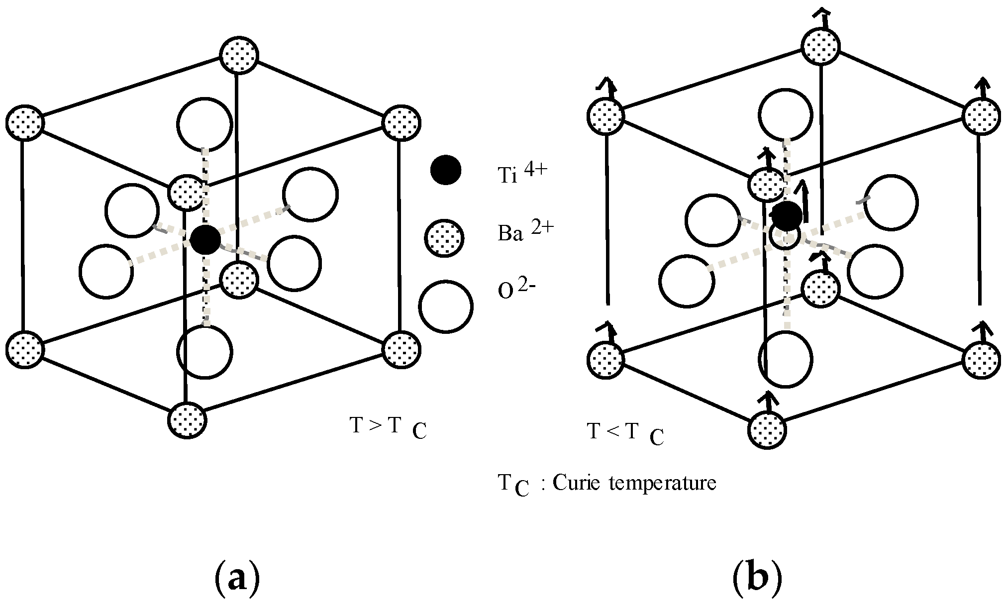
Figure 2 shows the crystal structure changes in a typical ferroelectric, barium titanate (BaTiO
3, BT). At an elevated temperature above the transition point of 130 °C (Curie temperature, denoted as T
C), BT shows a cubic “perovskite” structure (paraelectric (PE) phase), as illustrated in
Figure 2a. With decreasing temperature below T
C, the cations (Ba
2+ and Ti
4+) shift against the anions (O
2−) as illustrated in
Figure 2b, exhibiting spontaneous polarization as well as spontaneous strain (ferroelectric (FE) phase). Notice that the electric dipole moments in each crystal unit cell are arranged in parallel in a ferroelectric. On the other hand, there exists an antiferroelectric where the dipoles are arranged antiparallel to each other so as not to produce net polarization.
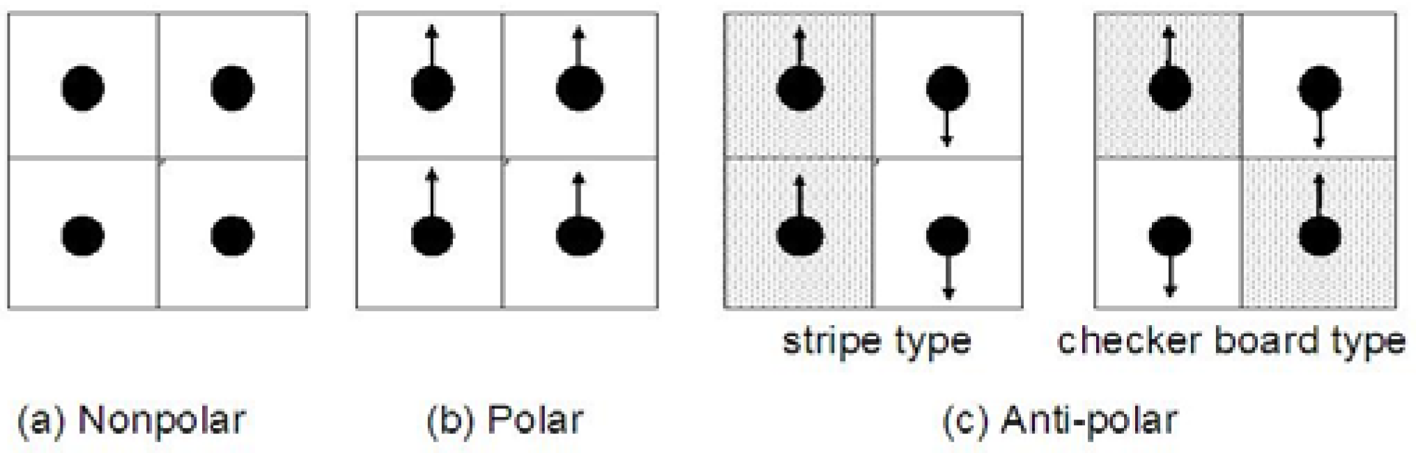
Figure 3 shows the antipolar dipole arrangement models in contrast to nonpolar and polar models.
When the free energy of the antipolar state is close to the energy of the polar state, the dipole configuration is rearranged by the external electric field or stress.
Figure 4 shows the applied electric field
versus induced polarization curves in PE, FE and AFE materials. A linear relation and a hysteresis due to the spontaneous polarization reversal between positive and negative directions are observed in a PE and in a FE, respectively. On the contrary, an AFE exhibits an electric field-induced phase transition to a FE state above a critical field E
t, accompanied by a hysteresis above E
t. Reducing the field down to zero, the remanent polarization is not observed, providing a so-called “double hysteresis” curve in total. A large strain jump is theoretically associated with this phase transition, which also appears as a double hysteresis. In a certain case, once the FE state is induced, this FE state is sustained even if the electric field is decreased to zero; this corresponds to the “shape memory” phenomenon. The mechanism for the shape memory effect in the AFE ceramics is schematically illustrated in
Figure 1b.
3. Sample Preparation and Experiments
This section introduces sample preparation and experimental procedures of shape memory ceramics. Antiferroelectric perovskite ceramics from the PZT system (PbZrO
3 rich compositions) have been investigated, in which successive phase transitions from a PE, through an AFE, to a FE state appear with decreasing temperature [
15]. PZT ceramics Pb
0.99Nb
0.02[(Zr
0.6Sn
0.4)
1-yTi
y]
0.98O
3 (0.05 < y < 0.09) (abbreviated hereafter as PNZST) were prepared from reagent grade oxide raw materials, PbO, Nb
2O
5, ZrO
2, SnO
2 and TiO
2. We introduced “Sn” to stabilize the antiferroelectric phase, and “Nb” to increase the sinterability basically. Bulk samples were prepared by hot-press sintering at 1200 °C. Unimorphs were fabricated with two thin rectangular plates (22 mm
7 mm
0.2 mm thick) bonded together. Multilayer samples (12 mm
4.3 mm
4.3 mm thick) with each layer 140 μm in thickness were also fabricated using the tape casting technique: Those with platinum electrodes were sintered at a temperature of about 1250 °C.
The field-induced lattice change was determined by X-ray diffraction. The surfaces of the thin ceramic plate (t = 0.2 mm) were coated with carbon evaporated electrode. X-ray diffraction patterns were recorded at the electrode surface for several different bias voltages. The displacement or strain induced by an alternating electric field (0.05 Hz) was detected with a strain gauge (Kyowa Dengyo, Tokyo, Japan, KFR-02-C1-11), a magneto-resistive potentiometer (Midori Precisions, Tokyo, Japan, LP-1 U) or a differential transformer-type (Millitron, Tokyo, Japan, No. 1202). For the dynamic displacement in unimorphs, a noncontact-type eddy current displacement sensor (Kaman, Colorado Springs, CO, USA, KD-2300) was used. The electric polarization and the permittivity were measured with a Sawyer–Tower circuit and an impedance analyzer (Hewlett-Packard, now Agilent, Santa Clara, CA, USA, 4192A), respectively. To observe the domain structures, a CCD microscope with a magnification of
1300 was applied to a thinly-sliced sample of large grain (>50 μm) PNZST ceramics with interdigital electrodes on the surface.
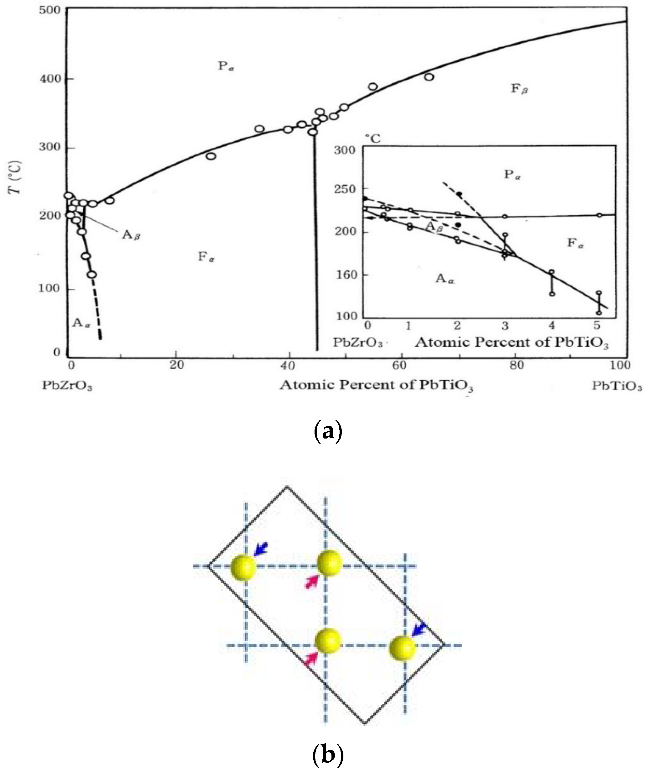
Figure 5a shows a PZT phase diagram with a particular interest in PbZrO
3 (PZ) rich region, and
Figure 5b illustrates the Pb
2+ ionic shift in a PZ unit cell to visualize the antipolar structure [
16].
4. Fundamental Properties of the Electric Field-Induced Phase Transition
The antiparallel arrangement of electric dipoles in the sublattices of AFE is rearranged in parallel by an applied electric field, and the dielectric and electromechanical properties are changed remarkably at this phase change.
4.1. Electric Field Dependence of Lattice Parameters
The field-induced change in lattice parameters for a sample Pb
0.99Nb
0.02[(Zr
0.6Sn
0.4)
1-yTi
y]
0.98O
3 with y = 0.06 is plotted in
Figure 6a [
7]. The forced transition from the AFE to the FE phase gives rise to the simultaneous increase of
a and
c in the perovskite unit cell, thereby keeping the tetragonality,
c/a, nearly constant. Since the angle γ makes only a negligible contribution to the volume change, the strain change at the phase transition is nearly isotropic with a magnitude of Δ
L/L = 8.5 × 10
−4. Though we observe minor changes in the parameters
c,
c/
a and γ between AFE-FE On-set and FE-AFE Off-set electric fields, we cannot discuss further on this, because the measurement was made on a polycrystalline sample and the effective electric field on a certain crystal orientation in each grain was distributing.
The intensity change of the X-ray reflections with the application of an electric field suggests that the spontaneous polarization in the FE state lies in the c-plane, parallel with the perovskite [1 1 0] axis, and that the sublattice polarization configuration in the AFE state is very similar to that of PbZr0
3 (see
Figure 5b) [
16].
Figure 6b illustrates the simplest two-sublattice model.
4.2. Temperature Dependence of the Permittivity
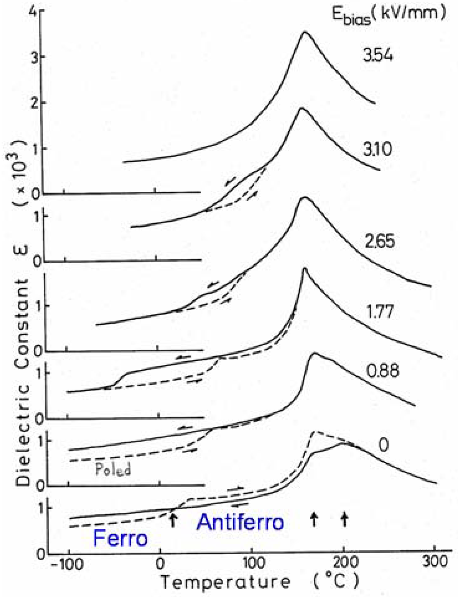
Figure 7 shows change of permittivity with temperature under various bias electric field in a composition y = 0.06, Pb
0.99Nb
0.02[(Zr
0.6Sn
0.4)
0.94Ti
0.06]
0.98O
3 [
7]. With an increase in temperature the ferro- to antiferroelectric phase transition is clearly observed in a poled specimen as a permittivity hump. Note that the reverse antiferro- to ferroelectric transition occurs with a considerably large hysteresis with temperature decreasing. Though we observe another narrow pseudo-cubic antiferroelectric phase (which may correspond to A
β Phase in
Figure 5a) just below the Neel temperature under small bias electric field, we will not discuss its details in this paper.
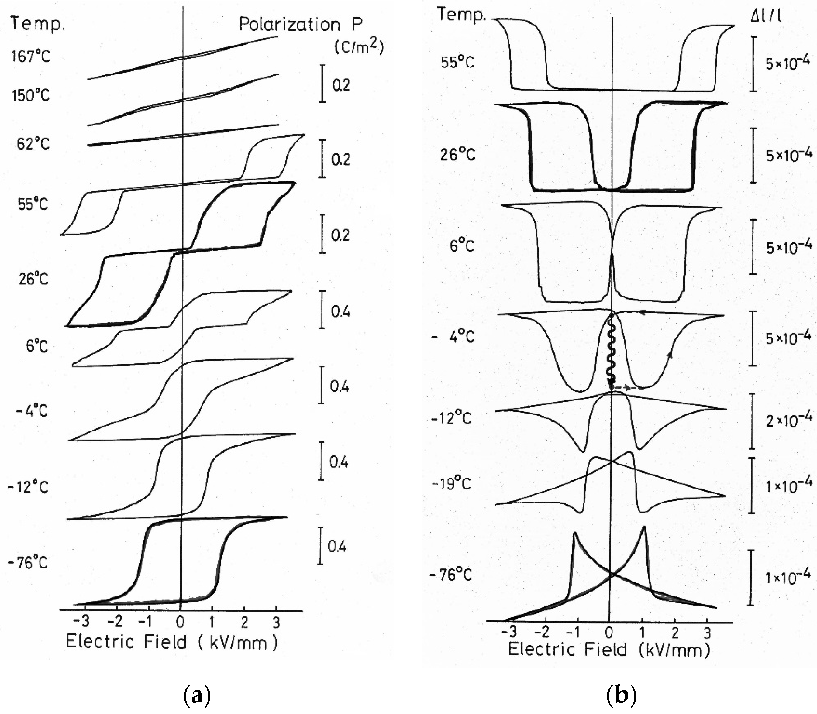
Figure 8a shows the relation between the electric field and polarization. The typical double and ferroelectric hysteresis loops are observed at room temperature and −76 °C, respectively, while a transitive shape with humps is observed at intermediate temperatures.
The transitive process can be observed more clearly in the strain curve.
Figure 8b shows the transversely induced strains. The forced transition from AFE to FE at room temperature is characterized by a huge strain discontinuity. On the other hand, a typical ferroelectric butterfly-type hysteresis is observed at −76 °C, corresponding to polarization reversal. It is important to note that the strain discontinuities associated with the phase transition have the same positive expansion in both longitudinal and transverse directions with respect to the electric field (
i.e., the apparent Poisson’s ratio is negative!), while the piezo-striction is negative and positive in the transverse and longitudinal directions, respectively, which will further be discussed in
Section 4.4.
The shape memory effect is observed on this loop at −4 °C. When a large electric field is applied to the annealed AFE sample, a massive strain ΔL/L of about 7 × 10⁻⁴ is produced and maintained metastably even after the field is removed. After applying a small reverse field or thermal annealing, the original AFE shape is observed.
The reverse critical field related to the FE-AFE transition is plotted with solid lines in the phase diagram for the sample with y = 0.06 in
Figure 9, in which the temperature-field points are based on the measurements in permittivity, polarization and strain. In the temperature range from −30 °C to 10 °C, a hump-type hysteresis in the field
versus polarization curve and an inverse hysteresis in the field-induced strain are observed: this has previously often been misinterpreted as another AFE phase different from the phase above 10 °C. The annealed state below −30 °C down to −200 °C is AFE. However, once the FE state is induced, the AFE phase is never observed during a cycle of rising and falling electric field. The critical field line for the FE to AFE transition (the solid line) in the temperature range −30 °C to 10 °C intersects the coercive field line for the + FE to − FE reversal (the dashed line) below −30 °C.
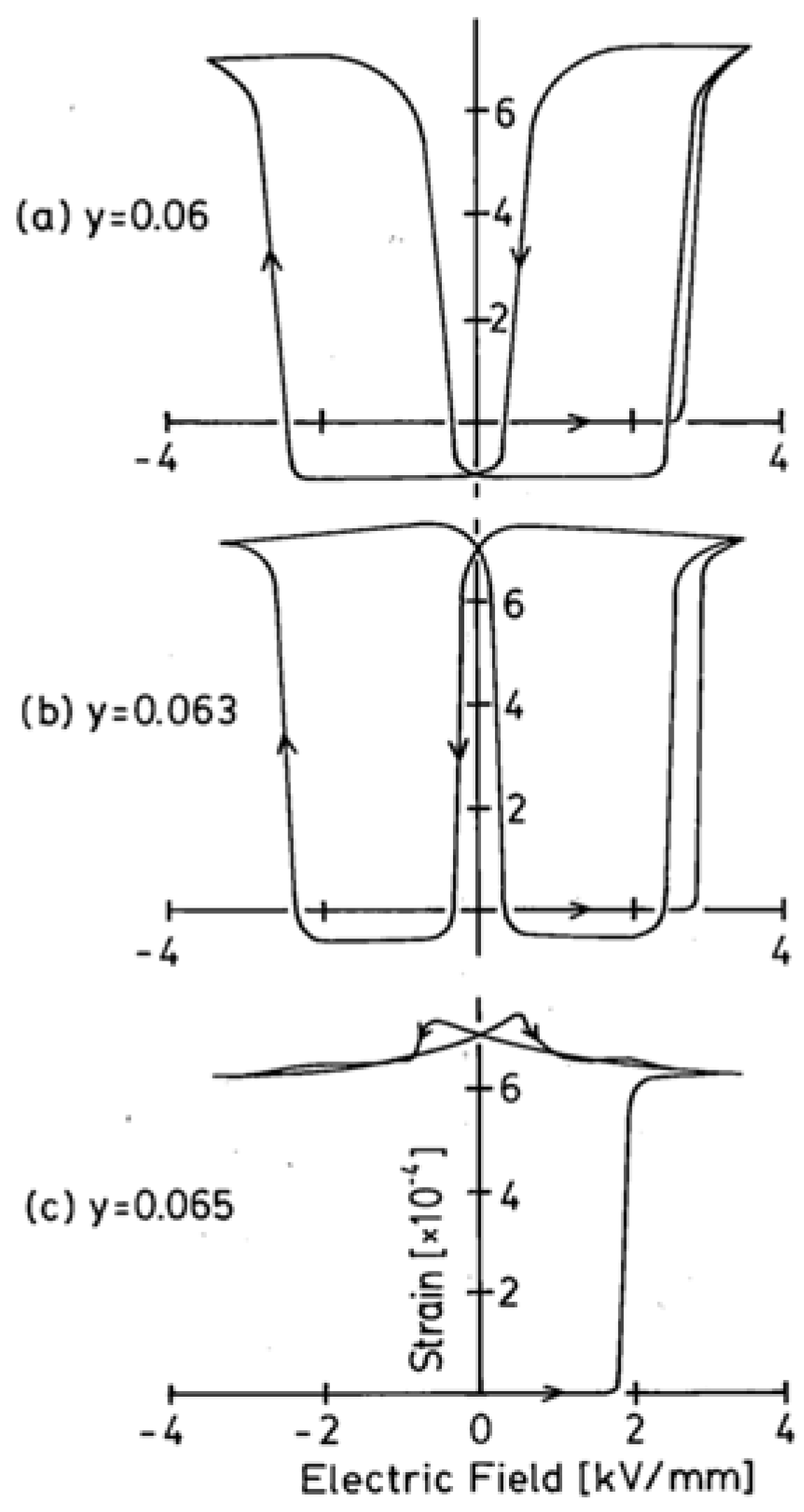
4.3. Composition Dependence of the Induced Strain
Figure 10 shows the strain curves induced transversely by the external field at room temperature for samples of several different compositions [
8]. The molar fraction of Ti,
y, is increased from 0.06 (
Figure 10a) to 0.065 (
Figure 10c). The initial state was obtained by annealing at 150 °C, which is above the Curie (or Neel) temperature for all the samples. A typical double hysteresis curve (Type I) is observed in the sample containing y = 0.06. Large jumps in the strain are observed at the forced phase transitions from the AFE to the FE phase (Δ
L/L = 8 × 10
−4). In comparison, the strain change with electric field in either the AFE or FE state is rather small: this suggests a possible application for the material as a “digital” displacement transducer, having OFF/ON displacement states. The difference in the strain between that occurring in the initial state and that appearing in a cyclic process at E = 0 kV/cm is also noteworthy and will be explained in the following section.
In the sample with y = 0.063, a Ti concentration slightly higher than that just described, the field-induced FE phase will not return to the AFE state even after decreasing the field to zero (Type II,
Figure 10b): this is called “memorizing” the FE strain state. In order to obtain the initial AFE state, a small reverse bias field is required.
Figure 10c shows the strain curve for the sample with y = 0.065, which exhibits irreversible characteristics during an electric field cycle (Type III). The initial strain state can only be recovered by thermal annealing up to 50 °C.
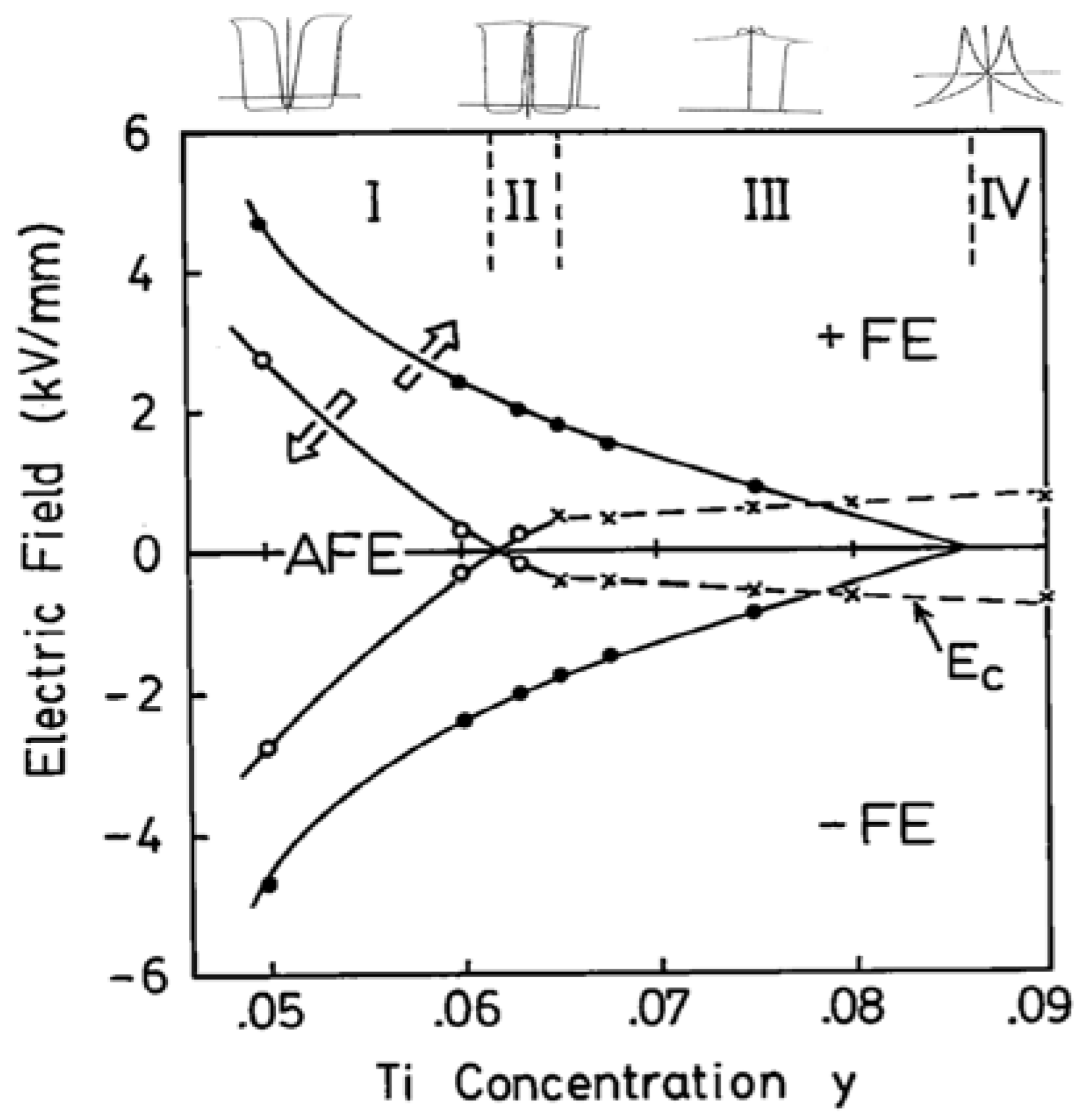
Data derived from these strain curves may be utilized to construct a phase diagram of the system Pb
0.99Nb
0.02[(Zr
0.6Sn
0.4)
1-yTi
y]
0.98O
3 at room temperature with respect to the composition y and the applied electric field E (
Figure 11). If the Ti concentration of the horizontal axis is redefined in terms of temperature and evaluated in the opposite direction, this phase diagram is topologically the same as the phase diagram of
Figure 9. The key feature of this phase diagram is the existence of the three phases, namely the AFE, the positively poled FE (+ FE), and the negatively poled FE (− FE) phases, the boundaries of which are characterized by the two transition lines corresponding to rising and falling electric fields.
The composition regions I and IV exhibit the typical double hysteresis and ferroelectric domain reversal, respectively. The shape memory effect is observed in regions II and III. It is important to consider the magnitude of the electric field associated with the + FE → AFE transition (notice the direction of the arrow!). Let us consider the transition process under an inverse bias field after the + FE is induced by the positive electric field. If the magnitude of the field for the + FE → AFE transition is smaller than the coercive field for + FE → − FE (Region II, 0.0625 < y < 0.065), the AFE phase appears once under a small inverse field, then the − FE phase is induced at the AFE → − FE transition field. In this case, the shape memory is reversible to the initial state only with the application of a reverse electric field (Type II): this is very useful! On the other hand, if the + FE → − FE coercive field is smaller than the + FE → AFE field (Region III, 0.0625 < Y < 0.085), the domain reversal to − FE appears without passing through the AFE phase. The initial state can be obtained by thermally annealing up to 50–70 °C (Type III).
4.4. Domain Reorientation Mechanism in Antiferroelectrics
Antiferroelectrics cannot be poled macroscopically. However, since they have sublattice polarizations closely coupled with the lattice distortion, it is possible to consider ferroelastic domain orientations in antiferroelectrics. This is a possible approach to understanding the difference in the strain between that occurring in the initial state and that arising in a cyclic process, as shown in
Figure 12b (retraced from
Figure 10a).
Figure 12a shows the longitudinal and transverse strains induced in the sample y = 0.075 in Region III [
8]. The strain induction process can be considered to consist of two stages: first, there is an isotropic volume expansion (0 → A, A’: Δ
L/L = 8 × 10
−4) due to the AFE to FE phase transition (remember
Figure 6a, where the perovskite cell expands almost isotropically by Δ
L/L = 8 × 10
−4); and second, there is an anisotropic strain associated with the FE domain rotation (A → B, A’ → B’: x
3 = 9×10
−4, x
1 = −3 × 10
−4).
This process is shown schematically as the antiferroelectric domain reorientation in
Figure 13, where a probable model for the double-hysteresis sample (Type I,
Figure 12b) is also illustrated. In the Type I PNZST, in comparison with the original annealed AFE state, once the ferroelectric state is electrically induced, the same AFE state exhibits lower strain status along the transversal direction (or higher strain status along the electric field). Taking into account
Figure 6a,
a/c > 1, we can understand the strain reduction in
Figure 12b in the AFE phase at E = 0 kV/cm from the model that the antipolar orientation is re-arranged along the electric field direction. As previously pointed out, even for AFEs, domain reorientation is possible through the forced phase transition to FEs.
Domain configuration in PNZST y = 0.063 (Type II) was observed as a function of electric field at room temperature [
17]. No clear domains were observed in the initial state obtained by annealing the sample at 70 °C. As the electric field increased, clear domain walls appeared above 20 kV/cm, arranged almost perpendicularly to the electric field direction. This value of electric field is coincident with the critical field that can cause the transition from AFE to FE. Therefore, these domain walls were caused by the induced ferroelectricity. The domain walls did not diminish whilst removing the electric field, because the sample has the shape memory effect. The walls disappeared when slightly negative bias was applied, as expected in the Type II specimen.
Let us discuss the strain response time relating with the domain reorientation. As we discussed above, there are two stages for the strain generation in the shape memory ceramics: (1) phase transformation from the AFE to FE; and (2) alignment of the induced ferroelectric domains. In particular, since the phase transformation requires a “latent” heat, a longer response time is expected.
Figure 14 shows the transverse induced strain response as a function of drive frequency measure in the Type I sample, Pb
0.99Nb
0.02[(Zr
0.6Sn
0.4)
0.94Ti
0.06]
0.98O
3. The phase transformation seems to follow up to 5–10 Hz. However, above 50 Hz, the induced FE phase may not return to the AFE phase anymore during the short interval, exhibiting a piezoelectric butterfly-like transverse strain curve. This time delay due to the latent heat will be discussed again in
Section 7.
4.5. Pressure Dependence of the Field-Induced Strain
One of the most important criteria for an actuator is reliable and stable driving under a large applied stress, as required for its application as a positioner in precision cutting machinery.
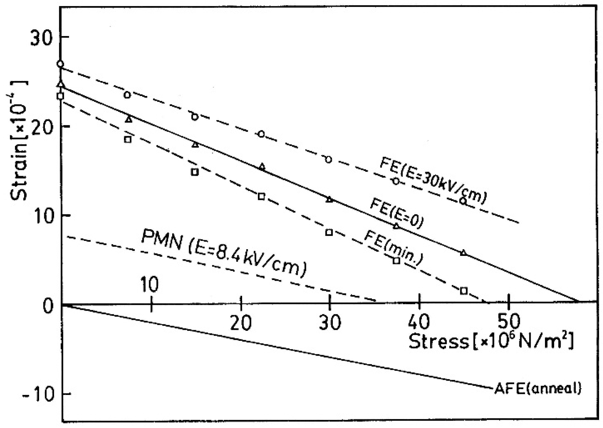
Figure 15 shows the longitudinally induced strains in a shape memory sample of PNZST y = 0.0707 in both the AFE and FE states at room temperature plotted as a function of uniaxial compressive stress for several electric fields [
13]. For comparison, a similar plot for a lead magnesium niobate (PMN) based ceramic (Pb(Mg
1/3Nb
2/3)
0.65Ti
0.35O
3, a well-known electrostrictive material) is also shown.
Roughly speaking, the strain versus stress curve for the AFE PNZST ceramic is shifted along the strain axis with respect to that for PMN due to the difference between the spontaneous strains in the AFE and the FE states. Consequently, the maximum generative force obtained when the ceramic is mechanically clamped so as not to generate a displacement is raised to 80 MPa, in comparison with the normal value for the ferroelectric, 35 MPa in the PMN.
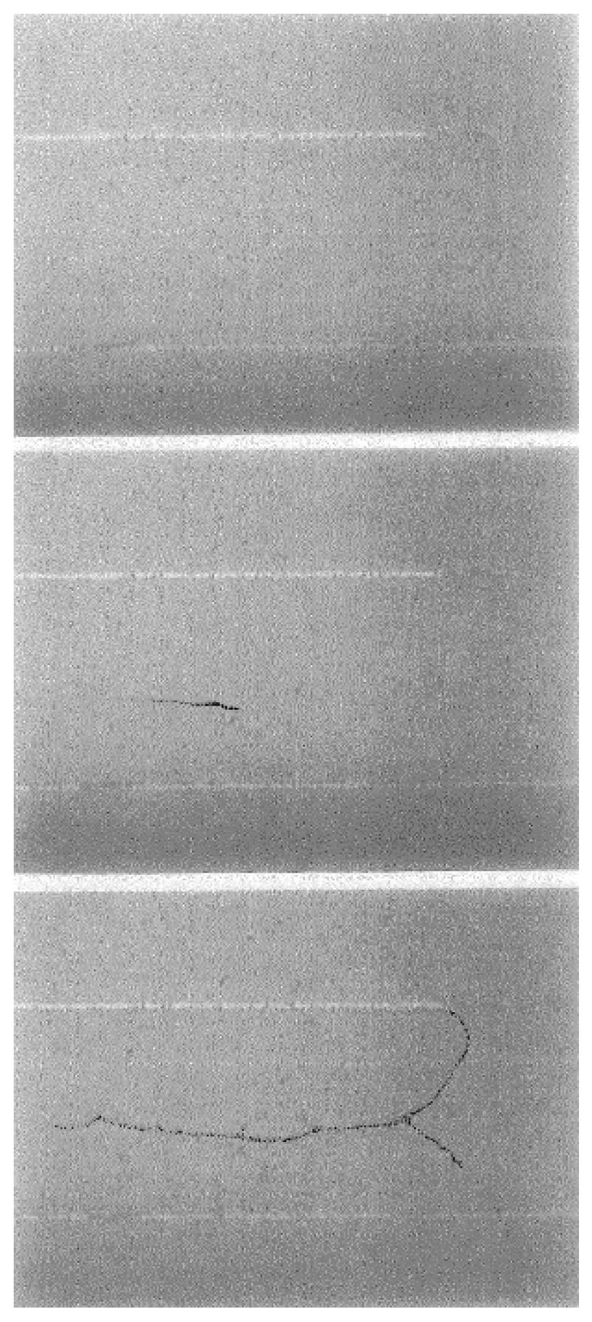
Crack generation and propagation process is very unique in a Pb
0.99Nb
0.02[(Zr
0.6Sn
0.4)
0.955Ti
0.045]
0.98O
3 multilayer (ML) sample, as pictured in
Figure 16 [
18]. As is well-known, the crack is usually initiated around the edge of the internal electrode, then propagates to the ML side-wall in a regular piezoelectric ML sample. However, in the PNZSM ML, the crack is initiated between two electrode layers slightly inside the electrode edge area, propagates in parallel to the electrode layer, then branches into a Y-shape around the electrode edge area. This unique crack propagation mechanism may be originated from the negative Poisson’s ratio or isotropic volumetric expansion associated with the AFE to FE phase transformation. Supposing that the phase transformation starts from the electrode and the phase boundary moves to the center between a pair of the electrodes, large tensile stress is induced around the center area, leading to the crack initiation.
5. Phenomenological Approach
5.1. Electrostrictive Coupling in Antiferroelectrics
We will discuss here the introduction of electrostrictive coupling in Kittel’s free energy expression for antiferroelectrics [
19,
20]. The simplest model for antiferroelectrics is the “one-dimensional two-sublattice model”. It treats the coordinates as one-dimensional, and a superlattice (twice the unit lattice) is formed from two neighboring sublattices each having a sublattice polarization P
a and P
b. The state P
a = P
b represents the ferroelectric phase, while P
a = −P
b, the antiferroelectric phase. For the electrostrictive effect, ignoring the coupling between the two sublattices, the strains from the two sublattices are QP
a2 and QP
b2, respectively (assuming equal electrostrictive constants Q for both sublattices). The total strain of the crystal becomes
However, since antiferroelectricity originates from the coupling between the sublattices, it is appropriate to consider the sublattice coupling also for the electrostrictive effect. The coupling term for the electrostriction Ω was introduced by Uchino
et al. first in the following form [
8,
21]:
in which hydrostatic pressure p was employed, and χ
T is the isothermal compressibility, Q
h (= Q
11 + 2Q
12) and Ω are the electrostrictive constants. Introducing the L. E. Cross’ transformations P
F = (P
a + P
b)/2 and P
A = (P
a − P
b)/2 leads to the following expression:
The dielectric and elastic equations of state follow as
Hence, the induced volume change in the paraelectric phase can be related to the induced ferroelectric polarization by the following formula:
Below the phase transition temperature (this temperature for antiferroelectrics is called
Neel temperature) the spontaneous volume strain and the spontaneous antiferroelectric polarization are related as
Even if the perovskite crystal shows Q
h > 0, the spontaneous volume strain can be positive or negative depending on the value of Ω (Ω < 1 or Ω > 1), that is, if the inter-sublattice coupling is stronger than the intra-sublattice coupling (
i.e., Ω > 1), a volume contraction is observed at the Neel point. This is quite different from ferroelectrics, which always show a volume expansion at the Curie point, such as in BaTiO
3 and PbTiO
3. The large change in the strain associated with the field-induced transition from the antiferroelectric to ferroelectric phase can be estimated to be
Here, we assume that the magnitudes of Pa and Pb do not change drastically through the phase transition; that is, PF,S ≈ PA,S.
Figure 17 illustrates the spontaneous strains in a crystal schematically for Ω > 0 (you may interpret Ω = q
33/Q
33 in the figure). When P
a and P
b are in the parallel configuration (ferroelectric phase), the Ω-term acts to increase the strain x
S, when they are in the anti-parallel configuration (antiferroelctric phase), the Ω-term acts to decrease the strain.
We expand the phenomenology to a three-dimensional formulation [
22]. Considering the simplest case of a tetragonal spontaneous distortion of the primitive perovskite cell, let us start by reducing the 3D polarization (P
1 P
2 P
3) to a simple form (0 0 P
3). The Gibbs elastic free energy is represented by using two-sublattice polarization P
a and P
b, and stress X under a cubical supposition that s
33E = s
11E, s
31E = s
12E,
etc.:
Here, Q
33 and Q
31 denote the conventional longitudinal and transverse electrostrictive coefficients (intrasublattice coupling), and q
33 and q
31 are the corresponding intersublattice coupling parameters (the ratio q/Q was denoted as Ω in the above). Introducing the transformations
leads to four types of stable states under zero applied electric field: nonpolar (P
F3 = P
A3 = 0), polar (P
F3 ≠ 0, P
A3 = 0), antipolar (P
F3 = 0, P
A3 ≠ 0), and semipolar (P
F3 ≠ 0, P
A3 ≠ 0) states. The spontaneous polarization and strains derived from the free-energy function are summarized as follows for the ferroelectric and antiferroelectric and antiferroelectric states:
Here, TC and TN are the Curie and Neel temperatures, respectively, and C is the Curie–Weiss constant. Note again that we presume the cubical symmetry physical parameter components.
5.2. Estimation of q33 and q31
The values of q
33 and q
31 can be obtained from the strain changes associated with the electric-field-induced and thermally induced phase transitions. The spontaneous strains generated at the phase transition from paraelectric to antiferroelectric are described as
The strain changes associated with the field-induced transition from antiferroelectric to ferroelectric are given by
Here we have assumed that P
F3 = P
A3 because only the flipping of polarizations P
a and P
b would occur at the transition. Let us estimate the q
33 and q
31 values using experimental strains and polarization data for Pb
0.99Nb
0.02[(Zr
0.6Sn
0.4)
0.94Ti
0.06]
0.98O
3 (
Figure 6 and
Figure 8a) [
7] and δT
N/δp of the PbZrO
3-based sample [
21]:
Then we derive the followings:
It is noteworthy that q33 and q31 have the same positive sign (accidentally almost the same value), while Q33 and Q31 have the opposite sign with a “piezoelectric Poisson’s” ratio of 1/3.
5.3. Piezoelectric Anisotropy in Antiferroelectrics
Let us derive the piezoelectric coefficients for the ferroelectric state with the sublattice polarization coupling. Under a small external field E applied, the polarization is given by
where ε
3 is the relative permittivity. Using Equations (14) and (15), longitudinal and transversal strains are represented as
The first term describes the spontaneous strains, and
Figure 17 illustrates the spontaneous strain changes due to the sublattice interactions in the case of q
33, q
31 > 0. When the spontaneous polarization P
F3,S exists, the third term (pure electrostriction) is negligibly small in comparison with the second term (piezostriction), and the piezoelectric d coefficients are denoted as
Using the above physical parameters in
Section 5.2 and ε
3 = 600 in
Figure 7, we can evaluate d
31 = 2(Q
31 + q
31)∙ε
0∙ε
3∙P
F3,S = −8 × 10
−12 m/V. This value is close to the experimentally obtained d
31 = −7 × 10
−12 m/V, as shown in
Figure 18, though we use a rough cubic-symmetry approximation such as s
33E = s
11E, s
31E = s
12E,
etc. The “piezoelectric Poisson’s” ratio d
31/d
33 is given by (Q
31 + q
31)/(Q
33 + q
33) and it can differ from the usual value Q
31/Q
33 (≈ −1/3) of the normal ferroelectrics, owing to the values of q
33 and q
31. Using the above values again, we can estimate d
31/d
33= −(1/9).
The electromechanical coupling factors k
t and k
p are represented as
Supposing again that
,
≈ 0.75, and σ ≈ 1/3, we obtain
For the antiferroelectric-based piezoelectrics, taking into account the above discussion, kt/kp will be equal to 4.5, much larger than the normal PZT value around 2.0.
Table 1 lists several anisotropic piezoelectric data for field-biased PNZST’s, PbZrO
3- and PbTiO
3-based ceramics [
23]. The electromechanical coupling factors k
t (thickness mode) and k
p (planar mode) range from 0.5 to 0.6 and 0.05 to 0.15, respectively, and the anisotropy k
t/k
p reaches more than 4.0. In contrast, the ratio k
t/k
p for the intermediate composition of the solid solution Pb(Zr,Ti)O
3 will not exceed 2.5, which is also listed in
Table 1 [
23].
It is important to note that most of the samples exhibiting piezoelectric anisotropy are closely related to antiferroelectricity or sublattice structure. Some of them based on PbZrO
3 are originally antiferroelectric at a low temperature or even at room temperature, and the ferroelectricity is induced after a very high electric field is applied (
i.e., poling process). In Ca-modified PbTiO
3 ceramics [
25], a crystallographic superlattice structure has been observed in the annealed state, which suggests an antiferroelectric sublattice structure. In conclusion, we would remark that even if the sample is not originally antiferroelectric, it seems to possess rather large sublattice dipole coupling.
6. Comparison with Shape Memory Alloys
The phenomenon associated with shape memory alloys is attributed to the stress-induced (as well as thermally-induced) phase transition referred to as “martensitic”. The new strain phenomena in AFE ceramics described here are very easily understandable, if we use the terminology conventionally used for these alloys, replacing electric field E for stress X. The “digital displacement” and the ferroelectric-state memorization discussed here correspond to the “superelasticity” and the shape memory effect in the alloys, respectively.
Outstanding merits of the ceramics over the alloys are:
quick response in ms;
good controllability by electric field to memorize and recover the shape without generating heat;
low energy consumption as low as 1/100 of the alloy; and
wide space is not required to obtain the initial shape deformation.
Numerical comparison among the shape memory alloys and antiferroelectric ceramics is summarized in
Table 2.
7. Applications of Shape Memory Ceramics
The conventional piezoelectric/electrostrictive actuators have been developed with the aim of realizing “analogue displacement transducers”, in which a certain magnitude of electric field corresponds to only one strain state without any hysteresis during rising and falling electric field. This is exemplified by the electrostrictive PMN based ceramics. On the contrary, the antiferroelectrics introduced in this article may be utilized in a device based on a new concept, “a digital displacement transducer”, in which bistable ON and OFF strain states exist for a certain electric field. This idea may be interpreted as a stepping motor in the conventional terminology of electromagnetic motors. The discrete movement through a constant distance achieved by the new actuator is well suited for applications such as an optical-grid manufacturing apparatus or a swing-type charge coupled device.
The shape memory ceramics were applied to devices such as latching relays and mechanical clampers, where the ceramic is capable of maintaining the excited ON state even when electricity is not applied continuously to it.
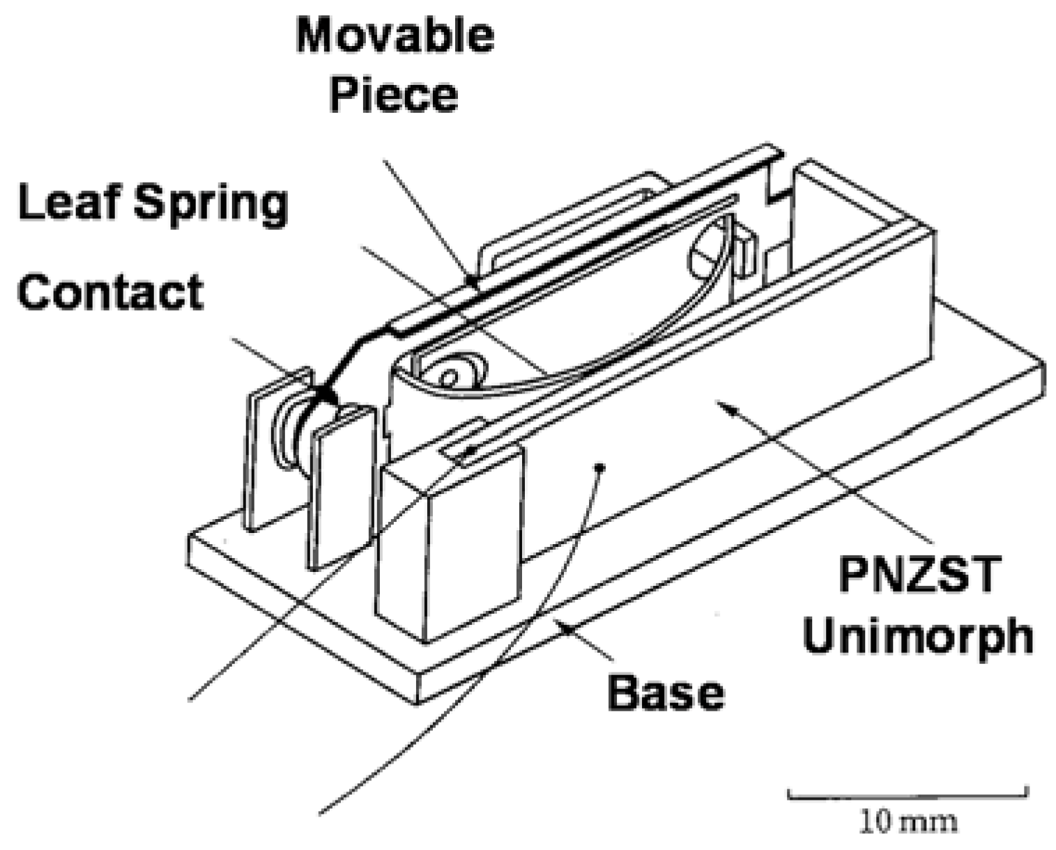
7.1. Latching Relay
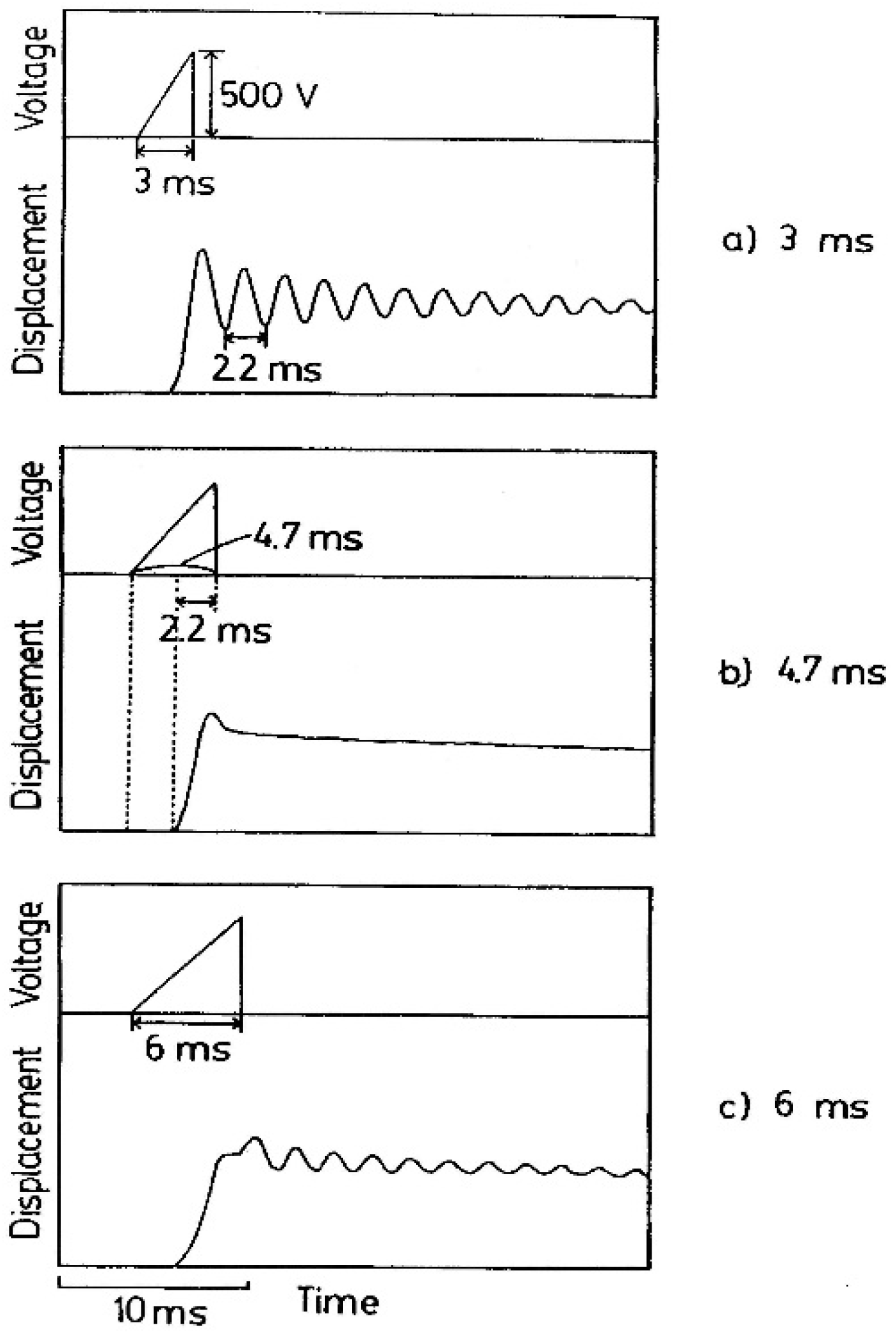
Figure 19 shows the structure of a fabricated latching relay, which is composed essentially of a mechanical snap-action switch and a shape memory unimorph driving part [
27]. The snap-action switch is easily driven by a 50-μm displacement, having mechanically bistable states. The unimorph is fabricated with two y = 0.063 ceramic plates of 22 mm × 7 mm area and 0.2 mm thickness, bonded together with adhesive.
Figure 20 shows the dynamical response of the unimorph. It is noteworthy that the phase transition arises quickly enough to generate the following mechanical resonant vibration (
Figure 20a). When the rise time of the electric field is adjusted to 4.7 ms (
Figure 20b), which is the sum of the mechanical resonance period (2.2 ms) and the lag time to cause the phase transition (2.5 ms), the ringing can be suppressed completely. As shown in
Figure 20c, too slow pulse exhibits again the vibration ringing, which may induce the “chattering” problem in the relay.
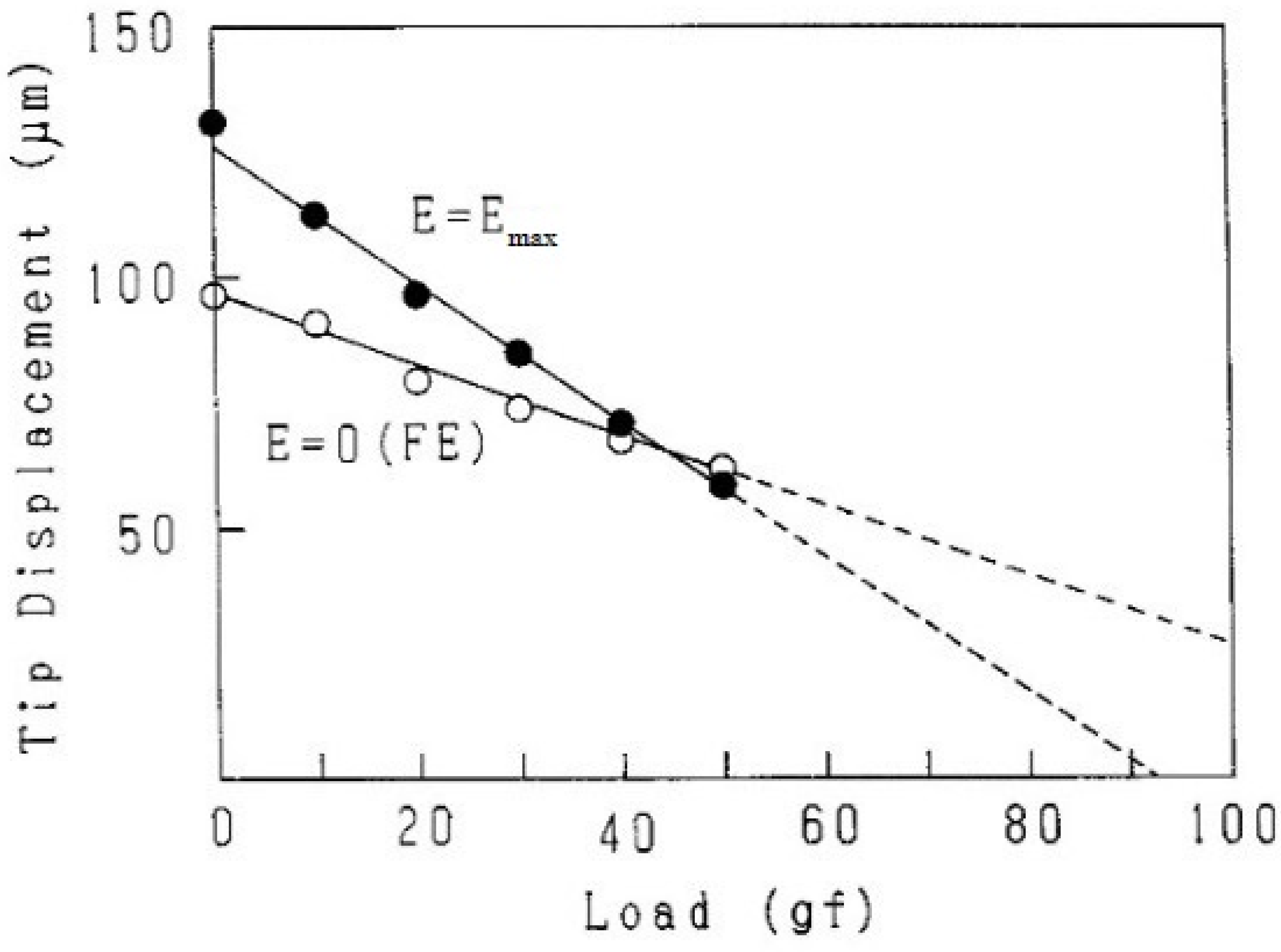
Figure 21 shows the unimorph tip displacement degradation under an external load, which guarantees the 50 μm, minimum displacement to ensure the snap-action, under a couple of tens of gram force, which needs to operate the snap-action switch.
The new relay is very compact in size (20 × 10 × 10 mm
3), 1/10 of a conventional electromagnetic type (20 × 26 × 34 mm
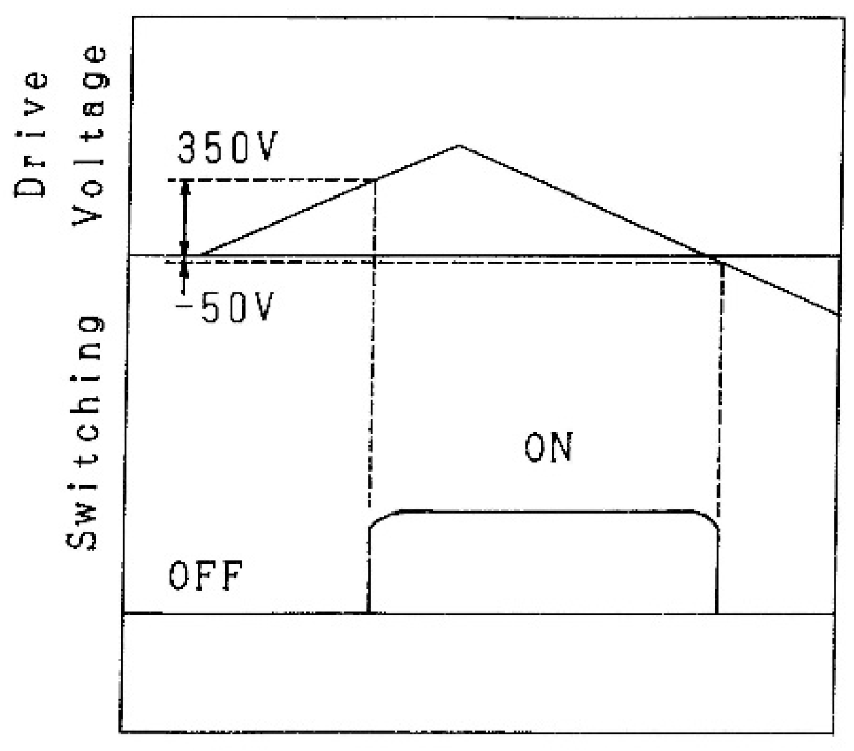
3), and is operated by a pulse voltage, which provides a significant energy saving. The relay is turned ON at 350 V with 4 ms rise time, and turned OFF at −50 V, as depicted in
Figure 22.
Figure 23 demonstrates dynamical response of the latching relays of shape memory ceramic type (
Figure 23a), and a conventional electromagnetic coil type (
Figure 23b). The required duration of the drive voltage 600 V is only 3.4 ms (maximum 10 mA) for the ceramic, while it is 16 ms for the electromagnetic type (
i.e., 1/5 energy saving, compared with the electromagnetic type!). Note also the response time (to realize ON) difference of only 1.8 ms in the ceramic from 8.0 ms in the electromagnetic coil type, which is originated from the actuator response speed (
i.e., electromagnetic actuators are slow!). The existing chattering problem in the antiferroelectric ceramic for 11 ms will be solved technically in the snap-action switch design improvement.
7.2. Mechanical Clamper
A mechanical damper suitable for microscope sample holders has been constructed by combining a 20-layer shape memory stacked device (y = 0.0635) and a hinge-lever mechanism as shown in
Figure 24 [
28]. Application of a 1 ms pulse voltage of 200 V can generate the longitudinal displacement of 4 μm in the 4 mm-thick multilayer device, leading to 30 μm tip movement of the hinge lever after the displacement amplification. Stable grip was verified for more than several hours. This gripper is useful for optical and/or electron microscope sample stages, because no continuous electric voltage application is required during the experiment. To release the sample, small reverse pulse voltage is applied on the multilayer actuator.
8. Summary
Antiferroelectrics (AFE) can exhibit a shape memory function controllable by electric field, with huge isotropic volumetric expansion (0.26%) associated with the AFE to Ferroelectric (FE) phase transformation. Small inverse electric field application can realize the original AFE phase. The response speed is quick (2.5 ms). In the Pb0.99Nb0.02[(Zr0.6Sn0.4)1-yTiy]0.98O3 (PNZST) system, the shape memory function is observed in the intermediate range between high temperature AFE and low temperature FE, or low Ti-concentration AFE and high Ti-concentration FE. In the AFE multilayer actuators (MLAs), the crack is initiated in the center of a pair of internal electrodes under cyclic electric field, rather than the edge area of the internal electrodes in normal piezoelectric MLAs. The two-sublattice polarization coupling model was proposed to explain: (1) isotropic volume expansion during the AFE-FE transformation; and (2) piezoelectric anisotropy. We introduced latching relays and mechanical clampers as possible unique applications of shape memory ceramics.
The study of shape memory antiferroelectric materials was initiated by our group in the 1980s–1990s. Further investigations on the improvement of the induced strain magnitude, the stability of the strain characteristics with respect to temperature change, mechanical strength and durability after repeated driving are required to produce practical and reliable devices. This category of ceramic actuators, as well as piezoelectric/electrostrictive materials, will be a vital new element in the next generation of “micro-mechatronic” or electromechanical actuator devices.


