Article

RDAMS: An Efficient Run-Time Approach for Memory Fault and Hardware Trojans Detection

1
Institute of Microelectronics of Chinese Academy of Sciences, Beijing 100029, China
2
School of Microelectronics, University of Chinese Academy of Sciences, Beijing 100049, China
3
Beijing Key Laboratory of Three-Dimensional and Nanometer Integrated Circuit Design Automation Technology, Beijing 100029, China
*
Author to whom correspondence should be addressed.
Information 2021, 12(4), 169; https://doi.org/10.3390/info12040169
Submission received: 9 March 2021 / Revised: 8 April 2021 / Accepted: 11 April 2021 / Published: 14 April 2021

Abstract

:
Ensuring the security of IoT devices and chips at runtime has become an urgent task as they have been widely used in human life. Embedded memories are vital components of SoC (System on Chip) in these devices. If they are attacked or incur faults at runtime, it will bring huge losses. In this paper, we propose a run-time detection architecture for memory security (RDAMS) to detect memory threats (fault and Hardware Trojans attack). The architecture consists of a Security Detection Core (SDC) that controls and enforces the detection procedure as a “security brain”, and a memory wrapper (MEM_wrapper) which interacts with memory to assist the detection. We also design a low latency response mechanism to solve the SoC performance degradation caused by run-time detection. A block-based multi-granularity detection approach is proposed to render the design flexible and reduce the cost in implementation using the FPGA’s dynamic partial reconfigurable (DPR) technology, which enables online detection mode reconfiguration according to the requirements. Experimental results show that RDAMS can correctly detect and identify 10 modeled memory faults and two types of Hardware Trojans (HTs) attacks without leading a great performance degradation to the system.

1. Introduction

The rapid development of IoT applications has led to the widespread use of IoT devices. People’s life becomes convenient by using IoT devices. McKinsey & Company forecasts that the worldwide number of IoT-connected devices will increase to 43 billion by 2023 [1]. IoT devices widely use system on chip (SoC), and embedded memories occupies more than 50% of the chip area [2]. As the important components of SoC, memories are more prone to fault than other circuit logic due to limitations in design structure, manufacturing technology and production time. Moreover, they hold a large amount of user information and critical data, which increase the risk of them being targets for malicious attacks [3]. The security threats can be software-based attacks occurring at the application of IoT devices, but in recent years, increasing attention has been directed to the potential threat posed by hardware-based attacks [4,5,6]. Once a fault or an attack occurs, it could change the function of the device, leak critical data, even bring loss of property and life to the user [7,8,9,10]. Therefore, detecting security threats in memories has become an urgent task in hardware security.
Nowadays, memory faults are mainly tested by March algorithm [11,12]. The March algorithm has been modified into many improved versions for different test needs, which either improve fault coverage or reduce detection time [13,14]. Most of these works focus on the SoC testing phase. However, faults can also occur during operation due to aging and abrasion of the device. Such faults often disrupt memory read/write functions, making the chip work incorrectly [15].
Most memory attacks are achieved by implanting Hardware Trojans (HTs) [16,17]. HTs are defined as malicious circuits inserted in an electronic system, which enable the adversary to spy confidential contents, destroy kernel functions or denial of service in systems. Researchers have proposed sufficient works to conduct HTs detection for embedded memory before deployment [18]. However, stealthy HTs can be more sophisticated, some are specifically designed to evade pre-deployment detection, to trigger and launch attacks at runtime [6,19]. Thus, efficient memory HTs detection methods in the post-deployment phase should be considered.
Some researchers have proposed methods that detect memory faults and HTs. Tang et al. [15] proposed an online test method for run-time memory faults achieved by BIST (Built-in Self-Test), but the method can only detect faults. De et al. [16] found that Read/Write Followed by Validating Read method can detect a CPU-level system attack of HT, but the method cannot detect other types of HTs. Bolat et al. [17] designed a security protection architecture for microprocessor systems to detect HTs embedded in instruction memory and data memory. The architecture can effectively detect HTs that use malicious software to make the microprocessor run irregular instructions and read/write data in illegal memory areas. Palmiero et al. [20] designed a hardware dynamic information flow tracking (DIFT) architecture for RISC-V processor cores. DIFT supports a policy that detect memory corruption attacks. However, neither of these two architectures can flexibly configure detection mode when facing different detection requirements. Yan et al. [21] proposed a security checking architecture which is applied to the embedded chip for run-time inspection, but the architecture can only detect Stuck-at fault for memory. When memory is being detected, it cannot respond to access requests from the system bus. In addition, the detection mode in the architecture cannot be flexibly updated during runtime. Ray et al. [22] proposed an SoC security architecture that uses a formal verification method to detect hardware threats, and implemented an update of the detection mode during operation. However, the architecture does not specifically perform detection for memory and does not design a diagnostic process to distinguish between memory faults and attacks.
In this paper, we propose a detection architecture for memory security (RDAMS) that can effectively detect both run-time faults and attacks. The kernel function of our architecture is a dedicated, centralized IP block, referred to as SDC (Security Detection Core). It is an FSM-based (Finite State Machine) firmware-upgradable module that realizes memory detection of various modes. Once the SDC detects a memory threat, it will report the problem to system and user, which provides information for further defensive operations. The SDC interfaces with the constituent memory block in a SoC using a “memory wrapper” integrated with the memory. The memory wrapper collects memory state and reports it to the SDC. During detection, memory wrapper assists the SDC in completing the detection. We demonstrate how to use the proposed architecture to detect run-time memory security threat through several memory fault models and memory attack models. Memory detection at runtime can also be achieved by BIST, but to our current knowledge, there is still no BIST technique that can detect both faults and HTs attacks [15,23,24].
Additionally, unlike traditional pre-deployment testing, run-time detection systems could increase the cost in terms of power, area, and resources of the SoC [22,25]. How to reduce the impact of detection towards SoC performance and maintain the original throughput of system is another challenge. Thus, we design a checking mechanism which minimizes the effect of original performance by providing a low latency response to CPU access requests during detection; in order to reduce the cost, we propose a block detection approach and design four detection modes with different granularity. RDAMS is implemented using the FPGA’s dynamic partial reconfigurable (DPR) technology [26,27,28,29], which enables flexible updates of the detection mode during operation and configures suitable a mode according to the detection requirements.
The RDAMS mainly contributes to:
(i).
Extend the March C- algorithm and innovatively present a diagnosis process of the algorithm, which enables the detection of both run-time memory faults and HT attacks.
(ii).
Design a low latency detection control scheme that can handle the memory access collision between regular bus operation and security detection.
(iii).
Propose a block-based memory detection approach and implement four modes with different detection granularity. Users can flexibly configure the most applicable memory detection mode online according to their detection requirements.
The remainder of this paper is organized as follows. Section 2 introduces fault and attack models for RDAMS. Section 3 presents the design of RDAMS, including: detection algorithm, diagnosis process and detection architecture. Section 4 presents the optimization of RDAMS, including: processing of access collision and Multi-granularity detection mode. The results are discussed in Section 5. We conclude the paper and describe future works in Section 6.

2. Fault and Attack Models

2.1. Fault Models

Based on the functional behaviors, the memory faults can be classified into various types. Table 1 introduces the types of faults that frequently occur in memory [14].

2.2. Attack Models

The memory Hardware Trojan is a redundant circuit maliciously implanted by an attacker, including a trigger and a payload circuit [9]. Once the trigger circuit is activated, the payload circuit will launch a certain attack. Therefore, unlike memory faults that always perform fault behavior, memory Hardware Trojan attacks are episodic in nature and are only launched when the trigger conditions are met.
In the application of the IoTs, a typical scenario is that the sensing device encrypts the collected data and stores it into the memory. If there is an HT in the memory, and the HT is triggered at this time, it will damage the normal function of the device and interfere with the user’s use of the device.
We refer to [30,31,32] to design highly concealed Hardware Trojan circuit. Huang et al. [30,31] designs a HT attacking the functional integrity of AES when AES is running. Once the HT is triggered, the encrypted result of the AES will be a fault. Kanet al. [32] proposes an HT attacking the availability of memory during memory is working. Once the HT is triggered, the memory will not output data.
In this paper, we design two types of memory HTs: HT1 for functional integrity destruction and HT2 for availability disruption. Figure 1 depicts how HT1 and HT2 are triggered and attacked. As shown, the trigger circuits of the two HTs are the same (①), the payload circuit of HT1 is ②, and the payload circuit of HT2 is ③.
The trigger circuit consists of a judgment circuit and a Trojan enable counter (TEC). When the data D and address A meet certain requirements (The second part of A and the fifth and sixth parts of D are both 1), the judgment circuit outputs a counting enable (CntEn) and the TEC starts counting. Once the TEC counts to a threshold, such as 10 or 50, the threshold can be determined by the user. the Trojan enable signal (TjEn) is output to activate the payload circuit. Then, TEC returns to initial value, and the TjEn is pulled down, waiting for the next trigger.
HT1 payload circuit: The payload circuit of HT1 performs an XOR operation on the last part of D and TjEn. In this way, D is tampered and HT1 destroys the functional integrity of memory.
HT2 payload circuit: The payload circuit of HT2 performs an XOR operation on the write enable signal (Write_en) and TjEn. In this way, D cannot be written to memory and HT2 destroys memory availability.

3. Design of RDAMS

We introduce the RDAMS into three aspects. (1) we introduce the detection algorithm of the RDAMS–March C- algorithm. (2) we propose the diagnosis process for distinguishing memory run-time faults and HTs attacks. (3) we describe the architecture of the RDAMS in detail, and focus on the internal implementation details of MDM and MEM_wrapper.

3.1. Detection Algorithm

The RDAMS use March C- algorithm to detect memory. By implementing March C- algorithm in a form of a finite state machine (FSM) and adding the flag register for identification, the RDAMS can detect and identify memory faults listed in Table 1.
Nowadays, there are many detection algorithms to detect memory fault, such as Memory Scan (MSCAN), Checkboard, Galloping Pattern (GALPAT) and March algorithm. March algorithm has strong scalability, according to the fault types, its verification and traversal methods can be changed. Therefore, the March algorithm has many versions, such as MATS, MATS+, MATS++, March A, March C- etc. [12,14,15]. Table 2 lists the fault coverage (FC) and time complexity Ω(n) of the various memory testing algorithms introduced above, where “A” is fully supported, “P” is partially supported, and “N” is not supported. As can be seen from the Table 2, March C- algorithm has superior performance, such as lower time complexity and higher fault coverage [13]. Therefore, we choose March C-algorithm as the detection algorithm of RDAMS.
The testing process of the March C- algorithm is as follows.
①↑(w0); ②↑(r0,w1); ③↑(r1,w0); ④↓(r0,w1); ⑤↓(r1,w0); ⑥↓(r0);
In the process, “w” stands for write operation; “r” stands for read operation. “w0” means write 0 to memory cell; “w1” means write 1 to memory cell; “r0” means read 0 from memory cell; “r1” means read 1 from memory cell. “↑” means operate from low address to high address; “↓” means operate from high address to low address.
RDAMS use FSM to implement the March C- algorithm. In order to identify memory faults, the architecture collects the testing results of each step of the March C- algorithm and stores them in the flag register. Where “1” means read data is in error, “0” means read data is right. After the six testing steps of the March C- algorithm are completed, the RDAMS compares the testing result with the standard result listed in Table 3. If it is the same as the standard result of a certain type of fault, it proves that there is such a memory fault in the memory. Table 3 lists the testing results of the ten types of faults in Table 1.
SAF0 cannot be distinguished from TF 0→1, CFid(↑,0) and CFid(↓,0), because their testing results are the same. For some other faults, like read/write logic fault, neighborhood pattern sensitive fault (NPSF), etc., RDAMS can detect but cannot identify it, because there is no specific testing result corresponding to them.

3.2. Diagnosis Process

The RDAMS use the March C- algorithm and diagnosis process to detect and identify memory faults and HTs at runtime. The detection range for the RDAMS is:
(a)
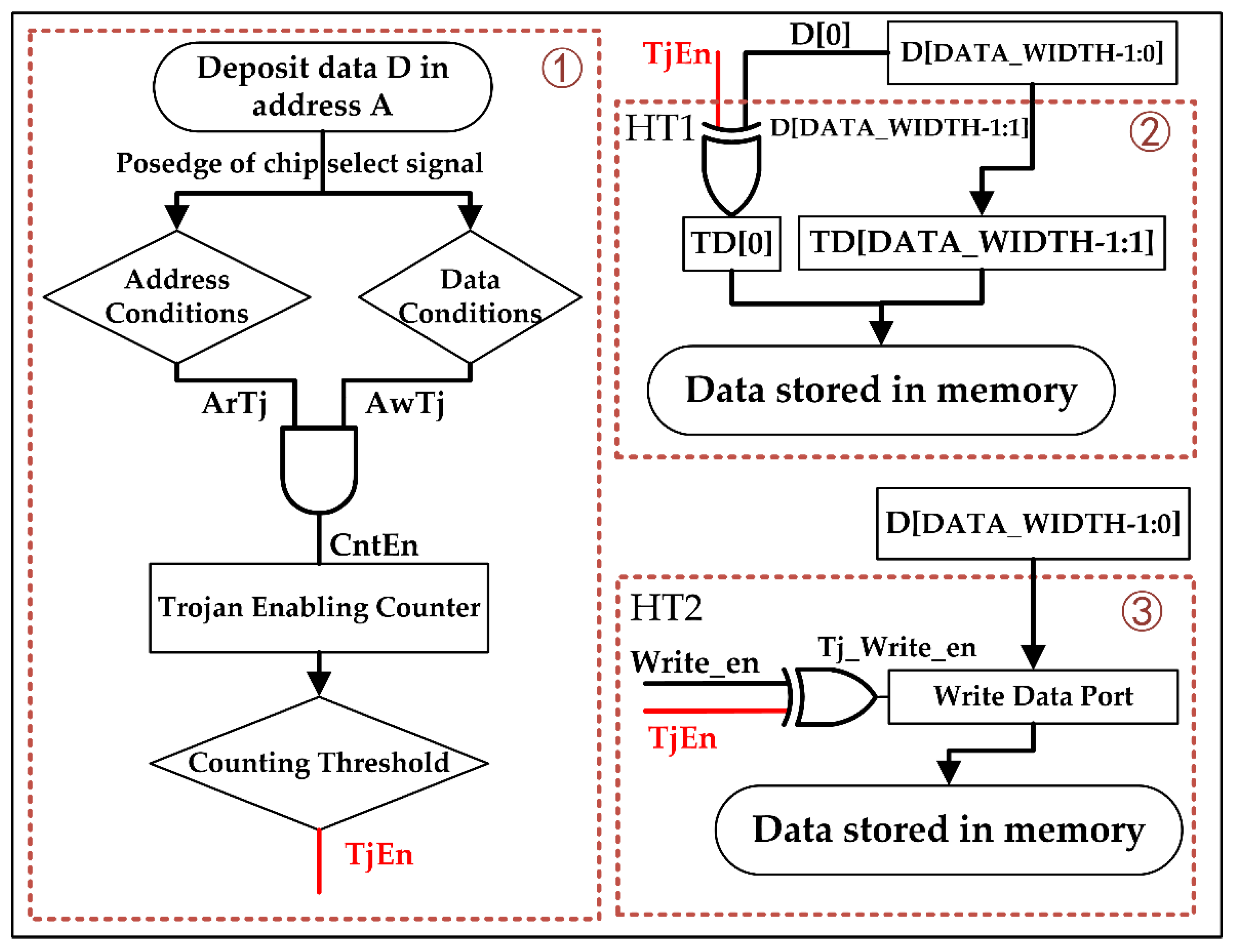
We limit the potential HTs types in memory into functional integrity destruction and availability disruption only (HT1 and HT2). Because they have covered the most typical types of the run-time attack, others involving information leaking can be prohibited by designing a side channel-resisted circuit [33].
(b)
The memory faults that RDAMS can detect and identify are limited to the ten types of faults in Table 1. For some other faults, RDAMS can also detect but cannot identify it.
In order to make the RDAMS available to detect memory attacks, we innovatively design a diagnosis process which enriches a more accurate identification of faults and attacks by analyzing the two rounds detection results of RDAMS operation. Before introducing the diagnosis process, it is important to list the rational assumptions in the architecture.
  • Each potential fault and HT1 in memory only affects one part in each cell (32 bit), HT2 affects 32 parts in each cell. The case that one cell has multiple bits with faults is not considered.
  • Fault and HTs will not appear in the same cell at the same time.
  • HTs attacks are episodic, so HT will not be triggered at the same cell in two consecutive detections.
Figure 2 shows the diagnostic process of the RDAMS for both malicious attacks and faults. For a 32 bit-wide cell, once a security threat is alerted, the results of this and the next round of detection are collected to provide a diagnosis of the kind of security threat. The following is a description of the diagnostic process for each type of memory security threat.
Detectable Faults: In the first round of detection, If the result equals the standard result of the ten types of memory faults introduced in Table 1, we can determine that the memory threat existing in the cell is a memory fault, and identify the type of the fault.
HT2: In the first round of detection, if more than a single bit error is found in the cell, we can infer that the threat is the attack-HT2 due to assumption 1.
Undetectable Faults: Because memory faults are not episodic, there will be a 1-bit error in the result of the first round of detection; in the second round, there will also be a 1-bit error in the same position, but March C- algorithm cannot identify the fault because the result does not equal the standard result listed in Table 3. So, we can only determine that the memory threat existing in the cell is a memory fault.
HT1: For HT1, if in the first round of detection, there is a 1-bit error in the cell, while in the second round of detection, the error does not happen in the cell due to assumption 3. We can determine that the memory threat existing in the cell is HT1.
If in the first round of detection, we detect a memory threat in the cell due to HT1, and in the second round, a memory fault just happens in the same cell at this moment, the process will incorrectly conclude that there is a threat to memory fault. In other words, there will be a misjudgment under this situation. However, the runtime memory fault should occur just at the time gap between the first and second detection procedures. The probability of this scenario occurring is too low to be considered in our architecture.

3.3. Detection Architecture

The RDAMS designs a generic control flow that enables the detection of both memory faults and HTs attacks. Figure 3 shows an overall figure of the RDAMS in an embedded SoC. The detection architecture mainly contains two parts: SDC (Security Detection Core) and MEM_wrapper.
The functions of SDC and MEM_wrapper are as follows:
SDC: The Core that secures the SoC controls and enforces the detection of memory. The SDC can update the detection mode (in Section 4) using DPR technology through the Detection Mode Configuration Port based on the Off-chip Trigger Signal input by the user to perform different modes of detection. Memory State Sense collects the status of Memory and reminds SDC to initiate detection when Memory is found to be idle. Memory Detection Module (MDM) that is implemented by an FSM executes the detection based on the March C- algorithm. It initiates detection after receiving the Detect Enable signal and writes the detection result to Error Log Reg after detection is finished.
MEM_wrapper: Memory is wrapped by MEM_wrapper. MEM_wrapper is controlled by SDC and assists SDC to complete the detection. MEM_wrapper collects the status of Memory and reports it to SDC. Before SDC tests Memory, MEM_wrapper assists SDC to back up the detected memory cell; after SDC tests Memory, MEM_wrapper assists SDC to writes the backed-up data back to cell. During testing, MEM_wrapper receives control signals from SDC, detection signals from SDC, and access signals from bus, and sends detection signals or access signals to memory according to whether there is an access collision (introduced in Section 4). If no detection is running, MEM_wrapper will input the memory access signal from the system bus into the memory.
Figure 4 shows the workflow of the RDAMS performing memory detection. When the user inputs an off-chip trigger signal, the RDAMS configures the corresponding detection mode. Then, when the MEM_wrapper finds that the memory is idle, it will report it to SDC; the SDC starts to back up the detected cell and initiate testing. After testing is finished, the backed-up data are written back to memory cells. After one round of detection, the timer starts timing and initiates the next round of detection when a user-defined time threshold is reached, such as 10 min or 30 min or others. In this period, if an off-chip trigger signal is activated, the RDAMS will update the detection mode and execute another detection.

3.3.1. MDM

MDM is an FSM-based firmware-upgradable module that realizes memory detection of various mode. Figure 5 shows the FSM of MDM, the FSM jumps to different detection phase according to memory state. When the FSM completes one circle, one round of detection is realized. These states mean:
(1)
IDLE: Waiting for enabling detection;
(2)
COPY_MEM & WRITE_REG: Copy the memory cells under detection into MEM_wrapper’s back up registers;
(3)
UP_W0→DOWN_R0: From UP_W0 to DOWN_R0, Executing the March C- algorithm to test memory;
(4)
RECOPY_REG &WRITE_MEM: Write the value of MEM_wrapper’s register back to the detected cell.
(5)
ERROR_LOG: Write the detection results to Error Log Reg.
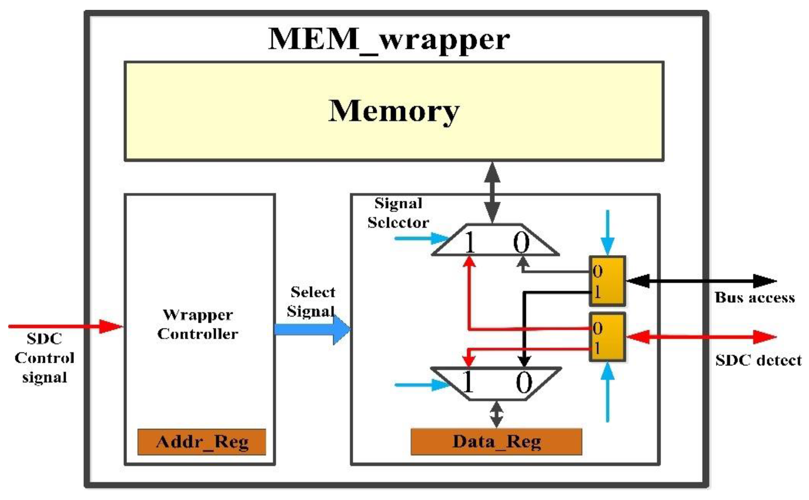
3.3.2. MEM_Wrapper

MEM_wrapper is controlled by SDC and assists SDC to detect memory. It contains two parts, Wrapper Controller and Signal Selector as shown in Figure 6. The Wrapper Controller consists of a state machine for outputting Select Signal based on the SDC control signal and its own state, and registers set (Addr_Reg) storing the address of the detected cells. The Signal Selector consists of a select circuit for selecting the bus access signal or SDC detect signal to memory or Data_Reg based on the Select Signal, and registers set (Data_Reg) storing the data of the detected cells.

4. Optimization of RDAMS

4.1. Processing of Access Collision

During detection, the detection signal will occupy the channel for accessing memory, causing the system signal to temporarily fail to access the memory, thereby delaying the memory access speed of the system and reducing the efficiency and performance of the SoC. In order to reduce the impact of detection on SoC performance and maintain the original efficiency of system, the RDAMS designs a processing of access collision. An access collision is defined as the CPU (or other masters) trying to access an unbacked up memory cell under testing phase, which causes a confliction between detect operation and bus requirement. When there is an access collision, RDAMS can stop detection in a short time and switch to response the access request from the bus.
Because of the processing of access collision, RDAMS will not degrade SoC performance too much. The Algorithm 1 shows the detail of processing of access collision during all phases of detection. The detection contains four phases: Backup, Testing, Write Back, Error Log.
Algorithm 1. Processing of Access Collision.
1:Backup phase.
2:   if bus access memory then
3:     The access is processed in testing phase. end if
4: Testing phase.
5:    if bus accessmemory then
6:   if axi_addr_i = Addr_Reg[i] then
7:      Bus access Data_Reg[i] and testing continues.
8:   else
9:      Record testing status, testing pause and bus access memory.
10:     if bus accessing is over then
11:      Testing continues. end if
12:   end if
13:   else
14:     testing continues.
15:   end if
16: Write Back phase.
17:   if bus access memory then
18:   The access is processed in Error log phase end if
19:  Error Log phase.
20:    Log detection result and process bus access.
In the Backup phase, SDC writes the address of the detected cell into Addr_Reg of MEM_wrapper, and writes the data of detected cell into Data_Reg of MEM_wrapper. If bus has access to memory, the access is deferred to the Testing phase.
In the Testing phase, SDC sends a test signal to memory based on the March C- algorithm. If bus has access to memory, the MEM_wrapper will determine whether the bus access address is equal to the address saved in Addr_Reg. If it is equal, there will not be an access collision, MEM_wrapper will let the bus access Data_Reg, and the test signal is sent to memory at the same time. If it is not equal, there will be an access collision, MEM_wrapper will inform the SDC and SDC will stop the testing, then MEM_wrapper lets the bus access memory; until the bus access is finished, SDC continues the testing.
In the Write Back phase, SDC writes the data saved in Data_Reg back to the corresponding cell. The proposed approach backs up and writes back the data of the targeted cell before and after the Testing phase, respectively, which ensures the correctness and availability of the data in the memory after the Testing phase is finished. If the bus has access to memory, the access is deferred to the Error Log phase.
In the Error Log phase, the detection result is written to Error Log Reg. The testing is finished, so bus access signal is sent to memory.
The timeline of access collision processing in every phase is depicted in Figure 7. TCA is the time of bus accessing; TS is the time when SDC stores the detection state before bus accesses memory; TE is the time when SDC restarts the detecting. In the entire timeline, RDAMS provides five bus accessing modes. including:
Access 1: Before the detection starts (IDLE), the bus access Access 1 is processed without delay, and the processing time of Access 1 is TCA.
Access 2: In the Backup phase, if the bus access Access 2 arrives, it will be processed until the Testing phase. Since Access 2 occurs an access collision (the access address of Access 2 is not equal to the address in Addr_Reg), the detection needs to be suspended; once the bus accessing is finished, the detection continues; the processing time of Access 2 is TS + TCA + TE.
Access 3: The bus access Access 3 arrives in the Testing phase. Since Access 3 does not occur an access collision, the processing time of Access 3 is TCA, which can be executed in parallel with the detection.
Access 4: The bus access Access 4 arrives in the Testing phase. Since Access 4 incurs an access collision, the detection needs to be suspended; once the bus accessing is finished, the detection continues; the processing time of Access 2 is TS + TCA + TE.
Access 5: In the Write Back phase, if a bus access Access 5 arrives it will be processed until the Error Log phase. There is no need to consider whether there is an access collision, because all data have been written back to memory cell in the Write back phase. The processing time of Access 5 is TCA.
Compared with the processing bus access after detection is completed, the processing of access collision has a low influence towards the performance of system. It can be seen from Figure 7 that the performance degradation occurs due to two reasons: (1) Bus accesses the memory in the Backup or Write back phase, then the access is processed until the Testing phase or Error Log phase; (2) Access collision occurs in the Testing phase, then the access is processed until the detection is suspended. In other situations, detection does not degrade the performance. Therefore, RDAMS can maintain the original efficiency of system to some extent.

4.2. Multi-Granularity Detection Mode

4.2.1. The Meaning of Multi-Granularity Detection

In order to make the detection architecture scalable for memories in different depths and further reduce the cost of power and area, we propose a block-based sampling approach. Firstly, memory cells are grouped as fixed size blocks. In each group, four modes are available with different sampling rates (or called detection granularity) for the tester to select and replace in runtime based on current constraints or detection requirements. Figure 8 shows an example of the mentioned approach, in which one group has eight cells, and the four modes are defined as:
  • Mode 1: Randomly select one cell to detect in each group. If no security threat is reported in result, all eight cells are considered secure.
  • Mode 2: Randomly select two cells to detect in each group. If no security threat is reported in result, all eight cells are considered secure.
  • Mode 3: Randomly select four cells to detect in each group. If no security threat is reported in result, all eight cells are considered secure.
  • Mode 4: All eight cells are detected in each group. If no security threat is reported in result, all eight cells are considered secure.
It should be noted that although the example uses eight as the base number for each mode, the number is modifiable. We suggest using power-of-2 as the base number.

4.2.2. Cost Analysis for Multi-Granularity Detection

Different detection modes have different impacts on the cost of the architecture. We analyze these impacts from a qualitative or quantitative perspective on three aspects—resource cost, detection time cost, detection coverage.
Resource cost: Based on the presented approach, the more detected cells are picked out, the more register should be used to back up, so from mode 1 to mode 4, the resource cost near-linearly increases.
Detection time cost: The detection time in this section does not include the pause time when the architecture is processing an access collision. It is the sum of time to execute a round of detection. The time (T) consists of three parts— T b w represents the time of backing up, writing back and logging results, T m represents the time of executing testing and T t r represents the time of changing state in the SDC.
T = T b w + T m + T t r
The detection time T of mode 1, mode 2, mode 3 and mode 4 are set as T 1 ,   T 2 ,   T 3 and T 4 , respectively. The time for one cell to be backed up, written back, and logged is t c , and the time for one cell to be tested by algorithm is t m , and the switching time of mode 1, mode 2, mode 3 and mode 4 are T t r 1 , T t r 2 , T t r 3 and T t r 4 , respectively.
T 1 = t c + t m + T t r 1
T 2 = 2 ( t c +   t m ) + T t r 2
T 3 = 4 ( t c +   t m ) + T t r 3
T 4 = 8 ( t c +   t m ) + T t r 4
When T t r is small, T 1 , T 2 ,   T 3 and T 4   are roughly linear. As the number of detected cells in a group increases, the detection time T increases.
Detection coverage: The detection coverage C is the ratio of the detected cells to all memory cells. The value is related to the number of detected cells in one group. The detection coverage C of mode 1, mode 2, mode 3 and mode 4 are 0.125, 0.25, 0.5 and 1. It should be noted that since mode 1 only chooses one cell to detect in one group, it cannot detect coupling faults.

5. Results and Discussion

To validate the RDAMS, we design the fault and attack module by Verilog HDL, and implant them in the architecture. The RDAMS with fault and attack modules has been functionally verified by Modelsim SE-64 10.4. We discuss the impact of RDAMS to the SoC performance based on synthesis and implementation results from vivado 2019. The overall RDAMS along with the fault and attack models are implemented on an experimental test-bed environment which contains a field programmable gate array (FPGA, XC7Z020-CLG484) [34], static random access memory (SRAM) and various interfaces.

5.1. Fault Detection Results

The detected memory depth is 36 and the width is 32 bit. The address space is 32′H40000000–32′H4000008c. Table 4 list the address and the position of fault model implanted in the memory.
Figure 9 shows the detection result by Modelsim SE-64 10.4. The “STCC” means the fault may be SAF0, TF 0→ 1, CFid (↑, 0), or CFid (↓, 0). The “CFinD” means the fault is CFin (↓,↕). The “CFidD1” means the fault is CFid (↓, 1). According to the result and the diagnosis process proposed above, the architecture can correctly identify the type of faults in Table 4. This indicates the RDAMS can accurately detect and identify memory faults listed in Table 1.

5.2. Attack Detection Results

According to the assumption 3 in Section 3.2, the memory attacks (HT1 and HT2) will not be triggered at the same cell in two consecutive detections. Figure 10 shows the two rounds detection result of HT1. In the first round, the security threats occurred at 4 and 22; in the second round, the security threats occurred at 14 and 20. The cells that had security threats in the first round do not have security threats in the second round, according to the diagnosis process and detection range, we can determine that the hardware Trojan is HT1.
Similar to HT1, Figure 11 shows the two rounds detection result of HT2. According to the diagnosis process, we can determine that the Hardware Trojan is HT2 just by the result of the first-round detection.

5.3. Verification on FPGA

We implanted memory faults and HT attacks into the RDAMS, respectively, and used Vivado SDK to sending write and read signals to the memory in order to verify whether the faults and HT attacks acted as designed. Figure 12 shows that the RDAMS reads and writes to the memory implanted with SAF0 and SAF1.
In Figure 12, the memory cell whose address is 32′H40000004 is implanted with SAF0. After writing 32’Hffffffff to the memory cell, the data read out are 32’Hfffffffe. The memory cell whose address is 32′H40000010 is implanted with SAF1. After writing 32’H00000000 to the memory cell, the data read out are 32’H00000001.
Figure 13 is a picture of the RDAMS implanted with SAF0 and SAF1 performing detection. There are two LEDs on the board. The bottom one indicates that the detection has been completed, and the top one indicates that listed security threats have been detected. We performed the similar tests with the ten types of faults in Table 1, and attacks of HT1 and HT2. The results show that RDAMS can correctly detect faults and HTs attack models.

5.4. Verification of Access Collision Processing

Figure 14 shows the Processing of access collision. The red signal is the SDC detect signal; the purple signal is the bus access signal, and the green signal is input to memory. During the memory testing, the CPU wants to write 32′h20202020 to the eighth cell. At the same time, the SDC detection signal wants to read the second cell. Because RDAMS prioritizes the execution of bus accesses, the memory testing is suspended. When the bus access is finished, the testing is turned on and RDAMS lets SDC read the second cell.
Table 5 shows the delay time of processing bus access in the testing phase. In testing, if there is no access collision, the bus access can be processed timely; if there is an access collision and the request is a write operation, the request can be processed without latency, but RDAMS needs two clocks to turn on testing after the request is processed completely; if the request is a read operation, the request will be processed after one clock, and RDAMS needs two clocks to turn on testing after the request is processed completely.
According to the analysis in Section 4.1 and the experimental results listed in Table 5, we can learn that the architecture performance is related to the number of cells detected in a group. If there are fewer detected cells in a time, there will be more collisions in the testing phase; if we increase the number of detected cells, the probability of collision will be reduced, but the backup and write back phase time will be longer, and it may lead to more bus accessing delay in the testing phase. Moreover, the areas and resource cost will also rise with the increase in detected cells. Therefore, the number of detected cells should have an optimal solution n1, which has the least impact on the performance.

5.5. Cost of Detection Architecture

The resource cost and the time to perform a round of detection on the memory with a depth of 36 for four modes are shown in Table 6. From mode 1 to mode 4, the cost increases. The results prove the correctness of the prediction of resource cost in Section 4.2.2. In the absence of access collisions, from mode 1 to mode 4, the detection time increases, which basically conforms to the mathematical model constructed in Section 4.2.2.

6. Conclusions

In this paper, we propose an architecture, RDAMS, to efficiently detect runtime threats in embedded memory circuits by:
(i).
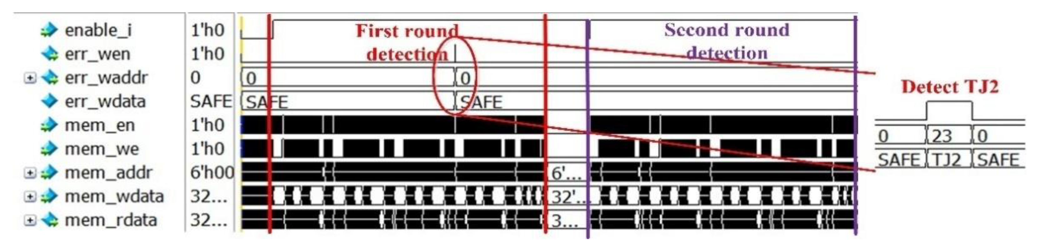
The RDAMS can correctly detect and identify all the ten types of memory faults listed in Table 1 and two types of HTs triggered at runtime—HT1 (for functional integrity), HT2 (for availability). The diagnosis process ensures that the architecture can detect faults after one round of detection, and diagnose HTs attacks after two rounds of detection.
(ii).
The RDAMS is designed with a collision handling mechanism which enables a lower latency response to bus access requests during detection (For read requests: TS = 1 clock, TE = 2 clock; for write requests: TS = 0 clock, TE = 2 clock).
(iii).
The block-based sampling approach and DPR-based implementation make the architecture scalable for different memories and online reconfigurable for detection modes, which occupies fewer resources.
The future work will focus on two aspects. One is to optimize the memory detection algorithm to cover more faults and attack models; the other is to design an automatic tool for RDAMS, so that users can conveniently implant it in their own SoC in IoT devices and configure suitable detection content.

Author Contributions

Conceptualization, J.W. and Y.L.; methodology, J.W.; validation, J.W.; formal analysis, J.W.; investigation, J.W.; resources, J.W.; data curation, J.W.; writing—original draft preparation, J.W.; writing—review and editing, J.W. and Y.L.; supervision, Y.L.; funding acquisition, Y.L. All authors have read and agreed to the published version of the manuscript.

Funding

This research was funded by the National Key R&D Program of China (2019YFB2102400).

Institutional Review Board Statement

Not applicable.

Informed Consent Statement

Not applicable.

Data Availability Statement

The data presented in this study are available on request from the corresponding author. The data are not publicly available due to privacy or ethical.

Acknowledgments

The first author, J.W., hereby acknowledges the Institute of Microelectronics of the Chinese Academy of Sciences (IMECAS) and the EDA Center.

Conflicts of Interest

The authors declare no conflict of interest.

References

  1. Dahlqvist, F.; Patel, M.; Rajko, A.; Shulman, J. Growing Opportunities in the Internet of Things. Available online: https://www.mckinsey.com/industries/private-equity-and-principal-investors/our-insights/growing-opportunities-in-the-internet-of-things (accessed on 2 March 2021).
  2. SEMICO Research Corporation. Available online: http://www.semico.com (accessed on 18 February 2021).
  3. Saeidi, R.; Garakani, H.G. SRAM hardware Trojan. In Proceedings of the 2016 8th International Symposium on Telecommunications (IST), Tehran, Iran, 27–28 September 2016; pp. 719–722. [Google Scholar]
  4. Suwansrikham, P.; Kun, S.; Hayat, S.; Jackson, J. Dew Computing and Asymmetric Security Framework for Big Data File Sharing. Information 2020, 11, 303. [Google Scholar] [CrossRef]
  5. Hamad, M.; Prevelakis, V. SAVTA: A Hybrid Vehicular Threat Model: Overview and Case Study. Information 2020, 11, 273. [Google Scholar] [CrossRef]
  6. Kim, L.; Villasenor, J.D. Dynamic Function Verification for System on Chip Security Against Hardware-Based Attacks. IEEE Trans. Reliab. 2015, 64, 1229–1242. [Google Scholar] [CrossRef]
  7. Das, B.; Das, N.; Sikdar, B.K. Effect of Trojans on Write Data Access in Memory. In Proceedings of the 2019 9th International Symposium on Embedded Computing and System Design (ISED), Kollam, India, 13–14 December 2019; pp. 1–5. [Google Scholar]
  8. Khan, M.N.I.; De, A.; Ghosh, S. Cache-Out: Leaking Cache Memory Using Hardware Trojan. IEEE Trans. Very Large Scale Integr. (VLSI) Syst. 2020, 28, 1461–1470. [Google Scholar] [CrossRef]
  9. Jianfeng, Z.; Gang, S. A Survey on the studies of Hardware Trojan. J. Cyber Secur. 2017, 2, 74–90. [Google Scholar]
  10. Koshy, T.; Arun, C.S. Diagnostic data detection of faults in RAM using different march algorithms with BIST scheme. In Proceedings of the 2016 International Conference on Emerging Technological Trends (ICETT), Kollam, India, 21–22 October 2016; pp. 1–6. [Google Scholar]
  11. Die, H.; Junmin, W. A Parallel Memory Fault Detection Scheme Combined with Hardware Characteristic. Comput. Eng. 2014, 40, 310–314. [Google Scholar]
  12. Tong, Z.; Benmao, C.; Xiaofeng, Z. Design of BIST Testing SRAM Based on MARCH Algorithm. Comput. Mod. 2013, 1, 99–101. [Google Scholar]
  13. Jun, X.; Lan, W.; Jinlong, G.; Dan, C.; Zenghua, F. Design of memory detection for raising reliability of vital computer. Railw. Comput. Appl. 2014, 23, 47–52. [Google Scholar]
  14. Ailing, R.; Ming, L.; Guanglin, W.; Rui, L. An Efficient Diagnosis Algorithm for the Test of Embedded SRAM. J. Appl. Sci. 2005, 2, 178–182. [Google Scholar]
  15. Zhenkun, T. An Online Self-Healing Research Based on ECC and BISR for Embedded RAM. Master’s Thesis, University of Electronic Science and Technology of China, Chendu, China, 2020. [Google Scholar]
  16. De, A.; Nasim Imtiaz Khan, M.; Nagarajan, K.; Ghosh, S. HarTBleed: Using Hardware Trojans for Data Leakage Exploits. IEEE Trans. Very Large Scale Integr. (VLSI) Syst. 2020, 28, 968–979. [Google Scholar] [CrossRef]
  17. Bolat, A.; Cassano, L.; Reviriego, P.; Ergin, O.; Ottavi, M. A Microprocessor Protection Architecture against Hardware Trojans in Memories. In Proceedings of the 2020 15th Design & Technology of Integrated Systems in Nanoscale Era (DTIS), Marrakech, Morocco, 1–3 April 2020; pp. 1–6. [Google Scholar]
  18. Xiongwei, L.; Xiaohan, W.; Yang, Z.; Kaiyan, C.; Lu, X. Survey on the Hardware Trojan Protection. J. Ordnance Eng. Coll. 2015, 27, 40–50. [Google Scholar]
  19. Hoque, T.; Wang, X.; Basak, A.; Karam, R.; Bhunia, S. Hardware Trojan attacks in embedded memory. In Proceedings of the 2018 IEEE 36th VLSI Test Symposium (VTS), San Francisco, CA, USA, 22–25 April 2018; pp. 1–6. [Google Scholar]
  20. Palmiero, C.; Guglielmo, G.D.; Lavagno, L.; Carloni, L.P. Design and Implementation of a Dynamic Information Flow Tracking Architecture to Secure a RISC-V Core for IoT Applications. In Proceedings of the 2018 IEEE High Performance extreme Computing Conference (HPEC), Greater Boston, MA, USA, 25–27 September 2018; pp. 1–7. [Google Scholar]
  21. Huayu, Y.; Lan, C.; Xin, T.; Ying, L. Design of SoC Security Check Architecture for Internet of Things Applications. Comput. Eng. 2021, 47, 152–159. [Google Scholar]
  22. Basak, A.; Bhunia, S.; Ray, S. A flexible architecture for systematic implementation of SoC security policies. In Proceedings of the 2015 IEEE/ACM International Conference on Computer-Aided Design (ICCAD), Austin, TX, USA, 2–6 November 2015; pp. 536–543. [Google Scholar]
  23. Libo, Z.; Wei, T.; Wei, Y.; Junling, L. Full-Speed Test Design Based on Memory Built-in Self-Test. Microelectron. Comput. 2018, 35, 43–46. [Google Scholar]
  24. Dongming, C.; Jianbing, C.; Zhikuang, C. MBIST Design for the 40 nm SoC Chip. Chin. J. Electron Devices 2017, 40, 813–818. [Google Scholar]
  25. Basak, A.; Bhunia, S.; Ray, S. Exploiting design-for-debug for flexible SoC security architecture. In Proceedings of the 2016 53nd ACM/EDAC/IEEE Design Automation Conference (DAC), Austin, TX, USA, 5–9 June 2016; pp. 1–6. [Google Scholar]
  26. Xilinx. Vivado Design Suite User Guide: Partial Reconfiguration. Available online: https://www.xilinx.com/support/documentation/sw_manuals/xilinx2018_2/ug909-vivado-partial-reconfiguration.pdf (accessed on 20 May 2020).
  27. Xilinx. Partial Reconfiguration Controller v1.3: LogiCORE IP Product Guide. Available online: https://www.xilinx.com/support/documentation/ip_documentation/prc/v1_0/pg193-partial-reconfiguration-controller.pdf (accessed on 26 May 2020).
  28. Nath, A.P.D.; Bhunia, S.; Ray, S. ArtiFact: Architecture and CAD Flow for Efficient Formal Verification of SoC Security Policies. In Proceedings of the 2018 IEEE Computer Society Annual Symposium on VLSI (ISVLSI), Hong Kong, China, 8–11 July 2018; pp. 411–416. [Google Scholar]
  29. Nath, A.P.D.; Ray, S.; Basak, A.; Bhunia, S. System-on-chip security architecture and CAD framework for hardware patch. In Proceedings of the 2018 23rd Asia and South Pacific Design Automation Conference (ASP-DAC), Jeju Island, Korea, 22–25 January 2018; pp. 733–738. [Google Scholar]
  30. Zhe, H. Design and Detection of Hardware Trojan Horse. Master’s Thesis, South China University of Technology, Taipei, Taiwan, 2016. [Google Scholar]
  31. Huang, Z.; Yao, R.; Luo, F. Trigger Circuit of Hardware Trojan Based on Up/Down Counter. IEICE Trans. Electron. 2015, 98, 279–282. [Google Scholar] [CrossRef]
  32. Kan, S.; Dworak, J. Triggering Trojans in SRAM circuits with X-propagation. In Proceedings of the 2014 IEEE International Symposium on Defect and Fault Tolerance in VLSI and Nanotechnology Systems (DFT), Amsterdam, The Netherlands, 1–3 October 2014; pp. 1–8. [Google Scholar]
  33. Fang, X.; Luo, P.; Fei, Y.; Leeser, M. Balance power leakage to fight against side-channel analysis at gate level in FPGAs. In Proceedings of the 2015 IEEE 26th International Conference on Application-specific Systems, Architectures and Processors (ASAP), Jeju, Korea, 27–29 July 2015; pp. 154–155. [Google Scholar]
  34. Crockett, L.H.; Elliot, R.; Enderwitz, M.; Stewart, R. The Zynq Book: Embedded Processing with the ARM Cortex-A9 on the Xilinx Zynq-7000 All Programmable SoC; Strathclyde Academic Media: Glasgow, Scotland, 2014. [Google Scholar]
Figure 1. Hardware Trojan (HT)1 and HT2’s triggering and attack methods.
Information 12 00169 g001
Figure 2. The diagnostic process.
Information 12 00169 g002
Figure 3. The overall figure of the run-time detection architecture for memory security (RDAMS).
Information 12 00169 g003
Figure 4. The workflow of the RDAMS.
Information 12 00169 g004
Figure 5. The finite state machine for Memory Detection Module (MDM).
Information 12 00169 g005
Figure 6. The structure of MEM_wrapper.
Information 12 00169 g006
Figure 7. The timeline of access collision processing.
Information 12 00169 g007
Figure 8. Four Detection Modes.
Information 12 00169 g008
Figure 9. Detection Result for Faults.
Information 12 00169 g009
Figure 10. Detection result for HT1.
Information 12 00169 g010
Figure 11. Detection result for HT2.
Information 12 00169 g011
Figure 12. Read result of RDAMS implanted with stuck at fault (SAF)0 and SAF1.
Information 12 00169 g012
Figure 13. RDAMS performing detection.
Information 12 00169 g013
Figure 14. Processing of access collision.
Information 12 00169 g014
Table 1. Ten types of memory faults.
TypeNameBehavior
Stuck at Fault (SAF)SAF 0The value of cell is stuck at 0
SAF 1The value of cell is stuck at 1
Transition Fault (TF)TF 0→1The value of cell cannot transition from 0 to 1
TF 1→0The value of cell cannot transition from 1 to 0
Inversion Coupling Fault (CFin)CFin(↑, ↕) 1When writing a cell, the value of another cell is inverted
CFin(↓, ↕) 2
Idempotent Coupling Fault (CFid)CFid(↑, 0) 3When writing a cell, the value of another cell is fixed at 0
CFid(↓, 0)
CFid(↑, 1) 4When writing a cell, the value of another cell is fixed at 1
CFid(↓, 1)
1 ↑ means the address of the written cell is higher than the address of the inverted/fixed cell. ↕ means invert. 2 ↓ means the address of the written cell is lower than the address of the inverted/fixed cell. 3 0 means the fixed cell is fixed to 0. 4 1 means the fixed cell is fixed to 1.
Table 2. Performance comparison of memory testing algorithms.
AlgorithmΩ(n)SAFTFCFinCFid
MATS4nNNNN
MATS+5nANNN
MATS++6nAANN
March A15nAAAA
March C-10nAAAA
MSCAN4nANNN
GALPAT4 n 2 AAAA
Table 3. Standard testing results of the fault model.
Fault↑(w0)↑(r0,w1)↑(r1,w0)↓(r0,w1)↓(r1,w0)↓(r0)Results
SAF000101001010
SAF101010110101
TF 0→100101001010
TF 1→000010100101
CFin(↑,↕)01101011010
CFin(↓,↕)01101111011
CFid(↑,0)00101001010
CFid(↑,1)01010010100
CFid(↓,0)00101001010
CFid(↓,1)01000110001
No Fault00000000000
Some Other Fault01/01/01/01/01/0Other
Table 4. Fault model implanted in memory.
Fault ModelAddressDepth
SAF032′H400000041
SAF132′H400000104
TF 0 → 132′H4000002810
TF 1 → 032′H4000003413
CFin (↓,↕)32′H4000005020
CFid (↓,1)32′H4000005822
Table 5. The delay time of processing bus access in testing phase.
Collision (Yes/No)Request(W/R)TS (/clk:100 MHz)TE (/clk:100 MHz)
YesW02
R12
Table 6. The time and resource cost for four detection mode.
ModeResource CostTime (/clk: 100 MHz)
SlicesLUTFF
Mode 1147448164243
Mode 2174532208453
Mode 3222624292869
Mode 42817764401545
Publisher’s Note: MDPI stays neutral with regard to jurisdictional claims in published maps and institutional affiliations.

