Article

Absorption by a Layered Microbolometer Pixel’s Active Element

by
Christos Bolakis
* and
Christos N. Vazouras
*
Division of Battle Systems, Naval Operations, Sea Studies, Navigation, Electronics and Telecommunications, Hellenic Naval Academy, Hadjikyriakou Ave., 18539 Piraeus, Greece
*
Authors to whom correspondence should be addressed.
Computation 2024, 12(5), 108; https://doi.org/10.3390/computation12050108
Submission received: 30 April 2024 / Revised: 14 May 2024 / Accepted: 15 May 2024 / Published: 20 May 2024

Abstract

:
Microbolometer arrays, i.e., arrays of micro-scale pixels sensing temperature via resistance changes, have proven to be an effective basis for real-time imaging instrumentation in infrared as well as terahertz frequencies. In previous work, a design of THz and IR absorbing nano-laminates of dielectric and metal layers was studied. It was shown via numerical modeling that absorption may be maximized by appropriate choices of thickness, permittivity and conductivity. In this work, an analytical approach to the problem is formulated based on the standard recursive multiple reflection formulas for multi-layered planar structures. The results fully confirm and extend previous numerical work. A previous relationship between wavelength and silicon thickness for maximum absorption, derived numerically for specific parameter combinations, is now generalized in a parametric closed form. The method can be extended to include multiple lossy dielectric layers and may serve as a tool for optimizing the absorption characteristics of more complex layered absorbing structures. This could enhance the sensitivity of the detection scheme of interest, providing benefits in terms of cost, efficiency, precision, and adjustability.

1. Introduction

A lot of research focuses on the absorption of electromagnetic (EM) waves, pertaining to a vast variety of applications, from military systems, e.g., in the reduction of Radar Cross Section (RCS) [1], to medical imaging [2,3] and more. More particularly, thermal imaging is used in a wide range of applications, especially in security and military environments. Microbolometer arrays—comprising micro-scale pixels whose resistance is highly sensitive to changing temperatures—have proven to be an effective class of sensors for real-time infrared imaging systems [4]. A significant potential for innovative applications exists, e.g., the use of microbolometer cameras has been recently proposed [5] for observation of outgoing longwave radiation at the Earth Climate Observatory space mission. In such sensors, the radiation absorbed by a thermal detector causes its pixel’s temperature to rise, and that specific rise can be detected using a temperature-sensitive element. According to the main principle of thermal detection mechanism, the wavelength response of thermal detector is determined by the infrared absorbing material. With the proper choice of absorber, an appropriate response of the thermal detectors may be achieved for wavelengths of interest. Because this technology is based upon temperature-driven changes in pixel resistivity, produced by the absorption of incident EM radiation (rather than electron-hole generation/recombination, as is the case for most semiconductor-based photodetectors), such devices are not susceptible to thermal excitation and can be routinely operated at room temperature [6]. Furthermore, the relatively short thermal time constant (~10 ms) of the microbolometer focal plane array (FPA) allows real-time imaging at frame rates comparable to TV monitors (~30 Hz). Nearly all such cameras are designed and engineered for use in the infrared regime (typically 8–14 μm).
Under normal operation in the infrared regime, gray body radiation—originating from objects within the camera’s field of view—falls upon the FPA; the distinct thermal response resulting in each pixel allows for the generation of images which are essentially gray body intensity maps of the scene before the camera. For example, human body detection is easily achieved, since the core temperature is typically ~10 K above room temperature (~300 K) and the Noise Equivalent Temperature Difference (NETD) of most microbolometers is less than 0.1 K in the infrared regime [6].
Recent work has focused on enhancing the absorption capability of microbolometer pixel elements. An interesting study [7] explores the potential of using black silicon as an alternative anti-reflection layer for uncooled infrared cameras based on microbolometers. Typically, these cameras employ silicon caps with anti-reflection coatings to minimize Fresnel reflection losses and maintain a vacuum inside the bolometer array.
In a related context, numerous studies have explored advances in materials and the development of uncooled infrared microbolometer devices. A recent comprehensive review [8] includes materials such as α-Si, VOx, and novel materials like carbon nanotubes (CNTs) and TiO2−x due to their significant potential to improve the temperature coefficient of resistance (TCR) and reduce noise in device performance. The evolution from traditional materials to advanced nanostructures seeks to enhance the performance metrics of microbolometers operating at room temperature. Notably, α-Si microbolometers can achieve TCR values around −3%/K, which can be further enhanced to −4.5%/K with boron doping [9]. Gold–black phosphorus nanostructured absorbers for efficient light trapping in the mid-infrared region show promising TCR values and high responsivity [10]. Furthermore, non-stoichiometric TiO2−x thin films are highlighted for their high TCR values (−2.56%/K) and low 1/f noise, indicating their potential to replace traditional materials in future microbolometer applications [11]. These advancements reflect a significant shift towards optimizing uncooled microbolometers for broader and more effective applications in fields requiring thermal imaging.
In this paper, a simple analytical approach is presented to optimize absorption from layered structures (a glass layer adjacent to a thin metallic layer) for use in microbolometer sensors. The optimization of structures of this type has been studied numerically in previous work [12,13] for the THz and infrared (IR) frequency regions. Based on the present approach, previous numerical results are confirmed and generalized in closed-form expressions. More specifically, a simple closed-form expression for the optimal thickness of the dielectric layer to maximize absorption, valid for any combination of materials, is derived; its results are found to match very well (as a special case) the results of a linear equation derived in previous work by numerical interpolation for a specific set of materials. Thus, the present method appears to be suitable for the application of optimization procedures for various design parameters, reducing computation time and complexity as compared with fully numerical techniques; it also seems amenable to an extension to more complex multilayered structures.

2. System Model and Analytical Optimization Approach

2.1. Absorber Setup

In previous work [12,13] an effective double-layered absorber consisting of a metal and a glass layer showed promising results regarding integration into a microbolometer. Through the usage of such a metal–glass configuration, the transmittance ( T ) of a metal film is the same, regardless of the direction in which it is measured (from the metal side or the glass side). This is not the case for reflectance ( R ), which is lower when measured at the glass side than at the metal side. Since T + R + A = 1 , the reduction in reflectance at the glass side means that the absorptance ( A ) from that side must be higher [12]. Additionally, modifying the process to replace the glass layer with a material that has a higher temperature coefficient of resistance (TCR) could further enhance performance. This improvement comes from both the metal and the dielectric being sensitive to temperature changes, rather than just the metal.
The absorber studied in this paper is designed as a thin layer of metal located on a high TCR material (diluted poly-Si). The schematic is illustrated in Figure 1.
The absorption of electromagnetic radiation in a thin metal film located on a poly-Si medium can be calculated via transmission and reflection coefficients, taking into account multiple reflections at each interface of the double-layered absorber, as illustrated in Figure 2 and explicitly described in [12,14]. The absorption coefficient is then estimated by subtracting transmission and reflection coefficients from 1.
For the results shown below, we assume a poly-Si (diluted form) layer with a refractive index of 5.2 (e.g., [15]). The frequency-dependent refractive index of the metal thin film is given [16,17] by
n = ( 1 j ) σ 4 π ε 0 f  
where f is the frequency of incident radiation and σ is the metal film conductivity, which determines its absorptive behavior. As is well known, a critical wavelength (corresponding to the plasma frequency) exists, below which the metal becomes transparent to incident radiation. Notably, Equation (1) is valid because the shortest wavelength in our analysis is the lowest limit of the long wavelength infrared (LWIR) region (3 to 5 μm), namely 3 μm, and well above the plasma wavelengths of metals of interest (see, e.g., [18]).

2.2. A Generalized Analytical Solution

The overall reflection and transmission coefficients for the multi-layered structure may be determined based on multiple reflections at each interface. The absorption is then estimated by subtracting reflection from the unity, since the transmission from medium 3 (metal) is considered to be 0. For the simplification of formulas and ease of comparison with previous results, two assumptions were made here: first, the metal layer is 100% absorptive (and hence treated as an infinite conducting half-space), and second, the dielectric layer is lossless. However, the validity of the approach does not depend on these assumptions; the same analysis may be pursued generally for a finite metal layer of finite conductivity, as well as for a lossy dielectric layer (or any number of such layers). In future work, the analysis will be extended for more complex multi-layered structures of interest. As will be shown in the following, the “wide-spectrum linear equation” found previously, i.e., Equation (10), below, is recovered as a special case of the generalized formula derived by this approach.
We denote by r i j and t i j the reflection and transmission coefficients, respectively, at the interface between mediums i and j, as shown in Figure 3, given by the well-known relations
r i j = γ i γ j γ i + γ j ,     t i j = 1 r i j  
The overall reflection ( r ) and transmission ( t ) coefficients are r = E ( r ) / E ( i ) and t = E ( t ) / E ( i ) , respectively. Based on the standard procedure for wave reflection and transmission at multiple layer interfaces as described in [17], these coefficients are
r = r 12 + r 23 e 2 γ 2 d 2 1 + r 12 r 23 e 2 γ 2 d 2  
and
t = ( 1 + r 12 ) t 32 e 2 γ 2 d 2 1 + r 12 r 23 e 2 γ 2 d 2  
where d 2 is the thickness of layer 2 and γ 2 = j 2 π f μ 0 ε 2 = α 2 + j β 2 is the complex propagation constant, with μ 0 and ε 2 as the magnetic permeability (same for all media) and the complex dielectric constant of medium 2. For a lossless dielectric, we have
β = 2 π c f   ,     c = 1 μ 0 ε 0 ε r
where ε r is the dielectric constant and c is the velocity of electromagnetic waves in the medium of interest.
The overall power reflection coefficient of the structure, i.e., the fraction of the incoming power reflected from medium 2 into medium 1 of Figure 3, is | r | 2 = r r * , and the overall power transmission coefficient, i.e., the fraction of the incoming power transmitted from medium 2 into medium 3 of Figure 3, is | t | 2 = t t * . Based on realistic parameter values and the results illustrated in the following section, we may assume that the dielectric layer (medium 2) is effectively lossless ( a 2 d 2 1 e a 2 d 2 1 ) and the metal layer (medium 3) absorbs all power transmitted into it ( e a 3 d 3 1 0 ). Under these assumptions, to maximize absorption by the metal layer, | r | 2 should be minimized, or (equivalently) | t | 2 should be maximized, which can be expressed as
| t | 2 = t t * | t 21 | 2 | t 32 | 2 1 + | r | 2 + 2 | r | cos ( 2 β 2 d 2 φ )  
where
r = r 12 r 23 = | r | exp ( j φ )
For any given choice of material for medium 2, optimizing | t | 2 can be achieved by varying the thickness d 2 . From (5), it may be seen that | t | 2 is maximized for
cos ( 2 β 2 d 2 φ ) = 1
Obviously, (7) has infinite solutions
2 β 2 d 2 = φ + ( 2 n + 1 ) π
Since medium 1 is air, medium 2 is dielectric and medium 3 is metal, it follows from (3) that the phase coefficients of both r 12 and r 23 will be between π / 2 and π , and hence from (6) we conclude that π φ 2 π . To keep the overall dimensions compact, the preferred solution is the one yielding a minimum thickness d 2 , which corresponds to the choice of n = −1 in (8), namely
2 β 2 d 2 , o p t = φ π
and hence
d 2 , o p t = φ π λ 2 4 λ 2 4  
where λ 2 is the wavelength in medium 2 and φ is the phase of r , as in (6) above. Thus, d 2 , o p t is the optimal thickness, corresponding to maximum absorption for the three-layer configuration illustrated in Figure 3.

3. Results and Comparison with Numerical Optimization Approach

3.1. Numerical Optimization Procedure

According to previous experimental results, presented in [12], the absorber was initially adjusted at the frequency of 6 THz, and consisted of a glass layer (BK 7) with 4.9 μm thickness and a refractive index of 2.52, on top of a thin metal film of sheet resistance of 55 [Ohm/square]. The absorption achieved was up to 86%. Taking advantage of the fact that after increasing the refractive index of the dielectric medium, a respective increase in the absorption occurred, the glass layer was substituted with a material of high refractive index (diluted poly-Si with n = 5.2 ) and a numerical fine-tuning process was carried out [13] by the repeated computation of reflection and transmission coefficients for varying thickness values via finite element modeling. As an example of the process, nearly 100% absorption was achieved at a frequency of 6 THz under normal incidence. Based on the findings for the THz spectrum [12], using the same numerical procedure, absorption optimization was also demonstrated in [13] in both the mid and the long wavelength infrared spectra from 3 to 14 μm, resulting in the design of a double-layered poly-Si absorber for use as the active pixel element of a microbolometer, with the ability to absorb approximately 96% and reflect less than 1% of the incident power over a wide frequency spectrum.

3.2. Numerical Calculation of the Optimized Absorber Parameters

Using the numerical optimization procedure in [13], the design of a double-layered absorber with optimized absorptance characteristics at any frequency of interest across the THz or IR spectrum was achieved, as illustrated with a specific example (optimized at 6 THz) in Figure 4.
For a double-layered absorber consisting of a poly-Si layer with a refractive index of 5.2 and a metal layer of a 15 [Ohm/square] sheet resistance, repeating the numerical optimization for four distinct wavelengths in the THz spectrum from 2.5 to 10 THz and in both mid- and long-wavelength infrared regions (MWIR and LWIR, respectively), the results given in Table 1 and Table 2 were computed [13].
Table 1 and Table 2 suggest a linear relationship between poly-Si (medium 2) thickness and resonant frequency (wavelength). The linearity is depicted in Figure 5.
Using linear regression fitting, we can obtain a “wide-spectrum linear equation” [13] for the appropriate thickness of the poly-Si medium for any wavelength of interest, encompassing both the THz (2.5–10 THz) and IR (3–14 μm) spectra, as follows:
d 2 , o p t [ μ m ] = 0.048 λ 2 [ μ m ] 0.017
where λ 2 is the wavelength of interest in the dielectric medium (medium 2 above) and d 2 , o p t is the optimizing thickness of the poly-Si layer.
We note that Equation (10) has been derived numerically by linear regression, based on results from the previously developed numerical technique via finite element modeling, independently from Equation (9), and is valid for the specific set of materials of the double-layered absorber described above (poly-Si layer with a refractive index of 5.2 and a metal thin layer of a 15 [Ohm/square] sheet resistance). But a linear relationship between silicon thickness and wavelength is reasonable in a more general sense, based on the fact that the silicon thickness directly influences the effective optical path and, consequently, the phase shift experienced by the incident electromagnetic wave. As the thickness of the silicon layer increases, the optical path that these waves traverse within the medium also increases. This alteration in path length affects the interference patterns within the layered structure, which are crucial for determining the resonant absorption peaks [16]. Similar behavior is also exhibited by the more general Equation (9) derived here.
As a further example, the poly-Si layer thickness maximizing absorption at wavelengths of 11 and 4 μm (i.e., the center of LWIR and MWIR spectral regions) was calculated using (10), and the corresponding absorption behavior is illustrated in Figure 6.
For a comparison of the analytical technique proposed here with the numerical approach developed previously, the optimal thickness value was calculated by means of the generalized Equation (9) of the present analytical approach for the absorber setup of interest (Figure 2) and the wavelengths corresponding to spectral regions of MWIR (3–5 μm) and LWIR (8–14 μm). For the set of materials shown in Table 1, the results are shown in Figure 7, along with results calculated using the previously found “wide-spectrum linear Equation (10)”; the results are almost identical. Thus, the previous Equation (10), derived numerically for a specific choice of materials for media 2 and 3, is shown to be in close agreement with Equation (9), which generalizes the result for any choice of materials.

4. Conclusions

In this paper, a design and optimization technique for a double-layered absorber of a thin metal layer located on a poly-Si medium is presented. This type of element appears to be a promising candidate for integration into microbolometer sensors. As illustrated, the sensing element can be used in broadband applications, since absorption may be optimized across the THz spectrum (2.5–10 THz) and both the mid and the long wavelength IR regions (3–14 μm). A relationship between silicon thickness and maximum absorption frequency, previously derived numerically for specific dielectric parameter combinations, is now generalized in a parametric closed form. This allows for the significant acceleration of the design calculations for any combination of materials and parameters. The extension of the method to more complex layered structures is envisaged for future work, to explore additional optimization opportunities afforded by integrating additional layers onto the microbolometer element. The optimization of multi-layered structures is expected to further increase the sensitivity of the detection scheme, as well as improve the adjustability, offering advantages in terms of cost, efficiency and precision.

Author Contributions

Conceptualization, C.B. and C.N.V.; Data curation, C.B.; Formal analysis, C.B. and C.N.V.; Investigation, C.B.; Methodology, C.B. and C.N.V.; Validation, C.N.V.; Visualization, C.B.; Writing—original draft, C.B.; Writing—review and editing, C.N.V. All authors have read and agreed to the published version of the manuscript.

Funding

This research received no external funding.

Data Availability Statement

The original contributions presented in the study are included in the article, further inquiries can be directed to the corresponding authors.

Conflicts of Interest

The authors declare no conflict of interest.

References

  1. Lynch, D. Introduction to RF Stealth; SciTech Publishing: Raleigh, NC, USA, 2004. [Google Scholar]
  2. Brun, M.-A.; Formanek, F.; Yasuda, A.; Sekine, M.; Ando, N.; Eishii, Y. Terahertz imaging applied to cancer diagnosis. Phys. Med. Biol. 2010, 55, 4615–4623. [Google Scholar] [CrossRef] [PubMed]
  3. Ashworth, P.C.; Pickwell-MacPherson, E.; Provenzano, E.; Pinder, S.E.; Purushotham, A.D.; Pepper, M.; Wallace, V.P. Terahertz pulsed spectroscopy of freshly excised human breast cancer. Opt. Express 2009, 17, 12444–12454. [Google Scholar] [CrossRef] [PubMed]
  4. Kruse, P.W. Uncooled Thermal Imaging: Arrays, Systems, and Applications; SPIE Press: Bellingham, WA, USA, 2002. [Google Scholar]
  5. Dewitte, S.; Abdul Nazar, A.A.; Zhang, Y.; Smeesters, L. A Multispectral Camera Suite for the Observation of Earth’s Outgoing Radiative Energy. Remote Sens. 2023, 15, 5487. [Google Scholar] [CrossRef]
  6. López-Alonso, J.M. Noise Equivalent Temperature Difference (NETD). In Encyclopedia of Optical and Photonic Engineering, 2nd ed.; CRC Press: Boca Raton, FL, USA, 2016; pp. 1766–1773. [Google Scholar]
  7. Bardalen, E.; Bouchouri, A.; Akram, M.N.; Nguyen, H.-V. Black Silicon as Anti-Reflective Structure for Infrared Imaging Applications. Nanomaterials 2024, 14, 20. [Google Scholar] [CrossRef] [PubMed]
  8. Yadav, P.V.K.; Yadav, I.; Ajitha, B.; Rajasekar, A.; Gupta, S.; Reddy, Y.A.K. Advancements of Uncooled Infrared Microbolometer Materials: A Review. Sens. Actuators A Phys. 2022, 342, 113611. [Google Scholar] [CrossRef]
  9. Shin, C.; Pham, D.P.; Park, J.; Kim, S.; Lee, Y.-J.; Yi, J. Structure and electrical properties of boron doped hydrogenated mixed-phase silicon films for uncooled microbolometer. Infrared Phys. Technol. 2018, 96, 84–88. [Google Scholar] [CrossRef]
  10. Audhkhasi, R.; Povinelli, M.L. Gold-black phosphorus nanostructured absorbers for efficient light trapping in the mid-infrared. Opt. Express 2020, 28, 19562–19570. [Google Scholar] [CrossRef] [PubMed]
  11. Yadav, I.; Jain, S.; Joshi, S.R.; Goyal, A.; Tomar, M.; Gupta, S.; Dutta, S.; Chatterjee, R. Compositional, electrical and thermal properties of nonstoichiometric titanium oxide thin films for MEMS bolometer applications. Mater. Sci. Semicond. Process. 2022, 148, 106779. [Google Scholar] [CrossRef]
  12. Bolakis, C.; Karanasiou, I.S.; Grbovic, D.; Karunasiri, G.; Uzunoglu, N. Optimizing detection methods for terahertz bio imaging applications. Opt. Eng. 2015, 54, 067107. [Google Scholar] [CrossRef]
  13. Bolakis, C.; Karanasiou, I.S.; Grbovic, D.; Vazouras, C.; Karunasiri, G.; Uzunoglu, N. Optimizing the Absorption Capability of a Microbolometer Pixel’s Active Element. Int. J. Electromagn. Appl. 2019, 9, 1–6. [Google Scholar]
  14. Lecaruyer, P.; Maillart, E.; Canva, M.; Rolland, J. Generalization of the Rouard method to an absorbing thin-film stack and application to surface plasmon resonance. Appl. Opt. 2006, 45, 8419–8423. [Google Scholar] [CrossRef] [PubMed]
  15. Müllerová, J.; Jurečka, S.; Šutta, P. Optical characterization of polysilicon thin films for solar applications. Sol. Energy 2006, 80, 667–674. [Google Scholar] [CrossRef]
  16. Born, M.; Wolf, E.; Bhatia, A.B.; Clemmow, P.C.; Gabor, D.; Stokes, A.R.; Taylor, A.M.; Wayman, P.A.; Wilcock, W.L. Principles of Optics, 7th ed.; Cambridge University Press: Cambridge, UK, 1999. [Google Scholar]
  17. Balanis, C. Advanced Engineering Electromagnetics, 2nd ed.; Wiley: Ney York, NY, USA, 2012. [Google Scholar]
  18. Feynman, R. The Feynman Lectures on Physics. new millennium, Ed.; California Institute of Technology: Pasadena, CA, USA, 2010; Volume 2, pp. 3211–3213. [Google Scholar]
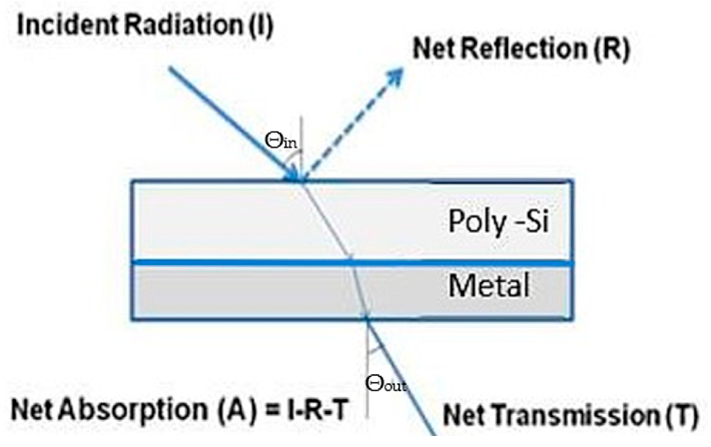
Figure 1. Schematic of the absorber, positioned for the incidence radiation.
Computation 12 00108 g001
Figure 2. Three-layer structure for the calculation of transmission and reflection. Medium 1 is air, medium 2 is poly-Si, and medium 3 is a thin metal layer.
Computation 12 00108 g002
Figure 3. Layout of the three media with the incident, reflected and transmitted electromagnetic waves for normal incidence. Medium 1 is air, medium 2 is dielectric and medium 3 is metal.
Computation 12 00108 g003
Figure 4. Absorption as a function of frequency for the double-layered absorber.
Computation 12 00108 g004
Figure 5. Linear relationship between the wavelength of interest and the corresponding poly-Si thickness optimizing absorption, for the terahertz spectrum [2.5–10 THz or 30–120 μm] on the left and the IR spectrum (3–14 μm) on the right.
Computation 12 00108 g005
Figure 6. Absorptance plots of the double-layered absorber, optimized for the MWIR spectral region on the right and the LWIR spectral region on the left.
Computation 12 00108 g006
Figure 7. Optimal thickness values calculated through the generalized Equation (9) (blue line) and the wide-spectrum linear Equation (10) (red line) versus wavelength.
Computation 12 00108 g007
Table 1. Numerical values of the appropriate poly-Si thickness for the optimization of the double-layered absorber at the wavelength of interest (THz spectrum).
Fixed ValuesWavelength of Interest [μm]Required Poly-Si
Thickness [μm]
  • Poly-Si Refractive index = 5.2
  • Metal’s Sheet resistance = 15 Ω/square
  • Normal incidence
120 (2.5 THz)5.743
60 (5 THz)2.863
40 (7.5 THz)1.903
30 (10 THz)1.423
Table 2. Numerical values of the appropriate poly-Si thickness for the optimization of the double-layered absorber at the wavelength of interest (IR spectrum).
Fixed ValuesWavelength of Interest [μm]Required Poly-Si
Thickness [μm]
  • Poly-Si Refractive index = 5.2
  • Metal’s Sheet resistance = 15 Ω/square
  • Normal incidence
140.655
80.367
50.223
30.127
Disclaimer/Publisher’s Note: The statements, opinions and data contained in all publications are solely those of the individual author(s) and contributor(s) and not of MDPI and/or the editor(s). MDPI and/or the editor(s) disclaim responsibility for any injury to people or property resulting from any ideas, methods, instructions or products referred to in the content.