Article

Charging Effect by Fluorine-Treatment and Recess Gate for Enhancement-Mode on AlGaN/GaN High Electron Mobility Transistors

1
DMC Convergence Research Department, Electronics and Telecommunications Research Institute (ETRI), Daejeon 34129, Korea
2
Center for Emerging Electronic Devices and Systems (CEEDS), Gwangju Institute of Science and Technology (GIST), Gwangju 61005, Korea
*
Author to whom correspondence should be addressed.
Nanomaterials 2020, 10(11), 2116; https://doi.org/10.3390/nano10112116
Submission received: 7 October 2020 / Revised: 20 October 2020 / Accepted: 22 October 2020 / Published: 24 October 2020
(This article belongs to the Section Nanoelectronics, Nanosensors and Devices)

Abstract

:
An enhancement-mode AlGaN/GaN metal-insulator-semiconductor high-electron- mobility-transistor was fabricated using a recess gate and CF4 plasma treatment to investigate its reliable applicability to high-power devices and circuits. The fluorinated-gate device showed hysteresis during the DC current-voltage measurement, and the polarity and magnitude of hysteresis depend on the drain voltage. The hysteresis phenomenon is due to the electron trapping at the Al2O3/AlGaN interface and charging times longer than milliseconds were obtained by pulse I-V measurement. In addition, the subthreshold slope of the fluorinated-gate device was increased after the positive gate bias stress because of the two-dimensional electron gas reduction by ionized fluorine. Our systematic observation revealed that the effect of fluorine ions should be considered for the design of AlGaN/GaN power circuits.

1. Introduction

AlGaN/GaN high electron mobility transistors (HEMTs) have recently demonstrated to be excellent devices for high-frequency and high-power electronics, thanks to the high breakdown voltage [1] and the low on-state resistance [2] and gate leakage [3]. The AlGaN/GaN HEMTs show normally on operation, since the two-dimensional electron gas (2DEG) channel is generated by the spontaneous and piezoelectric polarization at the AlGaN/GaN hetero-interface [4]. Various methods for enhancement mode (E-mode) device manufacturing through modulating the threshold voltage (VT) have been studied for the reduction in power consumption and circuit producing, such as an inverter using a depletion mode (D-mode) and an E-mode device [5,6,7,8,9]. The AlGaN barrier recess and fluorine ion implantation methods had been widely studied to shift the VT in the positive direction.
Although these methods modulate the VT, the gate modifications introduce side effects resulting from the surface damage during the device fabrication process [10,11,12], and the electrical and frequency characteristics are degraded due to the poor interface conditions [13]. Various methods have been studied to improve the recessed interface condition [14,15]. However, hysteresis and VT instability remain critical issues so far. In this perspective, it is necessary to better understand the degradation mechanisms and the trends of changing electrical properties related to charge trapping for reliable application.
In this study, the VT was modulated by the gate recess and fluorine treatment employing CF4 plasma. The fluorinated-gate device (7-nm thick gate recess + fluorine plasma treatment) exhibited more positive-shifted VT compared to the recess only gate device (7-nm thick gate recess). However, hysteresis of the fluorinated-gate device occurred during the DC current-voltage (I-V) measurement and the hysteresis depended on drain voltage (VD). We demonstrated that the cause of hysteresis was the charge trapping/detrapping effect introduced at the dielectric (Al2O3) and fluorinated AlGaN interface and gate leakage characteristics corresponding to VD. The increase in the subthreshold slope (SS) of the fluorinated-gate device after positive gate bias stress indicated the degradation in the AlGaN/GaN interface and the decrease in 2DEG density. As a result, we have revealed the effect of fluorine treatment on the dielectric/AlGaN and AlGaN/GaN interfaces through experimental evidence.

2. Device Fabrication and Electrical Characterization

The AlGaN/GaN heterostructure was grown by metal-organic chemical vapor deposition (MOCVD) on a sapphire substrate, which consists of a 21-nm AlGaN (26% Al) barrier with a 2-nm GaN cap layer. The Ti/Al/Ni/Au ohmic contact was formed by an E-beam evaporator and annealed at 900 °C for 150 s. After device isolation via phosphorus implantation, a 50-nm SiN passivation layer was deposited by plasma-enhanced chemical vapor deposition (PECVD).
Subsequently, the gate recess area was defined by electron-beam (E-beam) lithography and then the SiN was removed via an inductively-coupled plasma (ICP) etch. In order to obtain the etch rate of the gate region using a digital etch process, O2 plasma ashing (3 min) and 1:10 hydrochloric acid (HCl) dipping (1 min) were repeated 15 times in the test sample. An etch rate of 6.6 Å/cycle was obtained (in Figure 1a). The digital etches of 10 and 21 cycles were conducted with the same etch condition and each device had an etch depth of about 7 and 14 nm. For the fabrication of fluorinated-gate devices, CF4 plasma using reactive ion etching (RIE) was carried out for 30 s on the 7-nm recessed device. After that, Al2O3 with the thickness of 10 nm was deposited at 300 °C by atomic layer deposition (ALD). A T-shaped Ni/Au gate electrode was deposited by an E-beam evaporator. D-mode metal-insulator-semiconductor HEMTs (MIS-HEMTs) without gate recess and fluorine treatment were also prepared as a reference device. Figure 1b illustrates the cross-sectional view of the fabricated E-mode Al2O3/AlGaN/GaN MIS-HEMTs with a recessed gate. The fabricated device geometries are LG = 0.25 μm, WG = 50 μm, LGD = 3.5 μm and LGS = 1 μm. The DC I–V, pulse I–V measurement and stress application (for repetition of stress and measurement) were performed using a Keithley 4200-SCS parameter analyzer. The delay between the stress and measurement was less than tens of milliseconds. Capacitance of the device was measured using an Agilent 4294A impedance analyzer. The voltage was applied to the gate while the source and drain were grounded.

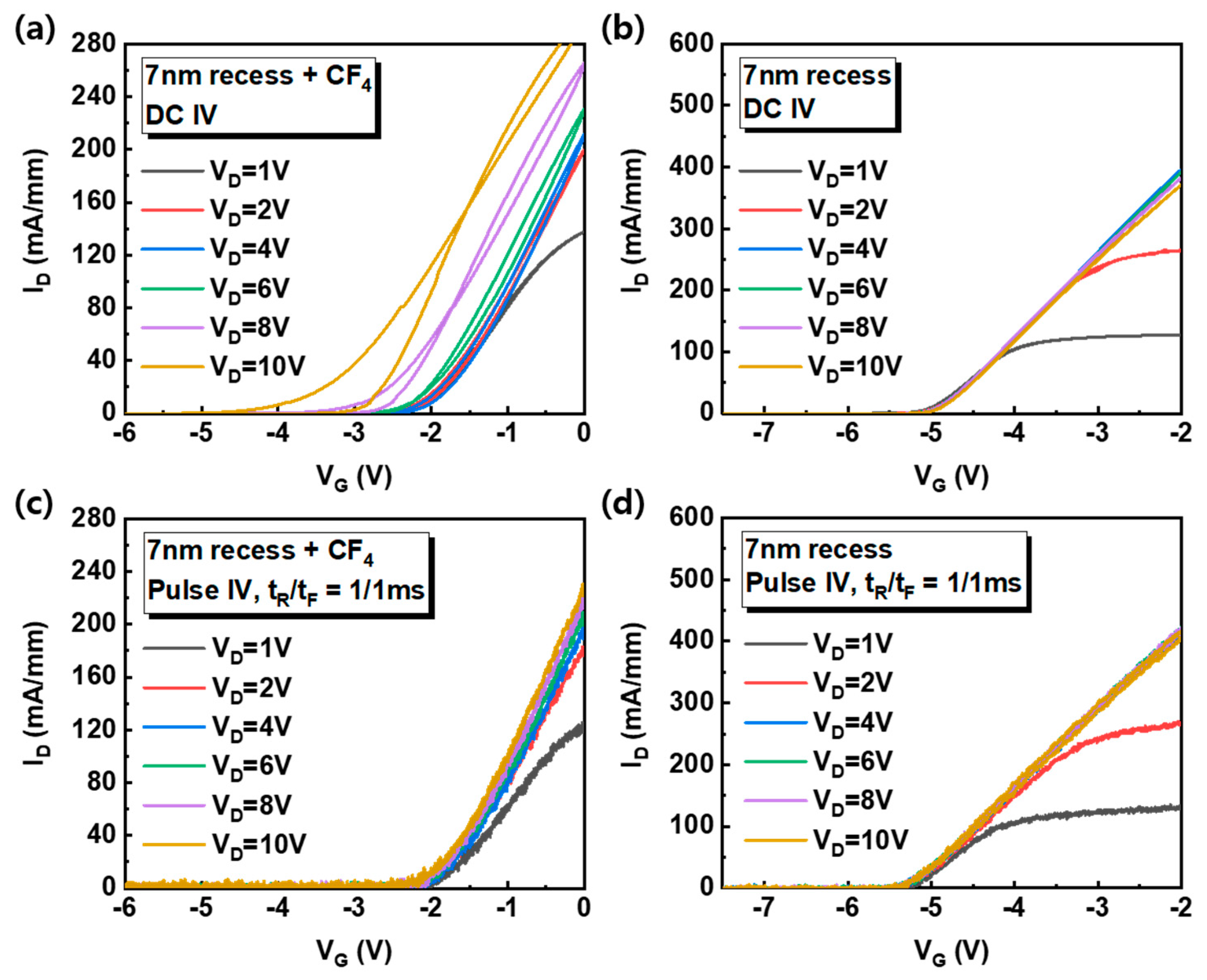
3. Results and Discussion

Figure 2 shows the I-V transfer curves and transconductance (gm) of AlGaN/GaN MIS-HEMTs with various gate condition. The VT moves in the positive direction from the VT of D-MIS-HEMT after the 7-nm gate recess and fluorine treatment, and the VT further shifted after the 14-nm gate recess. The VT depends on the barrier thickness, since the 2DEG concentration and electron mobility reduce with the decrease in AlGaN barrier thickness [16]. The fluorine treatment modulates the VT by incorporating negatively charged fluorine ions into the AlGaN barrier. As a result, the VT of D-MIS-HEMT, 7-nm recess, 7-nm recess + CF4 and 14-nm recess were −6.5, −5.2, −2.5 and +0.5 V, respectively. The VT can be expressed as an Equation (1) [17]. The tb denotes the barrier thickness, φb is the barrier height, q is the electron charge, σp is the 2DEG sheet charge density, NF is the density of ionized fluorine atoms, XF is the triangular fluorine ion distribution peaked at the surface and extending to a given depth and ε and ΔEc are the dielectric constant and conduction band offset, respectively.
V T =   φ b     [ q ( σ p t b N F X F 2 6 ) ε ]     Δ E c
However, the gm of the 7-nm recess + CF4 device decreased sharply after maximum value in comparison with other devices. It is attributed to the electron trap in the AlGaN barrier under the gate region by the fluorine treatment [18]. The 7-nm recess + CF4 device shows hysteresis and it depends on the VD, as shown in Figure 3a. The characteristics of recessed gate (7-nm recess) and fluorinated-gate devices (7 nm-recess + CF4) were discussed to compare the fluorine treatment effect. For the hysteresis and VD effect observation, the VG increased in the forward direction (from the off-state to the on-state) and then decreased again in the reverse direction (from the on-state to the off-state) during the DC I-V measurement for various VD. When the VD is increased from 1 V to 10 V and returned to 1 V, the hysteresis magnitudes (VHysteresis) are almost symmetric. The VHysteresis is the VG difference at a specific ID (= 1 × 10⁻⁷ A/mm). It shows that the DC I-V measurement does not cause permanent charging. However, when the VD is higher than 5 V, the direction of hysteresis becomes negative and the VHysteresis enlarges with increasing VD, as shown in Figure 3c. On the contrary, when the VD is lower than 5 V, the direction of hysteresis is positive and the VHysteresis is relatively small. The negligible hysteresis of recessed gate device without fluorine treatment was achieved (Figure 3b,d).
The VD dependence of hysteresis in the fluorinated-gate device was investigated in more detail by comparing the gate leakage current (IG) as a function of VD in Figure 4a, and the band diagram and IG flow direction are represented in Figure 4b. The IG also depends on the VD, and when the VD is larger than 6 V, the polarity of the IG is negative. This means that the electrons are trapped in the Al2O3/fluorinated-AlGaN barrier as they move from the gate metal to the channel along the IG, and the VT is negatively shifted. However, when the VD is in between −2 V and 6 V, the polarity of IG is positive, showing that some of electrons are detrapped from the Al2O3/fluorinated-AlGaN barrier to the gate metal and the VT is slightly shifted to the positive direction.
The charging time in the Al2O3/fluorinated-AlGaN barrier was studied through a triangular pulse I-V measurement with rising (tR) and falling time (tF) of 1 millisecond (ms). As shown in Figure 5a, the hysteresis and the VD dependence of VT were obtained only in the fluorinated-gate device, whereas insignificant hysteresis was achieved for pulse I-V measurements, and the VT is hardly changed with VD (Figure 5c). However, the transfer curve of recessed gate devices is almost identical regardless of the pulse I-V measurement (Figure 5b,d). Therefore, it implies that the electron trapping/detrapping in the Al2O3/fluorinated-AlGaN barrier is a very slow charging mechanism and the trapping/detrapping time is longer than ms.
To investigate the effect of fluorine in AlGaN under the gate bias stress, negative (−2 V) and positive (+2 V) gate bias stresses were applied to devices. Although the VT of devices is different, the same stress voltage was introduced to compare the effect of the stress polarity (Figure 6). The VD of 5 V was used as a condition to monitor the electrical characteristics of the devices and to minimize the charging effects that occurred during DC I-V measurements. The direction of VT shift under the negative gate bias stress is negative; by contrast, the positive direction of VT shift under the positive gate bias stress is positive, and this phenomenon is the same for both devices. It indicates the trapping (or detrapping) of electrons under the negative (or positive) gate bias stress at the AlGaN/GaN barrier. The different directions of VT shift under negative and positive gate bias stress have been analyzed with the same mechanism in many other studies [19,20,21]. However, in the fluorinated-gate device, the VT moved more, even under other stress conditions (Vstress = VT + 1.0 V and Vstress = +0.5, +1.0 V), as shown in Figure 7a,b, due to the plasma-induced surface damage of the AlGaN barrier during fluorine treatment. In addition, the SS of the fluorinated-gate device is higher than that of the recessed gate device before stress. This indicates a higher interface state and is further evidence of the AlGaN surface damage caused by the CF4 plasma process. Furthermore, the SS of the fluorinated-gate device increased with stress time under the positive gate bias stress, whereas the SS of the recessed gate device without fluorine hardly changed with stress time, even under negative and positive gate bias stress. To observe in more detail, the change in SS is represented in Figure 7c,d. There are two possible origins of the SS increase after gate bias stress. One is the 2DEG reduction. The accelerated electrons from the channel under the positive gate bias stress induce the ionization of fluorine in the AlGaN barrier [22], and the ionized fluorine atoms are capable of forming bonds with gallium atoms with dangling bonds at the interface. The formation of Ga–F bonds is able to weaken the 2DEG channel and AlGaN/GaN interface [23]. Another is the degradation of the AlGaN/GaN interfacial layer by accelerated electrons under positive gate bias stress. For metal-oxide-semiconductor field-effect transistors (MOSFETs), the increase in SS primarily reflects the degradation of the interfacial layer [24,25]. However, the recessed gate device without fluorine did not show an SS change, even under the positive gate bias stress. Therefore, the Ga–F bonding mechanism makes more sense than the interface degradation.
The capacitance–voltage (C–V) curve was measured before and after positive gate bias stress at 1 MHz, as shown in Figure 8a, and the C–V curve moved to a positive direction and the slope of the C–V curve lowered. AlGaN/GaN interface degradation and reduction in 2DEG after positive gate bias stress is also shown. We represent the schematic degradation model of fluorinated-gate device in Figure 8b. At the Al2O3/AlGaN interface, the trapped charges in the border trap site and/or interface state induce hysteresis during DC I-V measurement. The fluorine ions ionized by accelerated electrons by positive gate bias, and formation of the Ga–F bonds induces the reduction in 2DEG at the AlGaN/GaN barrier.

4. Conclusions

An E-mode AlGaN/GaN HEMT was fabricated employing a gate recess and CF4 plasma treatment, and the effect of fluorine in the device was investigated using an analysis of electrical characteristics. The fluorinated-gate device showed hysteresis during DC I-V measurement, which depends on the VD. The pulse I-V measurement was used to observe the charge trapping/detrapping effect of fluorine, and the charging time is longer than a few ms. It was also figured out that the SS of the fluorinated-gate device increased due to the 2DEG reduction by fluorine ions and the formation of Ga–F bonds after positive gate bias stress. We highlight that the impact of fluorine ions should be taken into account for circuit design when the E-mode device is employed.

Author Contributions

Conceptualization and formal analysis and writing, S.C.K.; device fabrication, H.-W.J.; validation, writing—review, investigation and editing, H.-W.J., S.-J.C., H.-K.A. and J.-W.L.; characterization support, S.M.K., S.K.L. and B.H.L.; data analysis, S.K.L., H.K., Y.-S.N., S.-H.L. and S.-I.K.; funding acquisition, H.-K.A. and J.-W.L. All authors have read and agreed to the published version of the manuscript.

Funding

This work was supported by the National Research Council of Science and Technology (NST) grant by the Korean government (MSIT) (No. CRC-19-02-ETRI).

Conflicts of Interest

The authors declare no conflict of interest.

References

  1. Dora, Y.; Chakraborty, A.; Mccarthy, L.; Keller, S.; Denbaars, S.P.; Mishra, U.K. High Breakdown Voltage Achieved on AlGaN/GaN HEMTs With Integrated Slant Field Plates. IEEE Electron Device Lett. 2006, 27, 713–715. [Google Scholar] [CrossRef]
  2. Moens, P.; Banerjee, A.; Uren, M.J.; Meneghini, M.; Karboyan, S.; Chatterjee, I.; Vanmeerbeek, P.; Cäsar, M.; Liu, C.; Salih, A.; et al. Impact of buffer leakage on intrinsic reliability of 650V AlGaN/GaN HEMTs. In Proceedings of the 2015 IEEE International Electron Devices Meeting (IEDM), Washington, DC, USA, 7–9 December 2015; pp. 35.2.1–35.2.4. [Google Scholar]
  3. Ando, Y.; Kaneki, S.; Hashizume, T. Improved operation stability of Al2O3/AlGaN/GaN MOS high-electron-mobility transistors grown on GaN substrates. Appl. Phys. Express 2019, 12, 024002. [Google Scholar] [CrossRef]
  4. Sippel, J.C.; Islam, S.S.; Mukheijee, S.S. A physics-based analytical model of a GaN/AlGaN HEMT incorporating spontaneous and piezoelectric polarization. In Proceedings of the Canadian Conference on Electrical and Computer Engineering 2004 (IEEE Cat. No.04CH37513), Niagara Falls, ON, Canada, 2–5 May 2004; Volume 3, pp. 1401–1404. [Google Scholar]
  5. Chiu, H.-C.; Yang, C.-W.; Chen, C.-H.; Fu, J.S.; Chien, F.-T. Characterization of enhancement-mode AlGaN/GaN high electron mobility transistor using N2O plasma oxidation technology. Appl. Phys. Lett. 2011, 99, 153508. [Google Scholar] [CrossRef]
  6. Palacios, T.; Suh, C.-S.; Chakraborty, A.; Keller, S.; DenBaars, S.P.; Mishra, U.K. High-performance E-mode AlGaN/GaN HEMTs. IEEE Electron Device Lett. 2006, 27, 428–430. [Google Scholar] [CrossRef]
  7. Majumdar, S.; Sahu, C.; Biswas, D. Fabrication of E-mode InGaN/AlGaN/GaN HEMT using FIB based lithography. In Proceedings of the 2017 IEEE Electron Devices Technology and Manufacturing Conference (EDTM), Toyama, Japan, 28 February–2 March 2017; pp. 175–177. [Google Scholar]
  8. Lee, F.; Su, L.-Y.; Wang, C.-H.; Wu, Y.-R.; Huang, J. Impact of Gate Metal on the Performance of p-GaN/AlGaN/GaN High Electron Mobility Transistors. IEEE Electron Device Lett. 2015, 36, 232–234. [Google Scholar] [CrossRef]
  9. Dutta Gupta, S.; Soni, A.; Joshi, V.; Kumar, J.; Sengupta, R.; Khand, H.; Shankar, B.; Mohan, N.; Raghavan, S.; Bhat, N.; et al. Positive Threshold Voltage Shift in AlGaN/GaN HEMTs and E-Mode Operation By AlxTi1−xO Based Gate Stack Engineering. IEEE Trans. Electron Devices 2019, 66, 2544–2550. [Google Scholar] [CrossRef]
  10. Wu, T.-L.; Franco, J.; Marcon, D.; De Jaeger, B.; Bakeroot, B.; Stoffels, S.; Van Hove, M.; Groeseneken, G.; Decoutere, S. Toward Understanding Positive Bias Temperature Instability in Fully Recessed-Gate GaN MISFETs. IEEE Trans. Electron Devices 2016, 63, 1853–1860. [Google Scholar] [CrossRef]
  11. Lagger, P.; Ostermaier, C.; Pobegen, G.; Pogany, D. Towards understanding the origin of threshold voltage instability of AlGaN/GaN MIS-HEMTs. In Proceedings of the 2012 International Electron Devices Meeting, San Francisco, CA, USA, 10–13 December 2012; pp. 13.1.1–13.1.4. [Google Scholar]
  12. Kim, K.-W.; Jung, S.-D.; Kim, D.-S.; Kang, H.-S.; Im, K.-S.; Oh, J.-J.; Ha, J.-B.; Shin, J.-K.; Lee, J.-H. Effects of TMAH Treatment on Device Performance of Normally Off Al2O3/GaN MOSFET. IEEE Electron Device Lett. 2011, 32, 1376–1378. [Google Scholar] [CrossRef]
  13. Jung, H.-W.; Chang, S.-J.; Do, J.-W.; Ahn, H.-K.; Cho, K.-J.; Kim, J.-J.; Kim, S.-I.; Min, B.-G.; Kim, H.; Yoon, H.S.; et al. DC and RF Characteristics of Enhancement-Mode Al2O3/AlGaN/GaN MIS-HEMTs Fabricated by Shallow Recess Combined with Fluorine-Treatment and Deep Recess. ECS J. Solid State Sci. Technol. 2018, 7, 197–200. [Google Scholar] [CrossRef]
  14. Wang, Y.; Wang, M.; Xie, B.; Wen, C.P.; Wang, J.; Hao, Y.; Wu, W.; Chen, K.J.; Shen, B. High-Performance Normally-Off Al2O3/GaN MOSFET Using a Wet Etching-Based Gate Recess Technique. IEEE Electron Device Lett. 2013, 34, 1370–1372. [Google Scholar] [CrossRef]
  15. Li, S.; Hu, Q.; Wang, X.; Li, T.; Li, X.; Wu, Y. Improved Interface Properties and Dielectric Breakdown in Recessed AlGaN/GaN MOS-HEMTs Using HfSiOx as Gate Dielectric. IEEE Electron Device Lett. 2019, 40, 295–298. [Google Scholar] [CrossRef]
  16. Zhao, Y.; Wang, C.; Zheng, X.; Ma, X.; He, Y.; Liu, K.; Li, A.; Peng, Y.; Zhang, C.; Hao, Y. Effects of recess depths on performance of AlGaN/GaN power MIS-HEMTs on the Si substrates and threshold voltage model of different recess depths for the using HfO2 gate insulator. Solid State Electron. 2020, 163, 107649. [Google Scholar] [CrossRef]
  17. Klein, B.A.; Douglas, E.A.; Armstrong, A.M.; Allerman, A.A.; Abate, V.M.; Fortune, T.R.; Baca, A.G. Enhancement-mode Al0.85Ga0.15N/Al0.7Ga0.3N high electron mobility transistor with fluorine treatment. Appl. Phys. Lett. 2019, 114, 112104. [Google Scholar] [CrossRef]
  18. Du, J.; Chen, N.; Jiang, Z.; Bai, Z.; Liu, Y.; Liu, Y.; Yu, Q. Study on transconductance non-linearity of AlGaN/GaN HEMTs considering acceptor-like traps in barrier layer under the gate. Solid State Electron. 2016, 115, 60–64. [Google Scholar] [CrossRef]
  19. Meneghini, M.; Rossetto, I.; Bisi, D.; Ruzzarin, M.; Van Hove, M.; Stoffels, S.; Wu, T.-L.; Marcon, D.; Decoutere, S.; Meneghesso, G.; et al. Negative Bias-Induced Threshold Voltage Instability in GaN-on-Si Power HEMTs. IEEE Electron Device Lett. 2016, 37, 474–477. [Google Scholar] [CrossRef]
  20. Guo, A.; del Alamo, J.A. Unified Mechanism for Positive- and Negative-Bias Temperature Instability in GaN MOSFETs. IEEE Trans. Electron Devices 2017, 64, 2142–2147. [Google Scholar] [CrossRef]
  21. Cheng, L.; Xu, W.; Pan, D.; Liang, H.; Wang, R.; Zhu, Y.; Ren, F.; Zhou, D.; Ye, J.; Chen, D.; et al. Gate-first AlGaN/GaN HEMT technology for enhanced threshold voltage stability based on MOCVD-grown in situ SiNx. J. Phys. Appl. Phys. 2020. [Google Scholar] [CrossRef]
  22. Ma, C.; Chen, H.; Zhou, C.; Huang, S.; Yuan, L.; Roberts, J.; Chen, K.J. ON-state critical gate overdrive voltage for fluorine-implanted enhancement-mode AlGaN/GaN high electron mobility transistors. J. Appl. Phys. 2011, 110, 114514. [Google Scholar] [CrossRef]
  23. Huang, S.; Chen, H.; Chen, K.J. Effects of the fluorine plasma treatment on the surface potential and Schottky barrier height of AlxGa1−xN/GaN heterostructures. Appl. Phys. Lett. 2010, 96, 233510. [Google Scholar] [CrossRef]
  24. Kang, S.C.; Kim, S.M.; Jung, U.; Kim, Y.; Park, W.; Lee, B.H. Interface state degradation during AC positive bias temperature instability stress. Solid State Electron 2019, 158, 46–50. [Google Scholar] [CrossRef]
  25. Cho, M.; Roussel, P.; Kaczer, B.; Degraeve, R.; Franco, J.; Aoulaiche, M.; Chiarella, T.; Kauerauf, T.; Horiguchi, N.; Groeseneken, G. Channel Hot Carrier Degradation Mechanism in Long/Short Channel $n$-FinFETs. IEEE Trans. Electron Devices 2013, 60, 4002–4007. [Google Scholar] [CrossRef]
Figure 1. The fabricated AlGaN/GaN MIS-HEMTs on sapphire substrate. Recessed gate was formed under gate region for VT modulation. (a) The TEM image of the recessed gate. The AlGaN layer was etched by the digital etch process in 15 cycles. (b) Schematic cross-section of the processed device. (c) Band diagram of MIS-HEMTs under equilibrium condition. (d) Band diagram of MIS-HEMTs after CF4 treatment under equilibrium condition.
Nanomaterials 10 02116 g001
Figure 2. The I-V transfer curves (solid line) and transconductance (open circle line) of AlGaN/GaN MIS-HEMTs with various gate conditions at VD = 10 V. Black, blue, red and pink colors indicate the D-mode device, 7-nm gate recessed, 7-nm gate recessed and CF4 treatment and 14-nm gate recessed device, respectively.
Nanomaterials 10 02116 g002
Figure 3. (a,b) The I-V hysteresis curves of 7-nm recess + CF4 and 7-nm recess devices measured at VD = 2 V and 8 V, respectively. The solid line and circle line indicate the forward and reverse sweep, respectively. (c,d) The voltage difference of 7-nm recess + CF4 and 7-nm recess devices by hysteresis at various VD. Red and blue regions show the positive and negative direction of hysteresis, respectively.
Nanomaterials 10 02116 g003
Figure 4. (a) The gate leakage current of the 7-nm recess + CF4 device for various VD. The solid lines and open circles reflect the increase in VD and decrease of VD, respectively. (b) The band diagram of the 7-nm recess + CF4 device. The blue and red arrows indicate the flow of gate current. The trapped charges at the dielectric/AlGaN interface reduce by positive gate current (VD < 5 V) and the trapped charges increase by negative gate current (VD > 5 V).
Nanomaterials 10 02116 g004
Figure 5. (a,b) The dual swept DC I-V transfer curve of 7-nm recess + CF4 and 7-nm recess devices measured at various VD. (c,d) Pulsed I-V curve of 7-nm recess + CF4 and 7-nm recess devices measured for various VD. The rising and falling time of 1 ms was used for pulse measurement.
Nanomaterials 10 02116 g005
Figure 6. (a,b) The change in I-V transfer curves of the 7-nm recess + CF4 device under negative and positive gate bias stress conditions according to stress time, respectively. (c,d) The change in I-V transfer curves of the 7-nm recess device under negative and positive gate bias stress conditions, respectively.
Nanomaterials 10 02116 g006
Figure 7. The VT shift by gate bias stress according to stress time. A (a) negative (VT + 1.0 V) and (b) positive gate bias stress were applied to the devices. The red and black circle line indicate the 7-nm recess + CF4 and 7-nm recess devices, respectively. (c,d) The change in the subthreshold slope for various gate bias stress corresponding to the stress time. The negative biases near the VT and positive bias at 1.0 V and 2.0 V were used to estimate the degradation phenomenon.
Nanomaterials 10 02116 g007
Figure 8. (a) The change in capacitance of the 7-nm recess + CF4 device before and after positive gate bias stress for 1000 s. The closed circle and opened circle indicate the capacitance before and after stress, respectively. (b) Schematic representation of the model used to explain the VT shift of the 7-nm recess + CF4 device. The black circle and red X represent the border traps and interface states, respectively.
Nanomaterials 10 02116 g008
Publisher’s Note: MDPI stays neutral with regard to jurisdictional claims in published maps and institutional affiliations.

