Review

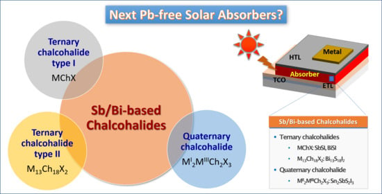
Recent Progress in Fabrication of Antimony/Bismuth Chalcohalides for Lead-Free Solar Cell Applications

Division of Energy Technology, Daegu Gyeongbuk Institute of Science & Technology (DGIST), Daegu 42988, Korea
*
Author to whom correspondence should be addressed.
Nanomaterials 2020, 10(11), 2284; https://doi.org/10.3390/nano10112284
Submission received: 21 October 2020 / Revised: 7 November 2020 / Accepted: 12 November 2020 / Published: 18 November 2020
(This article belongs to the Special Issue Nanostructures for Solar Cells and Photovoltaics)

Abstract

:
Despite their comparable performance to commercial solar systems, lead-based perovskite (Pb-perovskite) solar cells exhibit limitations including Pb toxicity and instability for industrial applications. To address these issues, two types of Pb-free materials have been proposed as alternatives to Pb-perovskite: perovskite-based and non-perovskite-based materials. In this review, we summarize the recent progress on solar cells based on antimony/bismuth (Sb/Bi) chalcohalides, representing Sb/Bi non-perovskite semiconductors containing chalcogenides and halides. Two types of ternary and quaternary chalcohalides are described, with their classification predicated on the fabrication method. We also highlight their utility as interfacial layers for improving other solar cells. This review provides clues for improving the performances of devices and design of multifunctional solar systems.

Graphical Abstract

1. Introduction

Since the Snaith group reported the 10.9% milestone power conversion efficiency (PCE) required for industrial applications for lead-based perovskite (Pb-perovskite) solar cells in 2012 [1], many types of Pb-perovskite solar cells have been fabricated, with performance significantly improving over the past few years [2,3,4,5,6,7]. At present, the certified PCE exceeds 25% [8], approaching the theoretical maximum efficiency for multi-junction Pb-perovskite solar cells [9]. This efficiency is also comparable to those of commercial solar systems based on Si, CdTe, and Cu(In,Ga)Se2. Moreover, high-performance Pb-perovskite solar cells can be manufactured through solution processing at a low temperature of <150 °C, which can reduce costs. Therefore, these characteristics make them the most promising alternative to current photovoltaic systems. However, Pb-perovskite solar cells exhibit limitations for commercialization, with potential health problems and stability being the two main barriers [6,7,10,11,12,13,14,15]. In particular, Pb can be easily released from the Pb-perovskite because of its instability, which can cause major health problems [10,11,12,13,14,15]. Although techniques of material and interface engineering, surface passivation, and encapsulation can significantly improve the stability of Pb-perovskite [7,15,16,17], thereby minimizing the Pb loss, the persistent toxicity problem requires attention to enhance commercialization.
To address these issues, many researchers have focused on finding Pb-free and stable materials with comparable optoelectronic properties. The Pb-free photovoltaic materials proposed as alternatives to date are presented in Table 1. Replacing Pb by tin (Sn) or germanium (Ge), with similar ionic radius and belonging to the same group of the periodic table, in Pb-perovskites is a simple method for fabricating Pb-free materials while maintaining the perovskite structure. These materials are known as Pb-free perovskites. In particular, Sn-based perovskites ASnX3 (A = Cs+, organic cations; X = Cl, I, and Br) exhibit properties comparable to those of Pb-perovskites such as optimal band gaps (Egs) of 1.1–1.4 eV, high carrier mobilities, long carrier lifetimes, and long diffusion lengths [10,11]. Thus, many researchers have devoted attention to developing Sn-based perovskite solar cells [10,11]. Consequently, a record PCE of 11.4% was achieved through the FASnI3 (FA = CH5N2+) solar cell by introducing a phenylhydrazine hydrochloride [18]. However, Sn-perovskites still involve the serious disadvantage of rapid decomposition because Sn is readily oxidized from the +2 to +4 state on exposure to air [10,11]. Another approach for fabricating Pb-free perovskites involves replacing two Pb2+ ions with ions of two metals with oxidation states of +1 and +3 to form double perovskites represented as A2MIMIIIX6 [12,19], with the Cs2AgBiBr6 as a typical example. Alternatively, the two Pb2+ ions are replaced by a tetravalent metal ion, such as Sn4+ or Ti4+, forming compounds with the general formula A2MIVX6 [12,20]. Such compounds are termed vacancy-ordered double perovskites, with the Cs2SnI6 as a prime example. In addition, two-dimensional (2D) perovskites A 3 M 2 III X 9 are produced by replacing the Pb2+ ions with trivalent metal ions such as Sb3+ or Bi3+ [15,21]. Although these Pb-free double and 2D perovskites display significant stability improvement over Pb- and Sn-perovskites, efficiency remains a limitation.
Apart from these Pb-free perovskites, antimony/bismuth (Sb/Bi)-based non-perovskites are another alternative to Pb-perovskites. Unlike perovskites, most of these non-perovskites crystallize in a layered structure, with the layers linked by weak van der Waals forces. This anisotropic crystal structure provides unique and interesting properties that can significantly affect photovoltaic performance [25,26,27]. To date, many Sb/Bi non-perovskites for solar cells have been reported, and these comprise two types, according to elemental composition. The first type is the Sb chalcogenides involving an orthorhombic structure, such as the Sb2Ch3 and CuSbCh2 (Ch = S, Se). In fact, studies on these as photovoltaic materials predates those of Pb-perovskites because of their promising properties, such as the tunable Eg values of 1.0–1.8 eV, high visible light absorption coefficient, stability, low toxicity, and earth-abundant constituents [25,26]. Although varied engineering methods and device architectures have been employed to achieve high-efficiency for Sb chalcogenide solar cells, the performances of these cells remained below the 10% milestone until 2018 [26,27,28,29,30,31,32,33,34,35]. However, recently, a PCE of 9.2% was obtained from the [001]-oriented Sb2Se3 nanorod solar cells [36], and finally, a PCE of 10.5% was reported by Chen’s group from the hydrothermally deposited Sb2(S,Se)3 thin film solar cells [22,37].
Sb/Bi chalcohalides represent the other type of Sb/Bi non-perovskites, comprising Sb/Bi-based semiconductors containing halides and chalcogenides. Following the initial application of Sb sulfoiodide (SbSI) in solar cells by the Seok group in 2018 [38], multiple Sb/Bi chalcohalide solar cells have been proposed. Thus far, the materials investigated for use in solar cells include ternary (MChX and M13Ch18X2, where M = Sb, Bi) [23,38,39,40,41,42,43,44,45,46,47,48,49,50,51,52,53] and quaternary chalcohalides ( M 2 II M III Ch 2 X 3 , where MII = Sn, Pb; MIII = Sb, Bi) [24,54]. These chalcohalides commonly exhibit advantageous properties that can be adjusted for use in solar cells. In particular, the electronic structure of the most studied MChX family is similar to that of Pb-perovskites, with beneficial properties for solar cells such as high dielectric constant, low effective mass, and tunable Eg [39,42,43,44,55]. Therefore, high-performance MChX solar cells comparable to Pb-perovskite cells are expected due to these properties. Recently, the Seok group reported a PCE of 4.07% for Sb0.67Bi0.33SI solar cells, highlighting the high-efficiency potential for the MChX family [23]. In addition, the MChX family is suitable for other applications including the fabrication of room-temperature radiation detectors and p-type transparent conductors [39]. This wide-ranging applicability facilitates designing multifunctional devices. In addition to the MChX family, PCEs of 0.85% and 4.04% have been reported for solar cells based on M13Ch18X2 and M 2 II M III Ch 2 X 3 , respectively. However, the highest PCE achieved for Sb/Bi chalcohalide solar cells remains at around 4%, although the performance has significantly improved over the past few years.
Here, we focus on Sb/Bi-based chalcohalides, including emerging solar material such as MChX compounds, since this type of non-perovskites lack a comprehensive review. Therefore, an up-to-date review summarizing the rapid development of Sb/Bi chalcohalide solar cells and highlighting future research directions is necessary. In this review, we aim to summarize the advances in Sb/Bi chalcohalide solar cells research. To this end, we briefly introduce the crystal and energy band structures of Sb/Bi chalcohalides. Then, we classify these materials based on the fabrication method and discuss their photovoltaic performances. Furthermore, we highlight their usage as interfacial layers for enhancing solar cells. This review presents a step toward the production of high-performance Pb-free non-perovskite chalcohalide solar cells. Note that we have excluded perovskite-based chalcohalide such as (CH3NH3)SbSI2 [56] from this review.

2. Crystal and Energy Band Structures of Sb/Bi Chalcohalides

In this section, the crystal and energy band structures of Sb/Bi chalcohalides used to date for solar cells are briefly presented. Depending on the number of elements and composition, Sb/Bi chalcohalides with different structures can be created, as shown in Table 2. The ternary chalcohalides employed for solar cells are the MChX and M13Ch18X2 types. The MChX type, such as SbSI and BiSI, involves the orthorhombic structure with the Pnma space group, crystallizing into an [(MChX)2]n double-chained structure, with the adjacent chains joined by van der Waals forces [57,58]. Conversely, the M13Ch18X2 type such as the Bi3S18I2 possesses a hexagonal structure with a ribbon-shaped (M4Ch6) subunit. The M4Ch6 subunits form six spokes around the central hexagonal channel at the corners of the unit cell, with iodine in between [53,58]. For the quaternary chalcohalides ( M 2 II M III Ch 2 X 3 ), such as Pb2SbS2I3 and Sn2SbS2I3, crystallization produces the orthorhombic structure with the Cmcm space group [24,54,59].
To employ Sb/Bi chalcohalides in solar cells, the energy band structure deserves priority because of its importance in light harvesting and conversion. Specifically, the Eg should be checked because it determines the maximum PCE achievable for each material according to the Shockley–Queisser limit [60,61]. Thus, materials with an Eg value between 1.10 and 1.55 eV are preferred for solar cells. Figure 1 displays the energy band diagram of typical Sb/Bi chalcohalides reported to date. The positions of the conduction band minimum and valence band maximum as well as the Eg value vary depending on the elemental composition and number of elements. Along with the chalcohalides shown in Figure 1, Sb/Bi chalcohalides exhibit Eg values varying from 0.75 eV for Bi13S18I2 [53] to 2.31 eV for SbSBr [42]. These results indicate that their band structures can be tuned via chemical substitution, and that the electron transporting layer (ETL) and hole transporting layer (HTL) applications necessitate selectivity for each solar cell depending on the chalcohalide used. In addition to the band structures, other factors such as the optical absorption strength, charge effective mass, dielectric constant, and defects require consideration [44,61]. However, research on these remains insufficient, and this highlights the need for further studies.

3. Theoretical Insights on Sb/Bi Chalcohalides as Solar Absorbers

Theoretical calculations, such as first-principle methods, provide further insight into the potential of specific materials (e.g., as solar absorbers) and clues for designing device structures. However, the research on such theoretical investigations is very limited because Sb/Bi chalcohalide solar cells are still in their early stages of development compared to the Pb-perovskite cells. Thus, in this section, theoretical insights into only the most studied MChX family are briefly introduced.
Based on the first-principle calculations, Brandt et al. identified the MChX family as promising solar absorbers due to its low effective masses, large dielectric constants, and strong absorption, as shown in Table 3 [62]. They further found that BiSI and BiSeI are most suitable for achieving high-performance solar cells because of their much stronger spin-orbit coupling. The suitability of these Bi compounds for solar cells was also confirmed by other groups [39,43,44,63]. Ganose et al. suggested that the conducting oxide and HTL should be selected for efficient charge transfers by considering the electron affinity (EA = 4.9–5.0 eV) and ionized potential (IP = 6.2–6.4 eV) of these Bi chalcohalides, respectively [43]. They also concluded from the defect analysis that these Bi compounds represent intrinsic semiconductors regardless of fabrication conditions, making them best suited for application in p-i-n device architecture [44].
Butler et al. analyzed the band structures of SbChX (SbSI, SbSeI, and SbSBr) by different calculation methods [42,55]. The effective masses were calculated to be below 0.65, indicating that SbChX have high charge carrier mobilities suitable for solar cells. They also found that the SbSBr have deeper IP energy (5.8 eV) than that of I-containing SbChX (5.3 eV for SbSeI and 5.4 eV for SbSI). This different IP energy suggests that contacting layers such as ETL and HTL should be selected depending on the halide ion of SbChX for optimal device performance [42]. For example, the contacting layers used in Cu2ZnSnS4 (CZTS) can be applied to SbSBr solar cells due to their similar IP value with that of CZTS. In addition, a heterojunction structure composed of SbSI/SbSBr with SbSBr epitaxially grown on SbSI was proposed for efficient charge separation based on their closely matched lattice parameters and band offsets [55].

4. Sb/Bi Chalcohalide Solar Cells Fabrication

The fabrication of high-quality materials with adequate morphologies and properties is essential for manufacturing high-performance solar cells. However, methods for producing Sb/Bi chalcohalide solar cells are scant, with those existing lacking the optimization necessary to provide high-efficiency solar cells. Therefore, developing methods to control and optimize the properties of chalcohalides suitable for solar cells is imperative. Sb/Bi chalcohalides used for solar cells are prepared by many techniques including spray pyrolysis [40], spin coating [24,45,46,47,51], solvothermal synthesis [49,53], and mixed techniques [23,38,48,65]. In this section, the fabrication methods reported to date are categorized and described, with the solar cells fabricated presented by the method in Table 4.

4.1. One-Step Deposition

In the one-step method, Sb/Bi chalcohalides are directly deposited using a precursor solution by the spray or spin-coating techniques. Hahn et al. deposited Se-doped BiSI films by spraying a precursor solution on a pre-heated F-doped SnO2 (FTO) substrate at 275 °C [40]. The Se doping levels were controlled by adjusting the concentration of thiourea (TU) and SeO2 in the precursor solution. They found that the morphology changed from microscale rods to cube-like structures as the Se amount increased (Figure 2a). The optical Eg decreased linearly with increasing Se content, as shown in Figure 2b. Then, the researchers applied these Bi(S,Se)I films for solar cell fabrication, obtaining a PCE of 0.012% for an FTO/Pt/CuSCN/BiSI/FTO device.
Recently, Tiwari et al. applied the spin coating technique to the one-step method in fabricating BiSI films [46]. They used a molecular solution synthesized by dissolving Bi(NO3)2·5H2O, TU, and NH4I in a 2-methoxyethanol and acetylacetone mixture for the spin coating. Using this method, flake-shaped BiSI films were produced (Figure 3). To apply these films to solar cells, they used SnO2 and F8 as the ETL and HTL, respectively, obtaining a PCE of 1.32% for an Au/F8/BiSI/SnO2/FTO device (Figure 3b). Similarly, Nishikudo et al. used an Sb(EtX)3 single crystal for a spin coating based on the one-step method [51]. To fabricate SbSI solar cells, the solution, synthesized by dissolving the Sb(EtI)3 single crystal and SbI3 in dimethyl sulfoxide, was spin-coated onto a mesoporous TiO2 (mp-TiO2)/TiO2 blocking layer (TiO2-BL)/FTO substrate and annealed at 200–240 °C. Then, the HTL and Au were sequentially deposited. The Sb2S3-containing SbSI structure obtained at 240 °C exhibited better device performance than that with the SbSI. Furthermore, thiophene-containing HTL such as the poly[2,6-(4,4-bis(2-ethylhexyl)-4H-cyclopenta[2,1-b;3,4-b’]dithiophene)-alt-4,7-(2,1,3-benzothiadiazole) (PCPDTBT) and poly(3-hexylthiophene) (P3HT) was reported to significantly contribute to improving device performance. As a result, they obtained an impressive PCE of 2.91% from the Sb2S3-containing SbSI device involving the PCPDTBT HTL, and the device showed good stability under high humidity (Figure 3c–f). In addition to ternary MChX, the one-step spin-coating method is usable in fabricating quaternary chalcohalides ( M 2 II M III Ch 2 X 3 ). Recently, Nie et al. synthesized a precursor solution by dissolving SbCl3, TU, and SnI2 in N,N-dimethylformamide [24]. Then, the solution was spin-coated on mp-TiO2/TiO2-BL/FTO and annealed to fabricate quaternary Sn2SbS2I3 nanostructures. The as-prepared Sn2SbS2I3 displayed a suitable Eg of 1.41 eV, while the Sn2SbS2I3 device showed a PCE of 4.04% and good stability against humidity.

4.2. Two-Step Deposition Method

In the two-step deposition method, chalcogenides (M2Ch3) are fabricated (step 1) and then converted into chalcohalides (MChX) through the reaction of M2Ch3 and MX3 (step 2). This reaction is expressed in Equation (1).
M2Ch3 + MX3 → 3MChX,
This deposition method was first applied by the Seok group for fabricating SbSI solar cells (Figure 4a) [38]. In step 1, amorphous Sb2S3 was deposited on an mp-TiO2/TiO2-BL/FTO substrate by chemical bath deposition (CBD), accompanied by crystallization at 300 °C. Then, the crystalline Sb2S3 was converted to SbSI by multiple cycles of spin coating with an SbI3 solution, followed by annealing (step 2). A PCE of 3.05% was obtained from an Au/PCPDTBT/SbSI/mp-TiO2/TiO2-BL/FTO solar cell. Furthermore, they fabricated Bi-alloyed SbSI, i.e., Sb0.67Bi0.33SI, using a BiI3 solution instead of SbI3 in step 2 (Figure 4b) [23]. This material absorbs more light, producing a higher short-circuit current density because of its narrower Eg (1.67 eV) than SbSI. Thus, a better PCE (4.07%) was obtained for the Sb0.67Bi0.33SI solar cell compared to the SbSI-based cell. However, this method is time-consuming because it requires multiple cycles in step 2 to obtain complete sulfoiodides. In addition, the resulting films were not completely homogeneous. To overcome these limitations, they introduced an SbI3 vapor process instead of the SbI3 solution process in step 2 (Figure 4c), enabling the production of SbSI with improved homogeneity without repeating step 2 [65] and yielding a better PCE of 3.62% for SbSI solar cells. The study by the Seok group clearly demonstrated a two-step method for fabricating different chalcohalides. However, inherent limitations of the CBD process, such as the formation of impurities and difficulty in controlling the ratio [28,31], may limit the controlled growth of chalcohalides. In addition, factors such as morphology and thickness, which are critical for planar devices, were not considered because the study was optimized for the mesoporous device architecture. Therefore, developing a two-step method allowing the controlled growth of chalcohalides for the planar device architecture remains a challenge.
To apply the two-step method to the planar device architecture, a thin film covering the entire surface is necessary. This is because incomplete surface coverage reduces the ability to absorb light and creates the shunt paths, thereby degrading the device performance [66]. We confirmed the feasibility of forming a compact thin film using a two-step method. We introduced an SbCl3-TU method instead of the CBD method in step 1 [45], enabling control of the Sb/S ratio and minimizing impurity formation [31]. Then, we used a high-concentration solution to lower the need for multiple cycles in step 2, and this modified method is illustrated in Figure 5a. We found that the Sb/S ratio of the solution used in step 1 significantly affected surface coverage (Figure 5b–d). The annealing conditions of step 2 also contributed to controlling the crystallinity. Then, a compact SbSI thin film with high crystallinity was obtained with an Sb/S specific molar ratio of 1:3 at 200 °C, and an impressive PCE of 0.93% was achieved by the SbSI device. This method allowed us to fabricate pure-phase SbSI thin films and to control morphology and structure. Our method can also be applied for fabricating other chalcohalides such as BiSI [47]. To fabricate BiSI films, we introduced a Bi2O3-TU solution based on a thiol–amine solvent and BiI3 solution in steps 1 and 2, respectively (Figure 5e). Using this method, nanorod-based BiSI films with an Eg value of 1.61 eV were obtained (Figure 5f,g). Recently, Xiong et al. also reported the fabrication of BiSI nanorods arrays based on a two-step method [49]. However, their method involved the solvothermal synthesis instead of spin coating in each step, as illustrated in Figure 6a. The BiSI nanorods were fabricated by immersing Bi2S3-deposited tungsten (W) foil in an autoclave containing BiI3 solution and subsequent heating. Compared to the spin coating-based two-step process [47], the as-prepared nanorods exhibited a similar Eg value of 1.57 eV but showed preferential [010] orientation. To fabricate solar cells, a p-type CuSCN and an In-doped SnO2 (ITO) were sequentially deposited on the BiSI surface, yielding a PCE of 0.66% (Figure 6b).
The two-step method is also suitable for fabricating the quaternary Pb2SbS2I3. Nie et al. deposited a nanostructured Pb2SbS2I3 with an Eg of 2.19 eV on an mp-TiO2/TiO2-BL/FTO substrate [54] for solar cells by modifying the two-step method used for SbSI fabrication [38]. In the modified method, step 1 was identical to that in the SbSI fabrication, whereas a PbI2 solution was used in step 2. Through optimization, the best PCE obtained from the Au/PCPDTBT/Pb2Sb2S2I3/mp-TiO2/TiO2-BL/FTO device was 3.2%. These results imply that the two-step method can be simply applied for fabricating Sb/Bi chalcohalides by selecting an appropriate source or reagent in each step.

4.3. Other Methods

In addition to the two methods described above, Sb/Bi chalcohalides are fabricated using other approaches. Kunioku et al. reported a low-temperature method based on Bi oxyhalide (BiOX) particles for fabricating Bi chalcohalides (BiChX) [41]. The BiChX were fabricated by substituting Ch2− for the O2− of BiOX particles under H2(S,Se) gas. Thus, Bi chalcohalides such as BiSI, BiSeI, BiSSeI, and BiSBr1−xIx were obtained by adjusting the starting BiOX and gas type, as shown in Figure 7a. This method enabled BiChX fabrication with controllable Eg at low temperature (<150 °C). BiSI and BiSeI have also been fabricated by a ball milling method [52]. In addition, one-dimensional SbSI nanostructures were independently manufactured using a mixed sonication–heating method [48] and sonochemical synthesis [50]. Recently, Li et al. fabricated a new type of ternary Bi chalcohalide, the tetragonal Bi13S18I2, in addition to BiSI, with both controlled by adjusting the mole ratio of CH4N2S/BiI3/CH3NH3I (CH3NH3I = MAI) in the solution used in the solvothermal process (Figure 7b) [53]. They found that a pure Bi13S18I2 structure can be obtained from the conversion reaction of BiSI over 6 h at a CH4N2S/BiI3/MAI ratio of 4:2:3. The Bi13S18I2 device exhibited a PCE of 0.85% (Figure 7c), demonstrating the potential of Bi13S18I2 as a light absorber for solar cells.

5. Sb/Bi Chalcohalides as Interfacial Layer

In addition to being used as light absorbers in solar cells, Sb/Bi chalcohalides can be also used as interfacial layers. Yoo et al. used BiSI as an interlayer in a BiI3 solar cell at the interface between the ETL and BiI3 light absorber [67]. The BiSI layer was formed in situ on the ETL surface by the reaction of In2S3 and BiI3 at 200 °C during BiI3 deposition. The BiSI interlayer greatly improved the hole transfer from BiI3 to HTL, improving the PCE to 1.21%. Other chalcohalides can also serve as interlayers. According to the Seok group, the SbSI interlayer formed on the Sb2S3 surface provides an energetically favorable driving force for photogenerated carriers [65]. Thus, the SbSI-interlayered Sb2S3 device showed better performance than the Sb2S3 device, with the best PCE of 6.08%.

6. Summary and Outlook

In this review, we summarized the recent progress on the fabrication of Sb/Bi chalcohalide solar cells by focusing on the fabrication methods. Two types of Sb/Bi chalcohalides have been manufactured as Pb-free solar absorbers for solar cells by one-step, two-step, and other methods. The first involves ternary chalcohalides (MChX and M13Ch18X2), while the other comprises quaternary chalcohalides ( M 2 II M III Ch 2 X 3 ). Maximum PCEs of 4.07% and 4.04% were obtained from the ternary Sb0.67Bi0.33SI and quaternary Sn2SbS2I3 solar cells, respectively. In addition, ternary BiSI and SbSI acted as interfacial layers in solar cells, contributing to enhanced charge transfer. Although Sb/Bi chalcohalides with excellent stability have been proposed over the past few years, their PCEs still significantly lag behind those of Pb-perovskites. Therefore, an in-depth comprehensive investigation into the intrinsic and extrinsic factors affecting device performance is required. The impact of material composition, morphology, device architecture, crystal orientation, and interfacial layer, as well as the factors affecting performance degradation and device stability, also require detailed examination to further improve the performance of devices [61,66,68].

Author Contributions

Conceptualization, Y.C.C.; Supervision, Y.C.C.; Project Administration, Y.C.C.; Investigation, Y.C.C. and K.-W.J.; Writing—Original Draft Preparation, Y.C.C.; Writing—Review and Editing, Y.C.C. and K.-W.J. All authors have read and agreed to the published version of the manuscript.

Funding

This work was supported by the National Research Foundation of Korea (NRF) grant funded by the Korea government (MSIT) (No. 2019R1F1A1049014). This work was also supported by the DGIST R&D program of the Ministry of Science and ICT, Republic of Korea (No. 20-ET-08).

Conflicts of Interest

The authors declare no conflict of interest.

References

  1. Lee, M.M.; Teuscher, J.; Miyasaka, T.; Murakami, T.N.; Snaith, H.J. Efficient Hybrid Solar Cells Based on Meso-Superstructured Organometal Halide Perovskites. Science 2012, 338, 643–647. [Google Scholar] [CrossRef] [Green Version]
  2. Choi, Y.C.; Lee, S.W.; Jo, H.J.; Kim, D.-H.; Sung, S.-J. Controlled growth of organic-inorganic hybrid CH3NH3PbI3 perovskite thin films from phase-controlled crystalline powders. RSC Adv. 2016, 6, 104359–104365. [Google Scholar] [CrossRef]
  3. Choi, Y.C.; Lee, S.W.; Kim, D.-H. Antisolvent-assisted powder engineering for controlled growth of hybrid CH3NH3PbI3 perovskite thin films. APL Mater. 2017, 5, 026101. [Google Scholar] [CrossRef] [Green Version]
  4. Jung, E.H.; Jeon, N.J.; Park, E.Y.; Moon, C.S.; Shin, T.J.; Yang, T.-Y.; Noh, J.H.; Seo, J. Efficient, stable and scalable perovskite solar cells using poly (3-hexylthiophene). Nature 2019, 567, 511. [Google Scholar] [CrossRef] [PubMed]
  5. Seok, S.I.; Grätzel, M.; Park, N.G. Methodologies toward Highly Efficient Perovskite Solar Cells. Small 2018, 14, 1704177. [Google Scholar] [CrossRef] [PubMed]
  6. Jena, A.K.; Kulkarni, A.; Miyasaka, T. Halide perovskite photovoltaics: Background, status, and future prospects. Chem. Rev. 2019, 119, 3036–3103. [Google Scholar] [CrossRef] [PubMed]
  7. Kim, B.; Seok, S.I. Molecular aspects of organic cations affecting the humidity stability of perovskites. Energy Environ. Sci. 2020, 13, 805–820. [Google Scholar] [CrossRef]
  8. Green, M.A.; Dunlop, E.D.; Hohl-Ebinger, J.; Yoshita, M.; Kopidakis, N.; Hao, X. Solar cell efficiency tables (version 56). Prog. Photovolt. 2020, 28, 629–638. [Google Scholar] [CrossRef]
  9. Granas, O.; Vinichenko, D.; Kaxiras, E. Establishing the limits of efficiency of perovskite solar cells from first principles modeling. Sci. Rep. 2016, 6, 36108. [Google Scholar] [CrossRef]
  10. Nasti, G.; Abate, A. Tin Halide Perovskite (ASnX3) Solar Cells: A Comprehensive Guide toward the Highest Power Conversion Efficiency. Adv. Energy Mater. 2020, 10, 1902467. [Google Scholar] [CrossRef]
  11. Hasan, S.A.U.; Lee, D.S.; Im, S.H.; Hong, K.-H. Present Status and Research Prospects of Tin-based Perovskite Solar Cells. Solar RRL 2019, 4, 1900310. [Google Scholar] [CrossRef]
  12. Kung, P.-K.; Li, M.-H.; Lin, P.-Y.; Jhang, J.-Y.; Pantaler, M.; Lupascu, D.C.; Grancini, G.; Chen, P. Lead-Free Double Perovskites for Perovskite Solar Cells. Solar RRL 2019, 4, 1900306. [Google Scholar] [CrossRef]
  13. Miyasaka, T.; Kulkarni, A.; Kim, G.M.; Öz, S.; Jena, A.K. Perovskite Solar Cells: Can We Go Organic-Free, Lead-Free, and Dopant-Free? Adv. Energy Mater. 2020, 10, 1902500. [Google Scholar] [CrossRef]
  14. Nie, R.; Sumukam, R.R.; Reddy, S.H.; Banavoth, M.; Seok, S.I. Lead-free perovskite solar cells enabled by hetero-valent substitutes. Energy Environ. Sci. 2020, 13, 2363–2385. [Google Scholar] [CrossRef]
  15. Jin, Z.; Zhang, Z.; Xiu, J.; Song, H.; Gatti, T.; He, Z. A critical review on bismuth and antimony halide based perovskites and their derivatives for photovoltaic applications: Recent advances and challenges. J. Mater. Chem. A 2020, 8, 16166–16188. [Google Scholar] [CrossRef]
  16. Uddin, A.; Upama, M.; Yi, H.; Duan, L. Encapsulation of Organic and Perovskite Solar Cells: A Review. Coatings 2019, 9, 65. [Google Scholar] [CrossRef] [Green Version]
  17. Wang, R.; Mujahid, M.; Duan, Y.; Wang, Z.K.; Xue, J.; Yang, Y. A Review of Perovskites Solar Cell Stability. Adv. Funct. Mater. 2019, 29, 1808843. [Google Scholar] [CrossRef]
  18. Wang, C.; Gu, F.; Zhao, Z.; Rao, H.; Qiu, Y.; Cai, Z.; Zhan, G.; Li, X.; Sun, B.; Yu, X.; et al. Self-Repairing Tin-Based Perovskite Solar Cells with a Breakthrough Efficiency Over 11%. Adv. Mater. 2020, 32, 1907623. [Google Scholar] [CrossRef]
  19. Yang, X.; Chen, Y.; Liu, P.; Xiang, H.; Wang, W.; Ran, R.; Zhou, W.; Shao, Z. Simultaneous Power Conversion Efficiency and Stability Enhancement of Cs2AgBiBr6 Lead-Free Inorganic Perovskite Solar Cell through Adopting a Multifunctional Dye Interlayer. Adv. Funct. Mater. 2020, 30, 2001557. [Google Scholar] [CrossRef]
  20. Chen, M.; Ju, M.-G.; Carl, A.D.; Zong, Y.; Grimm, R.L.; Gu, J.; Zeng, X.C.; Zhou, Y.; Padture, N.P. Cesium Titanium(IV) Bromide Thin Films Based Stable Lead-free Perovskite Solar Cells. Joule 2018, 2, 558–570. [Google Scholar] [CrossRef] [Green Version]
  21. Yang, Y.; Liu, C.; Cai, M.; Liao, Y.; Ding, Y.; Ma, S.; Liu, X.; Guli, M.; Dai, S.; Nazeeruddin, M.K. Dimension-Controlled Growth of Antimony-Based Perovskite-like Halides for Lead-Free and Semitransparent Photovoltaics. ACS Appl. Mater. Interfaces 2020, 12, 17062–17069. [Google Scholar] [CrossRef] [PubMed]
  22. Wang, X.; Tang, R.; Jiang, C.; Lian, W.; Ju, H.; Jiang, G.; Li, Z.; Zhu, C.; Chen, T. Manipulating the Electrical Properties of Sb2(S,Se)3 Film for High-Efficiency Solar Cell. Adv. Energy Mater. 2020, 10, 2002341. [Google Scholar] [CrossRef]
  23. Nie, R.; Im, J.; Seok, S.I. Efficient Solar Cells Employing Light-Harvesting Sb0.67Bi0.33SI. Adv. Mater. 2019, 31, 1808344. [Google Scholar] [CrossRef] [PubMed]
  24. Nie, R.; Lee, K.S.; Hu, M.; Paik, M.J.; Seok, S.I. Heteroleptic Tin-Antimony Sulfoiodide for Stable and Lead-free Solar Cells. Matter 2020, 3, 1701–1713. [Google Scholar] [CrossRef]
  25. Chen, C.; Tang, J. Open-Circuit Voltage Loss of Antimony Chalcogenide Solar Cells: Status, Origin, and Possible Solutions. ACS Energy Lett. 2020, 5, 2294–2304. [Google Scholar] [CrossRef]
  26. Lei, H.; Chen, J.; Tan, Z.; Fang, G. Review of Recent Progress in Antimony Chalcogenide-Based Solar Cells: Materials and Devices. Solar RRL 2019, 3, 1900026. [Google Scholar] [CrossRef]
  27. Zhou, Y.; Wang, L.; Chen, S.; Qin, S.; Liu, X.; Chen, J.; Xue, D.-J.; Luo, M.; Cao, Y.; Cheng, Y.; et al. Thin-film Sb2Se3 photovoltaics with oriented one-dimensional ribbons and benign grain boundaries. Nat. Photonics 2015, 9, 409–415. [Google Scholar] [CrossRef]
  28. Choi, Y.C.; Lee, D.U.; Noh, J.H.; Kim, E.K.; Seok, S.I. Highly Improved Sb2S3 Sensitized-Inorganic-Organic Heterojunction Solar Cells and Quantification of Traps by Deep-Level Transient Spectroscopy. Adv. Funct. Mater. 2014, 24, 3587–3592. [Google Scholar] [CrossRef]
  29. Choi, Y.C.; Mandal, T.N.; Yang, W.S.; Lee, Y.H.; Im, S.H.; Noh, J.H.; Seok, S.I. Sb2Se3-Sensitized Inorganic-Organic Heterojunction Solar Cells Fabricated Using a Single-Source Precursor. Angew. Chem. Int. Ed. 2014, 53, 1329–1333. [Google Scholar] [CrossRef]
  30. Choi, Y.C.; Lee, Y.H.; Im, S.H.; Noh, J.H.; Mandal, T.N.; Yang, W.S.; Seok, S.I. Efficient Inorganic-Organic Heterojunction Solar Cells Employing Sb2(Sx/Se1−x)3 Graded-Composition Sensitizers. Adv. Energy Mater. 2014, 4, 1301680. [Google Scholar] [CrossRef]
  31. Choi, Y.C.; Seok, S.I. Efficient Sb2S3-Sensitized Solar Cells Via Single-Step Deposition of Sb2S3 Using S/Sb-Ratio-Controlled SbCl3-Thiourea Complex Solution. Adv. Funct. Mater. 2015, 25, 2892–2898. [Google Scholar] [CrossRef]
  32. Choi, Y.C.; Yeom, E.J.; Ahn, T.K.; Seok, S.I. CuSbS2-Sensitized Inorganic-Organic Heterojunction Solar Cells Fabricated Using a Metal-Thiourea Complex Solution. Angew. Chem. Int. Ed. 2015, 54, 4005–4009. [Google Scholar] [CrossRef] [PubMed]
  33. Chen, C.; Li, K.; Chen, S.; Wang, L.; Lu, S.; Liu, Y.; Li, D.; Song, H.; Tang, J. Efficiency Improvement of Sb2Se3 Solar Cells via Grain Boundary Inversion. ACS Energy Lett. 2018, 3, 2335–2341. [Google Scholar] [CrossRef]
  34. Wu, C.; Zhang, L.; Ding, H.; Ju, H.; Jin, X.; Wang, X.; Zhu, C.; Chen, T. Direct solution deposition of device quality Sb2S3−xSex films for high efficiency solar cells. Sol. Energy Mater. Sol. Cells 2018, 183, 52–58. [Google Scholar] [CrossRef]
  35. Tang, R.; Wang, X.; Jiang, C.; Li, S.; Jiang, G.; Yang, S.; Zhu, C.; Chen, T. Vacuum assisted solution processing for highly efficient Sb2S3 solar cells. J. Mater. Chem. A 2018, 6, 16322–16327. [Google Scholar] [CrossRef]
  36. Li, Z.; Liang, X.; Li, G.; Liu, H.; Zhang, H.; Guo, J.; Chen, J.; Shen, K.; San, X.; Yu, W.; et al. 9.2%-efficient core-shell structured antimony selenide nanorod array solar cells. Nat. Commun. 2019, 10, 125. [Google Scholar] [CrossRef] [Green Version]
  37. Tang, R.; Wang, X.; Lian, W.; Huang, J.; Wei, Q.; Huang, M.; Yin, Y.; Jiang, C.; Yang, S.; Xing, G.; et al. Hydrothermal deposition of antimony selenosulfide thin films enables solar cells with 10% efficiency. Nat. Energy 2020, 5, 587–595. [Google Scholar] [CrossRef]
  38. Nie, R.; Yun, H.-S.; Paik, M.-J.; Mehta, A.; Park, B.-W.; Choi, Y.C.; Seok, S.I. Efficient Solar Cells Based on Light-Harvesting Antimony Sulfoiodide. Adv. Energy Mater. 2017, 8, 1701901. [Google Scholar] [CrossRef]
  39. Shi, H.; Ming, W.; Du, M.-H. Bismuth chalcohalides and oxyhalides as optoelectronic materials. Phys. Rev. B 2016, 93, 104108. [Google Scholar] [CrossRef] [Green Version]
  40. Hahn, N.T.; Rettie, A.J.E.; Beal, S.K.; Fullon, R.R.; Mullins, C.B. n-BiSI Thin Films: Selenium Doping and Solar Cell Behavior. J. Phys. Chem. C 2012, 116, 24878–24886. [Google Scholar] [CrossRef]
  41. Kunioku, H.; Higashi, M.; Abe, R. Low-Temperature Synthesis of Bismuth Chalcohalides: Candidate Photovoltaic Materials with Easily, Continuously Controllable Band gap. Sci. Rep. 2016, 6, 32664. [Google Scholar] [CrossRef] [PubMed]
  42. Butler, K.T.; McKechnie, S.; Azarhoosh, P.; van Schilfgaarde, M.; Scanlon, D.O.; Walsh, A. Quasi-particle electronic band structure and alignment of the V-VI-VII semiconductors SbSI, SbSBr, and SbSeI for solar cells. Appl. Phys. Lett. 2016, 108, 112103. [Google Scholar] [CrossRef] [Green Version]
  43. Ganose, A.M.; Butler, K.T.; Walsh, A.; Scanlon, D.O. Relativistic electronic structure and band alignment of BiSI and BiSeI: Candidate photovoltaic materials. J. Mater. Chem. A 2016, 4, 2060–2068. [Google Scholar] [CrossRef] [Green Version]
  44. Ganose, A.M.; Matsumoto, S.; Buckeridge, J.; Scanlon, D.O. Defect Engineering of Earth-Abundant Solar Absorbers BiSI and BiSeI. Chem. Mater. 2018, 30, 3827–3835. [Google Scholar] [CrossRef] [PubMed]
  45. Choi, Y.C.; Hwang, E.; Kim, D.-H. Controlled growth of SbSI thin films from amorphous Sb2S3 for low-temperature solution processed chalcohalide solar cells. APL Mater. 2018, 6, 121108. [Google Scholar] [CrossRef] [Green Version]
  46. Tiwari, D.; Cardoso-Delgado, F.; Alibhai, D.; Mombrú, M.; Fermín, D.J. Photovoltaic Performance of Phase-Pure Orthorhombic BiSI Thin-Films. ACS Appl. Energy Mater. 2019, 2, 3878–3885. [Google Scholar] [CrossRef]
  47. Choi, Y.C.; Hwang, E. Controlled Growth of BiSI Nanorod-Based Films Through a Two-Step Solution Process for Solar Cell Applications. Nanomaterials 2019, 9, 1650. [Google Scholar] [CrossRef] [Green Version]
  48. Pathak, A.K.; Prasad, M.D.; Batabyal, S.K. One-dimensional SbSI crystals from Sb, S, and I mixtures in ethylene glycol for solar energy harvesting. Appl. Phys. A 2019, 125, 213. [Google Scholar] [CrossRef]
  49. Xiong, J.; You, Z.; Lei, S.; Zhao, K.; Bian, Q.; Xiao, Y.; Cheng, B. Solution Growth of BiSI Nanorod Arrays on a Tungsten Substrate for Solar Cell Application. ACS Sustain. Chem. Eng. 2020, 8, 13488–13496. [Google Scholar] [CrossRef]
  50. Mistewicz, K.; Matysiak, W.; Jesionek, M.; Jarka, P.; Kępińska, M.; Nowak, M.; Tański, T.; Stróż, D.; Szade, J.; Balin, K.; et al. A simple route for manufacture of photovoltaic devices based on chalcohalide nanowires. Appl. Surf. Sci. 2020, 517, 146138. [Google Scholar] [CrossRef]
  51. Nishikubo, R.; Kanda, H.; García-Benito, I.; Molina-Ontoria, A.; Pozzi, G.; Asiri, A.M.; Nazeeruddin, M.K.; Saeki, A. Optoelectronic and Energy Level Exploration of Bismuth and Antimony-Based Materials for Lead-Free Solar Cells. Chem. Mater. 2020, 32, 6416–6424. [Google Scholar] [CrossRef]
  52. Murtaza, S.Z.M.; Vaqueiro, P. Rapid synthesis of chalcohalides by ball milling: Preparation and characterisation of BiSI and BiSeI. J. Solid State Chem. 2020, 291, 121625. [Google Scholar] [CrossRef]
  53. Li, S.; Xu, L.; Kong, X.; Kusunose, T.; Tsurumachi, N.; Feng, Q. Bismuth chalcogenide iodides Bi13S18I2 and BiSI: Solvothermal synthesis, photoelectric behavior, and photovoltaic performance. J. Mater. Chem. C 2020, 8, 3821–3829. [Google Scholar] [CrossRef]
  54. Nie, R.; Kim, B.; Hong, S.-T.; Seok, S.I. Nanostructured Heterojunction Solar Cells Based on Pb2SbS2I3: Linking Lead Halide Perovskites and Metal Chalcogenides. ACS Energy Lett. 2018, 3, 2376–2382. [Google Scholar] [CrossRef]
  55. Butler, K.T.; Frost, J.M.; Walsh, A. Ferroelectric materials for solar energy conversion: Photoferroics revisited. Energy Environ. Sci. 2015, 8, 838–848. [Google Scholar] [CrossRef] [Green Version]
  56. Nie, R.; Mehta, A.; Park, B.W.; Kwon, H.W.; Im, J.; Seok, S.I. Mixed Sulfur and Iodide-Based Lead-Free Perovskite Solar Cells. J. Am. Chem. Soc. 2018, 140, 872–875. [Google Scholar] [CrossRef]
  57. Savytskii, D.; Sanders, M.; Golovchak, R.; Knorr, B.; Dierolf, V.; Jain, H.; Heo, J. Crystallization of Stoichiometric SbSI Glass. J. Am. Ceram. Soc. 2014, 97, 198–205. [Google Scholar] [CrossRef]
  58. Groom, R.; Jacobs, A.; Cepeda, M.; Drummey, R.; Latturner, S.E. Bi13S18I2: (Re)discovery of a Subvalent Bismuth Compound Featuring [Bi2]4+ Dimers Grown in Sulfur/Iodine Flux Mixtures. Chem. Mater. 2017, 29, 3314–3323. [Google Scholar] [CrossRef]
  59. Doussier, C.; Moëlo, Y.; Léone, P.; Meerschaut, A.; Evain, M. Crystal structure of Pb2SbS2I3, and re-examination of the crystal chemistry within the group of (Pb/Sn/Sb) chalcogeno-iodides. Solid State Sci. 2007, 9, 792–803. [Google Scholar] [CrossRef]
  60. Shockley, W.; Queisser, H.J. Detailed Balance Limit of Efficiency of p-n Junction Solar Cells. J. Appl. Phys. 1961, 32, 510–519. [Google Scholar] [CrossRef]
  61. Ganose, A.M.; Savory, C.N.; Scanlon, D.O. Beyond methylammonium lead iodide: Prospects for the emergent field of ns(2) containing solar absorbers. Chem. Commun. 2016, 53, 20–44. [Google Scholar] [CrossRef] [PubMed] [Green Version]
  62. Brandt, R.E.; Stevanović, V.; Ginley, D.S.; Buonassisi, T. Identifying defect-tolerant semiconductors with high minority-carrier lifetimes: Beyond hybrid lead halide perovskites. MRS Commun. 2015, 5, 265–275. [Google Scholar] [CrossRef] [Green Version]
  63. Ran, Z.; Wang, X.; Li, Y.; Yang, D.; Zhao, X.-G.; Biswas, K.; Singh, D.J.; Zhang, L. Bismuth and antimony-based oxyhalides and chalcohalides as potential optoelectronic materials. NPJ Comput. Mater. 2018, 4, 14. [Google Scholar] [CrossRef] [Green Version]
  64. Peng, B.; Xu, K.; Zhang, H.; Ning, Z.; Shao, H.; Ni, G.; Li, J.; Zhu, Y.; Zhu, H.; Soukoulis, C.M. 1D SbSeI, SbSI, and SbSBr With High Stability and Novel Properties for Microelectronic, Optoelectronic, and Thermoelectric Applications. Adv. Theory Simul. 2018, 1, 1700005. [Google Scholar] [CrossRef] [Green Version]
  65. Nie, R.; Seok, S.I. Efficient Antimony-Based Solar Cells by Enhanced Charge Transfer. Small Methods 2019, 4, 1900698. [Google Scholar] [CrossRef]
  66. Zheng, L.; Zhang, D.; Ma, Y.; Lu, Z.; Chen, Z.; Wang, S.; Xiao, L.; Gong, Q. Morphology control of the perovskite films for efficient solar cells. Dalton Trans. 2015, 44, 10582–10593. [Google Scholar] [CrossRef] [PubMed]
  67. Yoo, B.; Ding, D.; Marin-Beloqui, J.M.; Lanzetta, L.; Bu, X.; Rath, T.; Haque, S.A. Improved Charge Separation and Photovoltaic Performance of BiI3 Absorber Layers by Use of an In Situ Formed BiSI Interlayer. ACS Appl. Energy Mater. 2019, 2, 7056–7061. [Google Scholar] [CrossRef]
  68. Kang, A.K.; Zandi, M.H.; Gorji, N.E. Fabrication and Degradation Anaylsis of Perovskite Solar Cells with Graphene Reduced Oxide as Hole Trasnporting Layer. J. Electron. Mater. 2020, 49, 2289–2295. [Google Scholar] [CrossRef]
Figure 1. Energy band diagram of typical Sb/Bi chalcohalides. The SbSI, Sb0.67Bi0.33SI, BiSI, Pb2SbS2I3, and Sn2SbS2I3 energy levels were obtained from [23,38,47,54] and [24], respectively. For comparison, the energy levels for typical conducting oxides (F-doped SnO2 (FTO) and In-doped SnO2 (ITO)), the electron transporting layer (ETL), and hole transporting layer (HTL) are included. P3HT, PCPDTBT, and F8 denote poly(3-hexylthiophene), poly[2,6-(4,4-bis(2-ethylhexyl)-4H-cyclopenta[2,1-b;3,4-b’]dithiophene)-alt-4,7-(2,1,3-benzothiadiazole)], and poly(9,9-di-n-octylfluorenyl-2,7-diyl), respectively.
Nanomaterials 10 02284 g001
Figure 2. Images and plots characterizing Se-doped BiSI films fabricated by spray pyrolysis at varied Se doping levels including: (a) surface morphologies; (b) absorption and direct Eg graph. Adapted with permission from J. Phys. Chem. C 2012, 116, 24878–24886. Copyright 2012 American Chemical Society [40].
Nanomaterials 10 02284 g002
Figure 3. Images and plots for Sb/Bi chalcohalides fabricated by the one-step method based on the spin-coating technique showing: (a) structure and surface morphology; (b) photovoltaic device performance for BiSI films fabricated by Tiwari et al. [46]. Adapted with permission from ACS Appl. Energy Mater. 2019, 2, 3878–3885. Copyright 2019 American Chemical Society [46]. (c) Surface morphology image of Sb2S3-containing SbSI; (df) the device performance. Adapted with permission from Chem. Mater. 2020, 32, 6416–6424. Copyright 2020 American Chemical Society [51].
Nanomaterials 10 02284 g003
Figure 4. (a) Schematic illustration of the two-step method for SbSI fabrication. Adapted from [38], with permission from John Wiley and Sons, 2017; (b) Structure, absorption, and X-ray photoelectron spectroscopy properties of the Sb0.67Bi0.33SI. Adapted from [23], with permission from John Wiley and Sons, 2019; (c) Schematic illustration of the two processes utilized in step 2 of the SbSI fabrication. Adapted from [65], with permission from John Wiley and Sons, 2019.
Nanomaterials 10 02284 g004
Figure 5. (a) Schematic illustration of the two-step method for the SbSI fabrication. Effects of Sb:S ratio on the morphology after: (b) step 1; (c,d) step 2. Adapted under the terms and conditions of the CC BY license [45], copyright 2018, The Authors. Adapted from [45], from AIP Publishing, 2018. (e) Schematic diagram of the two-step method for BiSI fabrication. Diagrams showing the (f) structure and (g) absorption properties of the samples fabricated after step 1 and 2. Adapted under the terms and conditions of the CC BY license [47], copyright 2019, The Authors. Adapted from [47], from MDPI AG, 2019.
Nanomaterials 10 02284 g005
Figure 6. BiSI nanorods array fabrication from Xiong et al. [49] showing: (a) a schematic diagram of the BiSI nanorod arrays fabrication procedure and (b) a typical current density–voltage curve of n ITO/CuSCN/BiSI/W device. Adapted with permission from ACS Sustainable Chem. Eng. 2020, 8, 13488–13496. Copyright 2020 American Chemical Society [49].
Nanomaterials 10 02284 g006
Figure 7. (a) Structures of the BiSBr1−xIx obtained from BiOBr1−xIx under H2S gas at 150 °C. Adapted under the terms and conditions of the CC BY license [41], copyright 2016, the authors. Adapted from [41], from Springer Nature, 2016. Structure and device performance for the Bi-S-I compounds synthesized by the solvothermal method: (b) Plot showing the effects of the CH4N2S/BiI3/MAI molar ratio including (1) 1:2:3, (2) 2:2:3, (3) 3:2:3, (4) 4:2:3, and (5) 8:2:3 on structures. (c) Schematic diagram and JV curves of Bi13S18I2 solar cells. Adapted from [53], with permission from Royal Society of Chemistry, 2020.
Nanomaterials 10 02284 g007
Table 1. Types of Pb-free photovoltaic materials and their best photovoltaic performance data.
Metal (M) IonsChemical CompoundRecord Device Performance
PCEMaterialRef.
Perovskites Sn2+, Ge2+Perovskite/AMX311.4% FASnI3[18]
Ag+, Bi3+Double perovskite/A2MIMIIIX62.84% Cs2AgBiBr6[19]
Sn4+Vacancy-ordered double perovskite/A2MIVX6 3.28%Cs2TiBr6[20]
Sb3+, Bi3+2D perovskite/ A 3 M 2 III X 9 3.34%MA3Sb2I9−xClx[21]
Sb/Bi-based non-perovskitesSb3+Sb chalcogenides/M2Ch3, CuMCh210.5%Sb2(S,Se)3[22]
Sb3+, Bi3+Ternary chalcohalides/MChX, M13Ch18X24.07% Sb0.67Bi0.33SI[23]
Sn2+, Pb2+, Sb3+, Bi3+Quaternary chalcohalides/ M 2 II M III Ch 2 X 3 4.04%Sn2SbS2I3[24]
PCE—power conversion efficiency.
Table 2. Summarized data for the structural properties of Sb/Bi chalcohalides used for solar cells.
Chemical FormulaStructure/Space GroupTypical MaterialsRef.
Ternary chalcohalides MChXOrthorhombic/PnmaSbSI, BiSI[23,38,39,40,41,42,43,44,45,46,47,49,58]
M13Ch18X2Hexagonal/P63Bi13S18I2[53,58]
Quaternary chalcohalide M 2 II M III Ch 2 X 3 Orthorhombic/CmcmPb2SbS2I3, Sn2SbS2I3[24,54,59]
Table 3. Summary of effective masses of hole (mh*) and electron (me*), static dielectric constant, and absorption coefficient of MChX family, calculated by different methods.
MChX Compoundsmh*me*Static Dielectric ConstantAbsorption Coefficient 1 References
Pb-perovskite 20.100.1620.07>1 × 105 cm−1[61,62]
BiSI0.61–4.790.53–2.3314.26–71.32>1 × 105 cm−1[39,44,62,63]
BiSeI0.81–5.890.25–1.6114.78–62.82>1 × 105 cm−1[39,44,62,63]
SbSI0.27–2.060.21–1.2510.56–69.38-[42,55,62,63,64]
SbSeI0.57–4.370.35–1.8314.70–57.18-[42,55,62,63,64]
SbSBr0.24–3.550.51, 0.5213.81–105.15-[42,55,63,64]
1 Absorption coefficient values at visible region are presented. 2 Data of (CH3NH3)PbI3 are shown as typical of Pb-perovskites for comparison.
Table 4. Summary of Sb/Bi chalcohalides fabricated for solar cells using varied methods.
MethodChalcohalideDevice StructurePCE (%)/JSC 1 (mA·cm−2)/VOC 2 (V)/FF 3Ref.
One-step depositionBi(S,Se)IFTO/Pt/CuSCN/Bi(S,Se)I/FTO0.01/0.07/0.39/0.4[40]
BiSIAu/F8/BiSI/SnO2/FTO1.32/8.44/0.45/0.35[46]
SbSIAu/PEDOT:PSS 4/PCPDTBT/Sb2S3-SbSI/mp-TiO2/TiO2-BL/FTO2.91/12.0/0.47/0.52[51]
Sn2SbS2I3Au/PCPDTBT/Sn2SbS2I3/mp-TiO2/TiO2-BL/FTO4.04/16.1/0.44/0.57[24]
Two-step depositionSbSIAu/PCPDTBT/SbSI/mp-TiO2/TiO2-BL/FTO3.05/9.11/0.58/0.58[38]
Sb0.67Bi0.33SIAu/PEDOT:PSS/PCPDTBT/Sb0.67Bi0.33SI/mp-TiO2/TiO2-BL/FTO4.07/14.54/0.53/0.53[23]
SbSIAu/PCPDTBT/SbSI/mp-TiO2/TiO2-BL/FTO3.62/9.26/0.6 /0.65[65]
SbSIAu/P3HT/SbSI/TiO2-BL/FTO0.93/5.45/0.55/0.31[45]
BiSIAu/P3HT/BiSI/TiO2-BL/FTO-[47]
BiSIITO/CuSCN/BiSI/W0.66/2.73/0.46/0.53[49]
Pb2SbS2I3Au/PCPDTBT/Pb2SbS2I3/mp-TiO2/TiO2-BL/FTO3.12/8.79/0.61/0.58[54]
Oxyhalides conversionBi(S,Se)(I,Br)No device-[41]
Mixed sonication-heatingSbSICarbon/ZrO2/SbSI/mp-TiO2/TiO2-BL/FTO0.04/0.05/0.29/0.31[48]
Sonochemical methodSbSI Au/P3HT/SbSI-PAN/TiO2 NP/ITO -[50]
Solvothermal methodBi13S18I2Pt/Electrolyte/Bi13S18I2/mp-TiO2/TiO2-BL/FTO0.85/3.82/0.58/0.38[53]
1 JSC, 2 VOC, 3 FF, and 4 PEDOT:PSS indicate short-circuit current density, open-circuit voltage, fill factor, and poly(3,4-ethylenedioxythiophene):poly(styrene sulfonate), respectively; BL—blocking layer.
Publisher’s Note: MDPI stays neutral with regard to jurisdictional claims in published maps and institutional affiliations.

