Abstract
In this work, we have achieved synthesizing large-area high-density β-Ga2O3 nanowires on c-plane sapphire substrate by metal–organic chemical vapor deposition assisted with Au nanocrystal seeds as catalysts. These nanowires exhibit one-dimensional structures with Au nanoparticles on the top of the nanowires with lengths exceeding 6 μm and diameters ranging from ~50 to ~200 nm. The β-Ga2O3 nanowires consist of a single-crystal monoclinic structure, which exhibits strong (01) orientation, confirmed by transmission electronic microscopy and X-ray diffraction analysis. The PL spectrum obtained from these β-Ga2O3 nanowires exhibits strong emissions centered at ~360 and ~410 nm, respectively. The energy band gap of the β-Ga2O3 nanowires is estimated to be ~4.7 eV based on an optical transmission test. A possible mechanism for the growth of β-Ga2O3 nanowires is also presented.
1. Introduction
β-gallium oxide (β-Ga2O3) is emerging as an important ultrawide bandgap semiconductor for widespread applications such as gas sensors [1,2], power electronics [3,4] and solar-blind photodetectors, due to its wider energy band gap (Egv = ~4.8 eV) and higher breakdown field strength (~8 MV/cm) [5,6,7] when compared to its counterparts SiC and GaN. As great effort has been made to achieve high-quality thin-film β-Ga2O3 on homo/hetero substrates, the controllable growth of one-dimensional β-Ga2O3 nanowires is promising and urgent, as it would open up new possibilities and opportunities in the scaling down of devices to achieve ultracompact nanoscale electronic devices. Moreover, compared to other phases of Ga2O3, such as α-, γ-, δ- and κ-phase, β-Ga2O3 is the most stable and robust structure. This feature suggests β-Ga2O3-based nanoscale devices can function stably when used in extreme environments [8]. To address this, a variety of techniques have been employed previously to synthesize β-Ga2O3 nanowires, including physical evaporation [9,10,11,12], arc-discharge [13], vapor–liquid–solid method (VLS) [14,15,16], microwave plasma [17], chemical vapor deposition (CVD) [18,19,20], metalorganic chemical vapor deposition (MOCVD) [21,22,23], and thermal reduction method [24,25], which in all exhibit various limitations in the terms of either growth speed, large-area epitaxy or material quality. More importantly, in practice, processing of nanowire devices usually calls for precisely controlled growth of a highly-oriented nanowire array with a good uniformity in the size of individual nanowires. In the present work, a new concept of growing large-area single-crystal β-Ga2O3 nanowires on sapphire substrate was demonstrated by using predeposited Au nano seeds as catalysts via MOCVD, which may potentially shed some light on solving this problem. We also studied the growth process of β-Ga2O3 nanowires by performing multiple characterizations to observe the morphology, crystal structure, crystalline quality, and the growth direction of β-Ga2O3 nanowires by scanning electron microscopy (SEM), transmission electron microscopy (TEM), selected area electron diffraction(SAED), X-ray diffraction (XRD), Raman spectroscopy, and photoluminescence (PL) spectroscopy.
2. Materials and Methods
2.1. Growth of β-Ga2O3 Nanowires
Before the Au evaporation, the sapphire substrate was cleaned in an ultrasonic bath to remove the contaminations for 5 min with organic solvents including acetone and methanol, respectively. Then, the substrate was dried using N2 gun and loaded to the MOCVD reactor. A commercial horizontal-flow MOCVD system was used to grow β-Ga2O3 nanowires on c-plane sapphire substrates. A conventional trimethylgallium (TMGa) bubbler and high-purity deionized (DI) vapor were used as the gallium and oxygen precursors, respectively. H2 was used as the carrier gas. To start the growth, 10 nm thick Au thin film was first deposited on the sapphire substrate by e-beam evaporation. Then the wafer was loaded in the MOCVD reactor. TMGa was flowed for 1 min to predeposit gallium on the substrate before introducing the water vapor. β-Ga2O3 nanowires were synthesized at a temperature of 690 °C with VI/III flow ratio of 300. The schematic diagram depicting catalyst-assisted large-area growth of single-crystal β-Ga2O3 nanowires on sapphire substrate by MOCVD is illustrated in Figure 1.
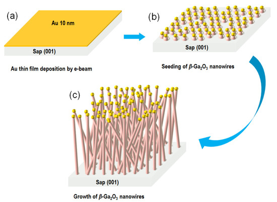
Figure 1.
Schematic diagram depicting growth process of single-crystal β-Ga2O3 nanowires on c-plane sapphire substrates by metalorganic chemical vapor deposition (MOCVD). (a) Au thin-film deposition. (b) Seeding of β-Ga2O3 nanowires. (c) Growth of β-Ga2O3 nanowires.
Before the root of β-Ga2O3 nanowires was grown, due to the surface tension effect, predeposited Au thin film self-assembled into nano islands that were randomly distributed all over the sapphire substrate as the reactor chamber temperature got higher, which could be used as catalysts in the growth of β-Ga2O3 nanowires on sapphire, with Au remaining in liquid form at this stage. [14,26] This could be apparently confirmed by the SEM images showing the growth process of β-Ga2O3 nanowires after 5 min and 30 min, as shown in Figure 2. The inset of Figure 2a clearly illustrates a β-Ga2O3 nanorod underneath an Au nanocrystal after 5 min growth. This growth process lasts as the nanowires get longer, while their diameters are highly consistent with the sizes of the Au nanocrystals, by which the growth direction selectivity and aspect ratio are greatly improved.
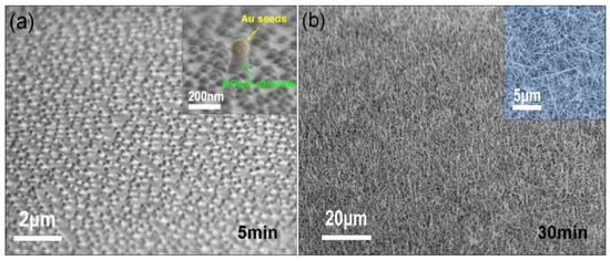
Figure 2.
Scanning electron microscopy (SEM) images illustrating the growth process of β-Ga2O3 nanowires (a) self-assembled Au nanocrystals as catalysts while sitting on β-Ga2O3 nanorods after 5 min growth; inset shows a close-up SEM image of a β-Ga2O3 nanorod under an Au nanocrystal after 5 min growth. (b) 45 degree tilted-view SEM image of β-Ga2O3 monoclinic nanowires after 30 min growth; inset is the bird-view SEM image of β-Ga2O3 nanowires after 30 min growth.
2.2. Characterization Methods
The growth process was monitored by taking the samples out of the MOCVD reactor to check the evolution of β-Ga2O3 nanowires with SEM. As the growth finished, the orientation of β-Ga2O3 nanowires were investigated by SEM (Hitachi S-4800), TEM (FEI Tecnai-G2-F20), Raman spectroscopy (HORIBA Scientific) and X-ray diffraction (Bede X-ray Metrology, 40 kV, λ: ~1.54 Å). A 532 nm green laser was used as the excitation source for the Raman test through an optical setup with an objective of 50×. In each scan, the integration time was set to be 5 min for collecting Raman signals from β-Ga2O3 nanowires. The energy band gap of β-Ga2O3 nanowires was estimated after a numerical fitting based on the transmittance spectrum using wideband light sources (200~800 nm) as the incidence. The transitions of excited carriers were analyzed to investigate the defects and their impact on the emission characteristics for β-Ga2O3 nanowires based on room temperature PL spectra. A 248 nm excimer laser was used as an optical pumping source and PL signals were collected by a prefocus lens and coupled into the entrance slit of a 500 mm spectrograph, dispersed by a 1200 L/mm grating to a cooled charged-coupled device (CCD), offering an optical resolution about 0.1 nm. As a comparison, a native β-Ga2O3 substrate was also included in the PL test.
3. Results and Discussion
An optical image in Figure 3a presents a quarter of a 2-inch sapphire wafer with β-Ga2O3 nanowires synthesized by MOCVD. Gray color of the wafer indicates that the nanowires are uniformly distributed on the sapphire substrate over a large area. These nanowires exhibit a nominal height of ~6.6 μm, as shown in the cross-sectional SEM image of β-Ga2O3 nanowires on sapphire in Figure 3b. A higher magnification SEM image in Figure 3c reveals the fairly vertically-oriented growth direction of β-Ga2O3 nanowires, with diameters ranging from ~50 nm to ~200 nm, indicating that the straight and long nanowires exhibit a very large aspect ratio. This is particularly true at the beginning of growth, as shown in the Figure 2b. In fact, the diameters of β-Ga2O3 nanowires are highly depended on the sizes of Au seeds before the growth, which suggests the feasibility to tune the size and density for as-grown β-Ga2O3 nanowires by depositing a thinner Au film for smaller and sparser Au nanoseeds. In addition, we can clearly observe that the spherical-shaped Au nanoparticles are sitting on the stem of the nanowire at the tips, which again confirms the growth mechanism as described before. The growth rate of nanowire in the vertical direction can be roughly estimated as 200 nm/min.
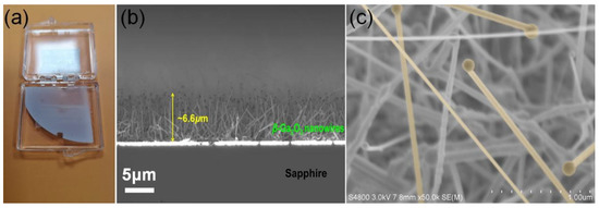
Figure 3.
(a) A quarter of 2-inch as-grown β-Ga2O3 nanowires on sapphire wafer. (b) Cross-sectional SEM image of the as-grown β-Ga2O3 nanowires. (c) High-magnification SEM image of nanowires.
Raman analysis was performed to analyze the crystal structure on typical β-Ga2O3 nanowire samples. It can be seen that strong and sharp Raman peaks from crystalline Ga\O bonds are centered at 200.1, 345.5, 476.9 and 417.3 cm−1 in Figure 4a. This spectrum demonstrates that the nanowires present the monoclinic β-Ga2O3 phase and have a very good crystal quality [27,28]. Meanwhile, XRD was used to examine the crystal structure of the large-area β-Ga2O3 nanowires grown by MOCVD. A typical XRD pattern of as-grown sample is shown in Figure 4b. The peaks at 21° and 41° correspond to the {0001} diffraction peaks of the sapphire substrate. In addition, three dominant diffraction peaks at 18.9°, 38.4° and 59.2° are observed, which correspond to the (01), (02), and (03) planes of β-Ga2O3, respectively. It illustrates that the β-Ga2O3 nanowires are mostly (01)-oriented, which is almost paralleled to the sapphire (0001) plane [29]. Three much weaker peaks correspond to the (201), (01), and (020) planes of β-Ga2O3. It again affirms that the as-grown vertically-oriented β-Ga2O3 nanowires have the monoclinic structure (β-Ga2O3 (a = 12.12–12.34, b = 3.03–3.04, c = 5.78–5.87)), according to the Joint Committee on Powder Diffraction Standards (JCPDS) powder diffraction file No. 76-0573. [29,30]. The growth temperature (690 °C) may contribute to the diffraction peaks of the α-phase Ga2O3 nanowires in Figure 4b [31].
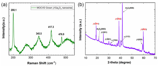
Figure 4.
(a) Raman and (b) X-ray diffraction (XRD) spectra of β-Ga2O3 nanowires.
In order to further investigate the detailed crystal structure of the as-grown sample, Figure 5a presents a typical TEM image of an individual synthesized β-Ga2O3 nanowire with a diameter of about 80 nm. The selected area electron diffraction (SAED) shown in the inset of Figure 5a confirms that the synthesized sample shows perfect crystallinity of monoclinic β-Ga2O3. Figure 5b presents a high resolution TEM (HRTEM) image of the β-Ga2O3 nanowires. The lattice fringes with a d spacing of 0.288 nm are observed, which corresponds to the (004) lattice planes of β-Ga2O3. The β-Ga2O3 nanowires of the same direction as the white arrow grow along the (01) direction, which is consistent with the results given in Figure 5a.
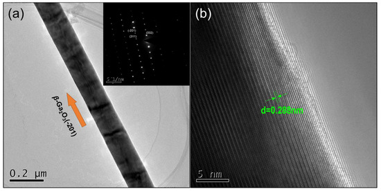
Figure 5.
(a) Transmission electron microscopy (TEM) image of an individual β-Ga2O3 nanowire. The typical electron diffraction pattern is in the inset. (b) High-resolution TEM image of the β-Ga2O3 nanowires with uniform lattice fringes.
Figure 6 presents the optical transmittance of the β-Ga2O3 nanowires. It can be clearly observed that the band-edge absorption for the as-grown β-Ga2O3 nanowires is at about 275 nm, from which the band gap can be roughly estimated as 4.53 eV by using the equation: Eg = 1240/λ. Moreover, it has a much lower absorption in the visible region when compared with the sharp band-edge absorption in the deep ultraviolet region below 280 nm, suggesting great potential for being used as solar-blind photodetectors for these nanowires. For a more accurate estimate, the optical band gap of the β-Ga2O3 nanowires is calculated by extrapolating the linear portion of the square of absorption coefficient against photon energy using the equation:
where α is absorption coefficient, h is the Planck’s constant, and υ is the frequency of the incident light, and B is a constant [7,32,33,34]. The band gap of β-Ga2O3 nanowires is estimated to be ~4.7 eV as shown in the inset of Figure 6. This value is in agreement with the band gaps from experiments ranging from 4.6 to 4.9 eV as reported by others [29]. It is also consistent with theoretical predictions of a direct band gap at Γ-point (Eg(Γ-Γ), ~4.8 ± 0.1 eV) and indirect band gap at L-point (Eg(Γ-L), ~4.7 ± 0.1 eV) by quasiparticle self-consistent GW calculations for β-Ga2O3 [35].
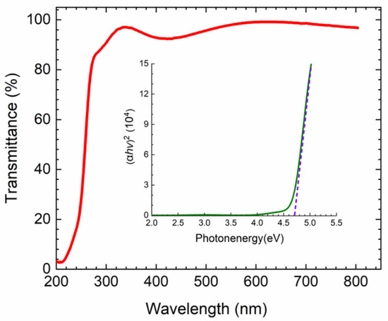
Figure 6.
Optical transmission spectrum of the β-Ga2O3 nanowires. (αhυ)2 versus photon energy plots of the β-Ga2O3 nanowires in the inset.
Figure 7 shows the PL spectrum obtained from β-Ga2O3 nanowires and native β-Ga2O3 (-201) substrate at room temperature at the same pumping conditions. For removing the artifacts from the laser sources, the PL spectrum from the nanowires is baseline-fitted. In the baseline fitting, to identify the intrinsic emission, the PL spectrum of nanowires is separated from the laser excitation background, as the intrinsic emissions of β-Ga2O3 is greatly overlapped with laser excitation background (see Figure 7). Emission spectral peaks centered at ~257 nm and ~275 nm can be observed, which correspond with the band-edge transitions of excited carriers that originate from the anisotropy of the monoclinic phase [36]. Aside from the band-edge emission, β-Ga2O3 nanowires exhibit two distinct spectral peaks at ~360 nm and ~410 nm, respectively, which are consistent with the PL spectral peaks of native β-Ga2O3 (-201) substrate. The peak at 360 nm is originated from recombination processes caused by self-trapped holes (STH), which is an intrinsic feature and is not due to defects. The spectral peak located at 410 nm is related to the recombination of donor–acceptor pairs (DAP), which is a result of electrons tunneling from the donor to the acceptor when photo-generated carriers are captured by donors or acceptors in β-Ga2O3. A weak spectral peak can be identified at ~440 nm for the β-Ga2O3 nanowires, corresponding to the blue band emission that strongly correlates with oxygen vacancy concentration [37]. Overall, the PL spectrum from β-Ga2O3 nanowires is highly consistent with that from native β-Ga2O3 substrate, which suggests high material quality of as-grown β-Ga2O3 nanowires.
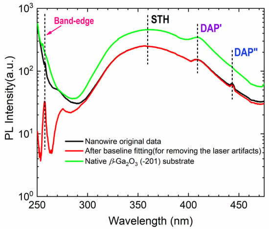
Figure 7.
Room temperature photoluminescence (PL) spectra of β-Ga2O3 nanowires and native β-Ga2O3 substrate at the same optical excitation conditions.
4. Conclusions
In summary, we have presented a new method to grow large-area single-crystal monoclinic β-Ga2O3 nanowires by MOCVD. Assisted by Au nanocrystal seeds as catalysts, the growth of nanowires exhibited a very good selectivity in the (01) direction, which demonstrates an array of >6 μm long one-dimensional nanowires. Diameters of the nanowires are highly depended on the sizes of Au nano particles, ranging from ~50 to ~200 nm. The room temperature PL spectrum obtained from β-Ga2O3 nanowires exhibits strong emissions centered at ~360 and ~410 nm, representing the recombination processes via electrons/self-trapped holes and donor–acceptor pairs, respectively, while the blue band emission was greatly suppressed with less O vacancies in β-Ga2O3 nanowires. The energy band gap of the β-Ga2O3 nanowires is estimated to be 4.7 eV according to the optical transmission test. Our method suggests a great potential in realizing controllable growth of β-Ga2O3 nanowires by predepositing highly-ordered Au nanoplates for arrayed growth. This work provides a new thought on the synthesis of high-quality β-Ga2O3 nanowires that facilitates the scaling down in the perspective of fabricating β-Ga2O3-based field-effect transistors and solar-blind photodetectors.
Author Contributions
Conceptualization, J.-H.P. and Y.Z.; formal analysis, C.J., J.-H.P. and Y.Z.; funding acquisition, Y.Z.; investigation, C.J., J.X., J.-H.P. and Y.Z.; methodology, J.-H.P. and Y.Z.; project administration, D.-W.J.; supervision, X.Y., J.-H.P. and Y.Z.; writing—original draft, C.J. and Y.Z.; writing—review and editing, J.-H.P. and Y.Z. All authors have read and agreed to the published version of the manuscript.
Funding
This research was funded by Chinese Academy of Sciences.
Acknowledgments
This research was supported by Basic Science Research Program through the National Research Foundation of Korea (NRF) funded by the Ministry of Education (No. 2018R1D1A1B07048429).
Conflicts of Interest
The authors declare no conflict of interest.
References
- Mazeina, L.; Picard, Y.N.; Maximenko, S.I.; Perkins, F.K.; Glaser, E.R.; Twigg, M.E.; Freitas, J.A.; Prokes, S.M. Growth of Sn-Doped β-Ga2O3 Nanowires and Ga2O3−SnO2 Heterostructures for Gas Sensing Applications. Cryst. Growth Des. 2009, 9, 4471–4479. [Google Scholar] [CrossRef]
- Kim, H.; Jin, C.; An, S.; Lee, C. Fabrication and CO Gas-sensing Properties of Pt-functionalized Ga2O3 Nanowires. Ceram. Int. 2012, 38, 3563–3567. [Google Scholar] [CrossRef]
- Higashiwaki, M.; Sasaki, K.; Kuramata, A.; Masui, T.; Yamakoshi, S. Development of Gallium Oxide Power Devices. Phys. Status Solidi A 2014, 211, 21–26. [Google Scholar] [CrossRef]
- Higashiwaki, M.; Kuramata, A.; Murakami, H.; Kumagai, Y. State-of-the-art Technologies of Gallium Oxide Power Devices. J. Phys. D: Appl. Phys. 2017, 50, 333002. [Google Scholar] [CrossRef]
- Feng, P.; Zhang, J.Y.; Li, Q.H.; Wang, T.H. Individual β-Ga2O3 nanowires as solar-blind photodetectors. Appl. Phys. Lett. 2006, 88, 153107. [Google Scholar] [CrossRef]
- Wang, S.; Sun, H.; Wang, Z.; Zeng, X.; Ungar, G.; Guo, D.; Shen, J.; Li, P.; Liu, A.; Li, C.; et al. In Situ Synthesis of Monoclinic β-Ga2O3 Nanowires on Flexible Substrate and Solar-blind Photodetector. J. Alloys Compd. 2019, 787, 133–139. [Google Scholar] [CrossRef]
- Chen, Y.-C.; Lu, Y.-J.; Liu, Q.; Lin, C.-N.; Guo, J.; Zang, J.-H.; Tian, Y.-Z.; Shan, C.-X. Ga2O3 Photodetector Arrays for Solar-blind Imaging. J. Mater. Chem. C 2019, 7, 2557–2562. [Google Scholar] [CrossRef]
- Wei, T.-C.; Tsai, D.-S.; Ravadgar, P.; Ke, J.-J.; Tsai, M.-L.; Lien, D.-H.; Huang, C.-Y.; Horng, R.-H.; He, J.-H. See-Through Ga2O3 Solar-Blind Photodetectors for Use in Harsh Environments. IEEE J. Select. Top. Quantum Electron. 2014, 20, 112–117. [Google Scholar] [CrossRef]
- Zhang, H.Z.; Kong, Y.C.; Wang, Y.Z.; Du, X.; Bai, Z.G.; Wang, J.J.; Yu, D.P.; Ding, Y.; Hang, Q.L.; Feng, S.Q. Ga2O3 Nanowires Prepared by Physical Evaporation. Solid State Commun. 1999, 109, 677–682. [Google Scholar] [CrossRef]
- Nogales, E.; García, J.Á.; Méndez, B.; Piqueras, J. Doped Gallium Oxide Nanowires with Waveguiding Behavior. Appl. Phys. Lett. 2007, 91, 133108. [Google Scholar] [CrossRef]
- Gonzalo, A.; Nogales, E.; Méndez, B.; Piqueras, J. Influence of Growth Temperature on the Morphology and Luminescence of Ga2O3:Mn Nanowires. Phys. Status Solidi A 2014, 211, 494–497. [Google Scholar] [CrossRef]
- Gonzalo, A.; Nogales, E.; Lorenz, K.; Víllora, E.G.; Shimamura, K.; Piqueras, J.; Méndez, B. Raman and Cathodoluminescence Analysis of Transition Metal Ion Implanted Ga2O3 Nanowires. J. Lumin. 2017, 191, 56–60. [Google Scholar] [CrossRef]
- Park, G.-S.; Choi, W.-B.; Kim, J.-M.; Choi, Y.C.; Lee, Y.H.; Lim, C.-B. Structural Investigation of Gallium Oxide (β-Ga2O3) Nanowires Grown by Arc-discharge. J. Cryst. Growth 2000, 220, 494–500. [Google Scholar] [CrossRef]
- Cha, S.Y.; Ahn, B.-G.; Kang, H.C.; Lee, S.Y.; Noh, D.Y. Direct Conversion of β-Ga2O3 Thin Films to β-Ga2O3 Nanowires by Annealing in a Hydrogen Atmosphere. Ceram. Int. 2018, 44, 16470–16474. [Google Scholar] [CrossRef]
- Chang, K.-W.; Wu, J.-J. Low-Temperature Growth of Well-Aligned β-Ga2O3 Nanowires from a Single-Source Organometallic Precursor. Adv. Mater. 2004, 16, 545–549. [Google Scholar] [CrossRef]
- Liang, C.H.; Meng, G.W.; Wang, G.Z.; Wang, Y.W.; Zhang, L.D.; Zhang, S.Y. Catalytic Synthesis and Photoluminescence of β-Ga2O3 Nanowires. Appl. Phys. Lett. 2001, 78, 3202–3204. [Google Scholar] [CrossRef]
- Sharma, S.; Sunkara, M.K. Direct Synthesis of Gallium Oxide Tubes, Nanowires, and Nanopaintbrushes. J. Am. Chem. Soc. 2002, 124, 12288–12293. [Google Scholar] [CrossRef]
- Chun, H.J.; Choi, Y.S.; Bae, S.Y.; Seo, H.W.; Hong, S.J.; Park, J.; Yang, H. Controlled Structure of Gallium Oxide Nanowires. J. Phys. Chem. B 2003, 107, 9042–9046. [Google Scholar] [CrossRef]
- Kumar, M.; Kumar, V.; Singh, R. Diameter Tuning of β-Ga2O3 Nanowires Using Chemical Vapor Deposition Technique. Nanoscale Res. Lett. 2017, 12, 184. [Google Scholar] [CrossRef]
- Ning, J.Q.; Xu, S.J.; Wang, P.W.; Song, Y.P.; Yu, D.P.; Shan, Y.Y.; Lee, S.T.; Yang, H. Microstructure and Micro-Raman Studies of Nitridation and Structure transition of Gallium Oxide Nanowires. Mater. Charact. 2012, 73, 153–157. [Google Scholar] [CrossRef]
- Kim, H.W.; Kim, N.H. Formation of Amorphous and Crystalline Gallium Oxide Nanowires by Metalorganic Chemical Vapor Deposition. Appl. Surf. Sci. 2004, 233, 294–298. [Google Scholar] [CrossRef]
- Kim, H.W.; Shim, S.H. Characteristics of Gallium Oxide Nanowires Synthesized by the Metalorganic Chemical Vapor Deposition. MSF 2007, 539–543, 1230–1235. [Google Scholar] [CrossRef]
- Kim, N.H.; Kim, H.W.; Seoul, C.; Lee, C. Amorphous Gallium Oxide Nanowires Synthesized by Metalorganic Chemical Vapor Deposition. Mater. Sci. Eng. B 2004, 111, 131–134. [Google Scholar] [CrossRef]
- Wu, X.C.; Song, W.H.; Huang, W.D.; Pu, M.H.; Zhao, B.; Sun, Y.P.; Du, J.J. Crystalline Gallium Oxide Nanowires: Intensive Blue Light Emitters. Chem. Phys. Lett. 2000, 328, 5–9. [Google Scholar] [CrossRef]
- Quan, Y.; Fang, D.; Zhang, X.; Liu, S.; Huang, K. Synthesis and Characterization of Gallium Oxide Nanowires via a Hydrothermal Method. Mater. Chem. Phys. 2010, 121, 142–146. [Google Scholar] [CrossRef]
- Sadan, H.; Kaplan, W.D. Au–Sapphire (0001) Solid–solid Interfacial Energy. J. Mater. Sci. 2006, 41, 5099–5107. [Google Scholar] [CrossRef]
- Rao, R.; Rao, A.M.; Xu, B.; Dong, J.; Sharma, S.; Sunkara, M.K. Blue Shifted Raman Scattering and Its Correlation with the [110] Growth Direction in Gallium Oxide Nanowires. J. Appl. Phys. 2005, 98, 94312. [Google Scholar] [CrossRef]
- Dohy, D.; Lucazeau, G.; Revcolevschi, A. Raman Spectra and Valence Force Field of Single-crystalline β-Ga2O3. J. Solid State Chem. 1982, 45, 180–192. [Google Scholar] [CrossRef]
- Nakagomi, S.; Kokubun, Y. Crystal Orientation of β-Ga2O3 Thin Films Formed on C-plane and A-plane Sapphire Substrate. J. Cryst. Growth 2012, 349, 12–18. [Google Scholar] [CrossRef]
- Pearton, S.J.; Yang, J.; Cary, P.H.; Ren, F.; Kim, J.; Tadjer, M.J.; Mastro, M.A. A Review of Ga2O3 Materials, Processing, and Devices. Appl. Phys. Rev. 2018, 5, 11301. [Google Scholar] [CrossRef]
- Oshima, T.; Okuno, T.; Fujita, S. Ga2O3 Thin Film Growth on c-Plane Sapphire Substrates by Molecular Beam Epitaxy for Deep-Ultraviolet Photodetectors. Jpn. J. Appl. Phys. 2007, 46, 7217–7220. [Google Scholar] [CrossRef]
- Zhang, Y.; Yan, J.; Li, Q.; Qu, C.; Zhang, L.; Xie, W. Optical and Structural Properties of Cu-doped β- Ga2O3 Films. Mat. Sci. Eng. B 2011, 176, 846–849. [Google Scholar] [CrossRef]
- Liu, Q.; Guo, D.; Chen, K.; Su, Y.; Wang, S.; Li, P.; Tang, W. Stabilizing the Metastable γ Phase in Ga2O3 Thin Films by Cu Doping. J. Alloys Compd. 2018, 731, 1225–1229. [Google Scholar] [CrossRef]
- Huang, L.; Feng, Q.; Han, G.; Li, F.; Li, X.; Fang, L.; Xing, X.; Zhang, J.; Hao, Y. Comparison Study of β-Ga2O3 Photodetectors Grown on Sapphire at Different Oxygen Pressures. IEEE Photonics J. 2017, 9, 1–8. [Google Scholar] [CrossRef]
- Ratnaparkhe, A.; Lambrecht, W.R.L. Quasiparticle Self-consistent GW Band Structure of β -Ga 2 O 3 and the Anisotropy of the Absorption Onset. Appl. Phys. Lett. 2017, 110, 132103. [Google Scholar] [CrossRef]
- Li, Y.; Tokizono, T.; Liao, M.; Zhong, M.; Koide, Y.; Yamada, I.; Delaunay, J.-J. Efficient Assembly of Bridged β-Ga2O3 Nanowires for Solar-Blind Photodetection. Adv. Funct. Mater. 2010, 20, 3972–3978. [Google Scholar] [CrossRef]
- McCluskey, M.D. Point Defects in Ga2O3. J. Appl. Phys. 2020, 127, 101101. [Google Scholar] [CrossRef]
© 2020 by the authors. Licensee MDPI, Basel, Switzerland. This article is an open access article distributed under the terms and conditions of the Creative Commons Attribution (CC BY) license (http://creativecommons.org/licenses/by/4.0/).


