Article

Low-Temperature Processed TiOx Electron Transport Layer for Efficient Planar Perovskite Solar Cells

1
Nanomaterials Research Institute, Kanazawa University, Kakuma, Kanazawa 920-1192, Japan
2
Graduate School of Natural Science and Technology, Kanazawa University, Kakuma, Kanazawa 920-1192, Japan
3
Graduate School of Frontier Science Initiative, Kanazawa University, Kakuma, Kanazawa 920-1192, Japan
4
Department of Physics, Engineering Physics and Astronomy, Queen’s University, Kingston, ON K7L 3N6, Canada
*
Authors to whom correspondence should be addressed.
Nanomaterials 2020, 10(9), 1676; https://doi.org/10.3390/nano10091676
Submission received: 23 July 2020 / Revised: 21 August 2020 / Accepted: 23 August 2020 / Published: 26 August 2020
(This article belongs to the Special Issue Mesoporous Materials and Nanoscale Phenomena in Hybrid Photovoltaics)

Abstract

:
The most frequently used n-type electron transport layer (ETL) in high-efficiency perovskite solar cells (PSCs) is based on titanium oxide (TiO2) films, involving a high-temperature sintering (>450 °C) process. In this work, a dense, uniform, and pinhole-free compact titanium dioxide (TiOx) film was prepared via a facile chemical bath deposition process at a low temperature (80 °C), and was applied as a high-quality ETL for efficient planar PSCs. We tested and compared as-deposited substrates sintered at low temperatures (< 150 °C) and high temperatures (> 450 °C), as well as their corresponding photovoltaic properties. PSCs with a high-temperature treated TiO2 compact layer (CL) exhibited power conversion efficiencies (PCEs) as high as 15.50%, which was close to those of PSCs with low-temperature treated TiOx (14.51%). This indicates that low-temperature treated TiOx can be a potential ETL candidate for planar PSCs. In summary, this work reports on the fabrication of low-temperature processed PSCs, and can be of interest for the design and fabrication of future low-cost and flexible solar modules.

Graphical Abstract

1. Introduction

Solid-state organic–inorganic hybrid perovskite solar cells (PSCs) have been one of the most significant discoveries in the field of photovoltaics because of their advantages, including a low-cost device fabrication process, desirable energy harvesting characteristics, light weight, and flexibility [1,2,3,4]. The first report of PSCs with a power conversation efficiency (PCE) of 3.8% was by Miyasaka et al. in 2009 [5]. Intensive research efforts have subsequently been undertaken on PSCs, with a reported record PCE of 25.2% under laboratory conditions [6]. In conventional PSC architecture, a perovskite film is sandwiched in between an electron transport layer (ETL) and a hole transport layer (HTL), and both layers are also sandwiched between a transparent electrode and a metal electrode in order to fabricate complete devices. In terms of improving PSC performance, it is significantly important to produce a uniform, compact, pinhole-free, and full surface coverage titanium oxide (TiO2) compact layer (CL) as the ETL in order to achieve more efficient electron transport, charge extraction, and low interfacial recombination [7]. PSCs can be fabricated entirely using low-cost solution processing [8] and vacuum deposition methods [9,10]. The high stability and efficiency of PSCs with low-cost processing can enable the realization of economically competitive solar power. In general, there are two leading device configurations for PSCs: planar heterojunction (PHJ) and mesoporous scaffold-based devices [11,12,13]. Thin ETLs serve a key function of extracting electrons from the perovskite layer, and blocking recombination between electrons in the fluorine-doped tin oxide (FTO) and holes in the perovskite layer. A thick ETL can minimize recombination; however, the electron flow may be limited because of high series resistance. Very few PSC structures have been fabricated without an ETL, and they generally have low PCEs compared with PHJ PSCs prepared with an ETL [14,15]. High-quality mesoporous TiO2 scaffold films and TiO2 CL require a high-temperature sintering (> 450 °C) step, which limits their applications in future flexible PSCs and solar modules. The active surface area and performance of the devices was improved by forming the perovskite layer on a layer composed of TiO2 CL/TiO2 nanoparticles [16,17,18]. The development of PHJ PSCs with low-temperature processed (< 150 °C) ETL CLs has attracted significant attention for their simple device framework [19].
Several groups have developed ETLs using a TiO2 CL with different deposition techniques, including spin coating [20], spray pyrolysis [21,22,23], oblique electrostatic inkjet [24], electrodeposition [25], inkjet printing [26], atomic layer deposition [27], sputtering [28], and chemical bath deposition (CBD) [29] for PSC applications. Notable ETLs can be fabricated using either spin coating or spray pyrolysis top-down techniques, although these are quite sensitive to the control parameters, and subsequently the PCE of such fabricated devices may vary considerably. Alberti et al. reported a low-temperature nanostructured TiO2 layer via reactive sputtering, with a maximum PCE of ∼15% without surface treatments or additional layers [28]. Sputtering demands a vacuum environment and has a slow deposition rate that presents challenges for producing TiO2 films. However, unlike other bottom-up techniques, the CBD technique is an encouraging candidate for producing TiO2 CLs using a low-cost fabrication process that is compatible with large-scale fabrication. The CBD technique produces high-quality TiO2 CLs, which can be used as the ETL in PSCs. However, Takahashi and coworkers [30] developed a simple, low-cost, uniform, air-stable, scalable CBD technique that was followed by low-temperature thermal annealing (< 150 °C) in order to deposit titanium dioxide (TiOx) CLs with controlled film thicknesses for the deposition of the ETL in organic solar cells. In addition, Chen and coworkers reported a relatively low-temperature processed flower-like TiO2 ETL-based PSC with a PCE of 15.71% [31]. Furthermore, Liu et al. [32] prepared Nb-doped TiO2 via a CBD, and achieved a PCE as high as 19.23%. However, a fundamental understanding of the CBD growth of the TiO2 films has not been studied in depth in order to realize their full potential. Therefore, it is important to develop PHJ PSCs with low-temperature processed (< 150 °C) CBD–TiOx CL ETLs in order to have the possibility of fabricating cost-effective solar modules. Moreover, low-temperature processing is mandatory for the development of flexible solar cells and modules [33,34].
In this study, we used a simple, low-temperature, scalable CBD process to fabricate a uniform, pinhole free, and air stable amorphous TiOx film. We investigated and compared the formation of compact TiOx processed at a low temperature (< 150 °C) and compact TiO2 treated at a high temperature (> 450 °C) as ETLs, as well as their corresponding solar cell properties. While there was a difference in crystallinity between the TiOx and TiO2 films, no difference was observed in the chemical bonding states and surface morphology. In addition, the perovskite films formed on the TiOx and TiO2 films had similar crystallinities and surface morphologies, and their device performances were comparable.

2. Materials and Methods

2.1. Materials

All of the commercially available materials were purchased and used as received, without further purification. Fluorine-doped tin oxide (FTO) and indium tin oxide (ITO)-patterned glass substrates were purchased from Asahi Glass (Tokyo, Japan). Lead iodide (PbI2; purity 98%) and methylammonium iodide (CH3NH3I; purity 98%) were purchased from Tokyo Chemical Industry (Tokyo, Japan). Titanium (IV) oxysulfate (TiOSO4; purity 99.99%) was purchased from Sigma Aldrich (St. Louis, MO, USA). Hydrogen peroxide (H2O2; purity 35%) and N, N-dimethylformamide (DMF; purity 99.5%) were supplied by Kanto Chemical (Tokyo, Japan).

2.2. Device Fabrication

FTO- and ITO-patterned glass substrates were sequentially cleaned in a sonication bath with a KOH solution (1.4 g of KOH dissolved in 50 mL of ultrapure water) followed by ultrapure water for 10 min each for two cycles. The cleaned FTO and ITO substrates were then dried with nitrogen flow and pre-treated using oxygen plasma for 20 min prior to use. A complex precursor solution was prepared by adding water as a solvent, TiOSO4 as a titanium source, and H2O2 as a complexing agent, followed by heating, and was deposited on FTO or ITO substrates, according to the procedure described by Kuwabara et al. [30]. Then, the as-deposited substrates were baked at a low temperature (<150 °C) for 1 h and at a high temperature (> 450 °C) for 30 min. Then, 0.482 g of PbI2 and 0.168 g of CH3NH3I were dissolved and mixed in anhydrous DMF (652 µL):DMSO (163 µL) at a ratio of 4:1. The perovskite precursor solution was stirred at 70 °C for 60 min prior to spin coating. A perovskite precursor solution was spin-coated in three steps, as follows: first step, 0 rpm for 10 s; second step, 1000 rpm for 10 s; and third step, 5000 rpm for 30 s. In the third step, 400 µL of chlorobenzene solvent was dripped on the substrate 5 s before the end of spin-coating, and was transferred to a hot plate at 100 °C for 60 min in a glove box under an inert environment and then cooled to room temperature. The Spiro-OMeTAD solution, used as the hole transport layer, was prepared according to the report by Wakamiya et al. [35]. Finally, a gold (Au) electrode with a thickness of 100 nm was deposited at a 1.0 Å/s growth rate on the Spiro-OMeTAD layer so as to complete the device.

2.3. Characterization

Scanning electron microscopy (SEMSU1510, Hitachi High-Tech, Tokyo, Japan) together with atomic force microscopy (AFM; SII SPI3800N, Seiko, Japan) were used to analyze the surface morphology. The X-ray diffraction (XRD) patterns of the prepared films were measured using an X-ray diffractometer (SmartLab, Rigaku, Japan) with an X-ray tube (Cu Kα radiation, λ = 1.5406 Å). Surfcorder (ET 200, Tokyo, Japan) was used to measure the thickness of the films. The current density versus voltage (J–V) characteristics of all of the fabricated PSCs were measured at a scan rate of 0.05 V/s in forward scan (FS; from −0.2 to 1.2 V) and reverse scan (RS; from 1.2 to −0.2 V) directions. Each device had a 0.09 cm2 active area. Measurements were obtained under 100 mW/cm2 AM 1.5G irradiation from a solar simulator, and were measured using a Keithley 2401 digital source meter. The incident photon-to-conversion efficiency (IPCE) spectrum of each device was measured using a monochromatic xenon arc light system (Bunkoukeiki, SMI-250JA, Tokyo, Japan).

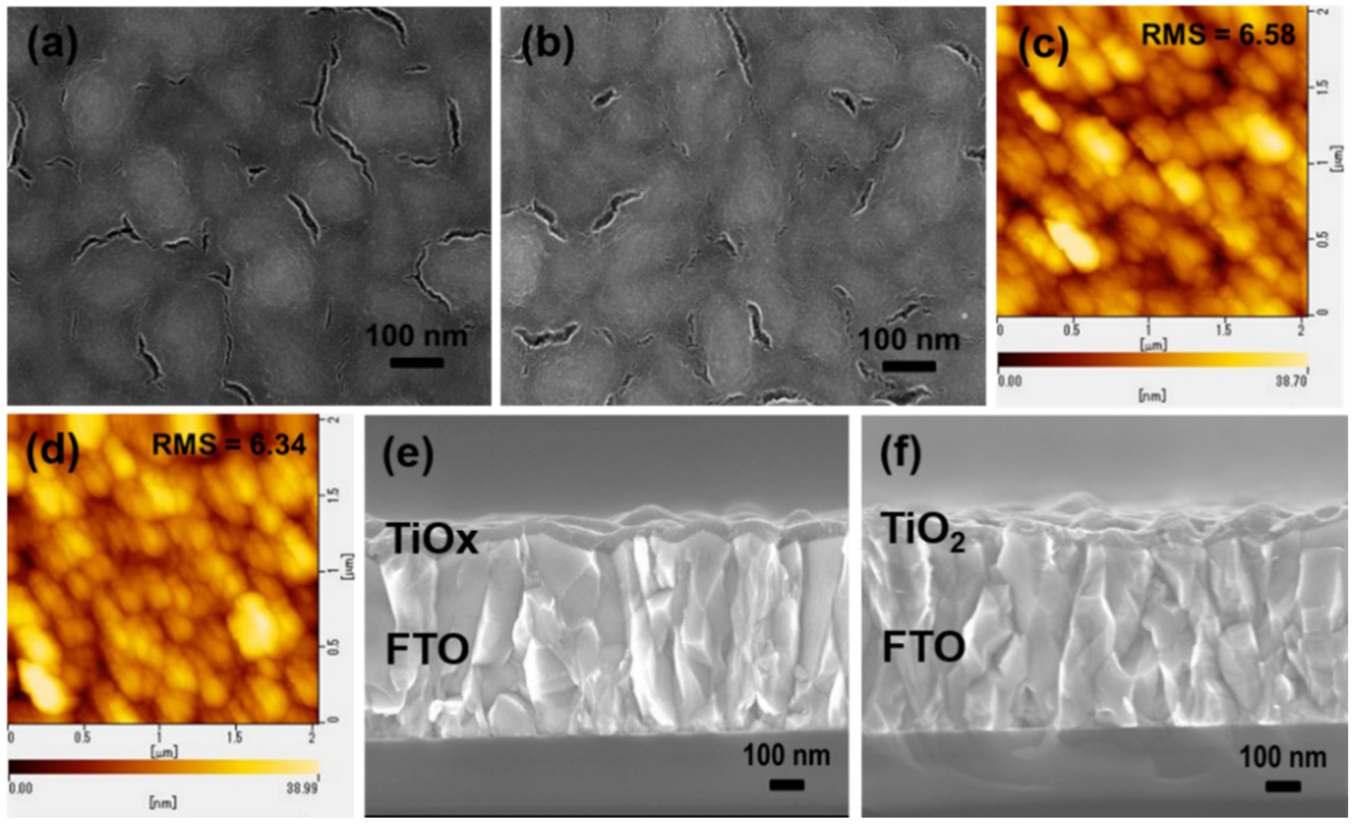
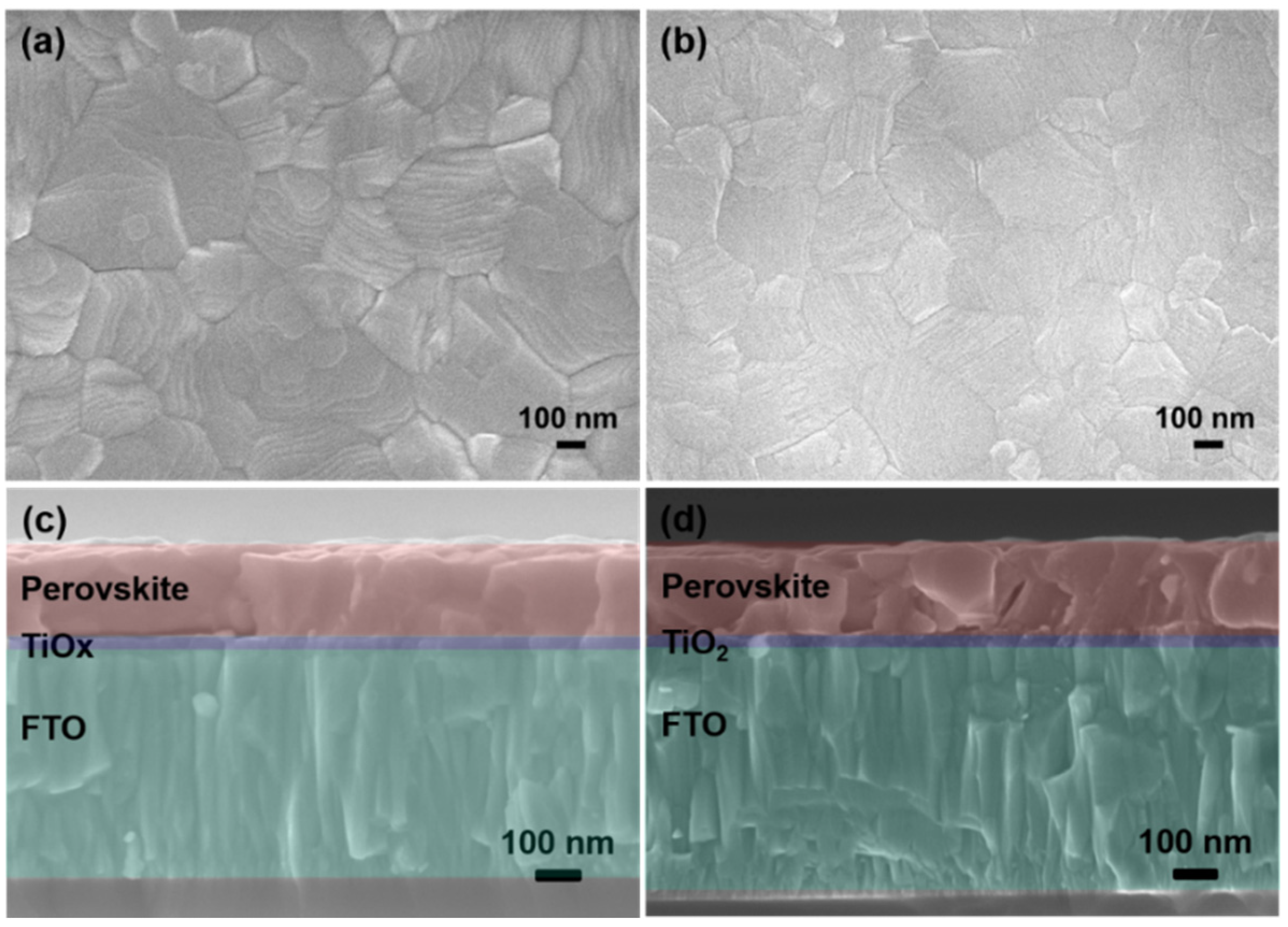
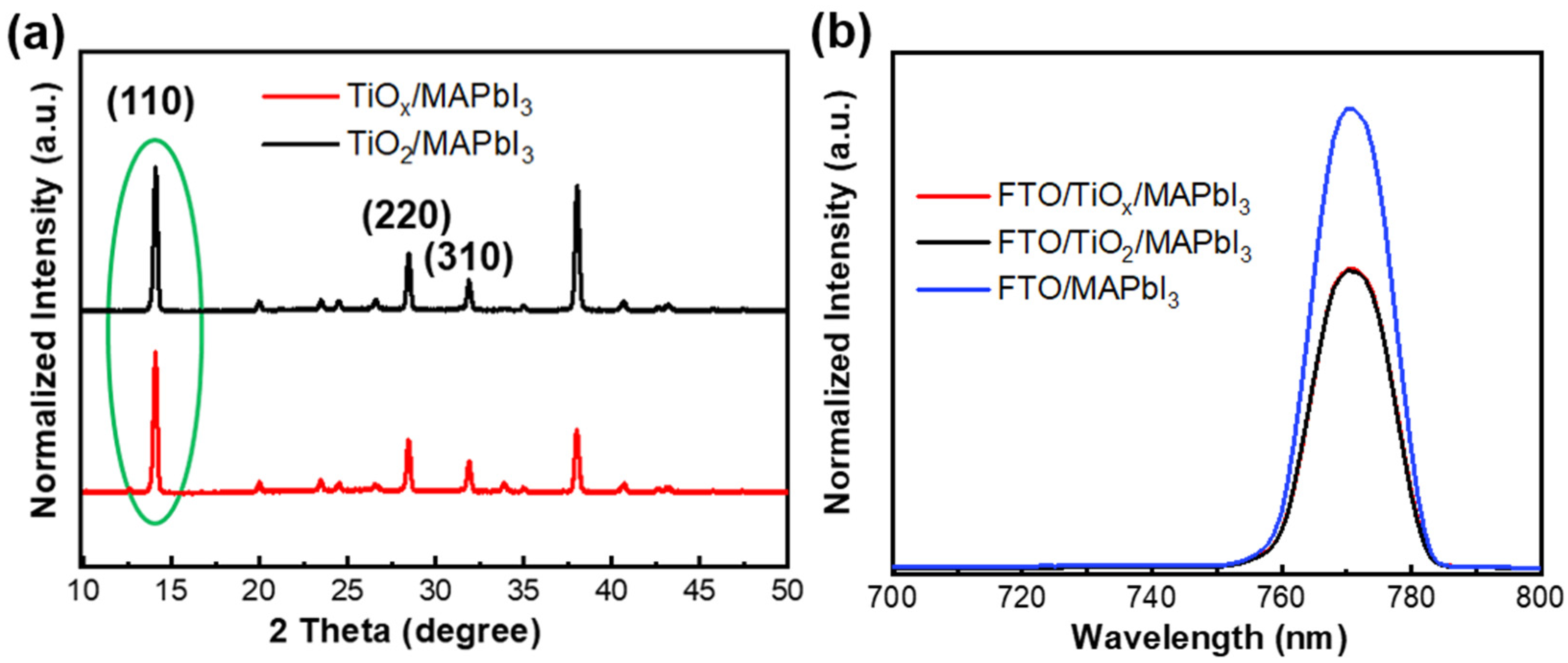
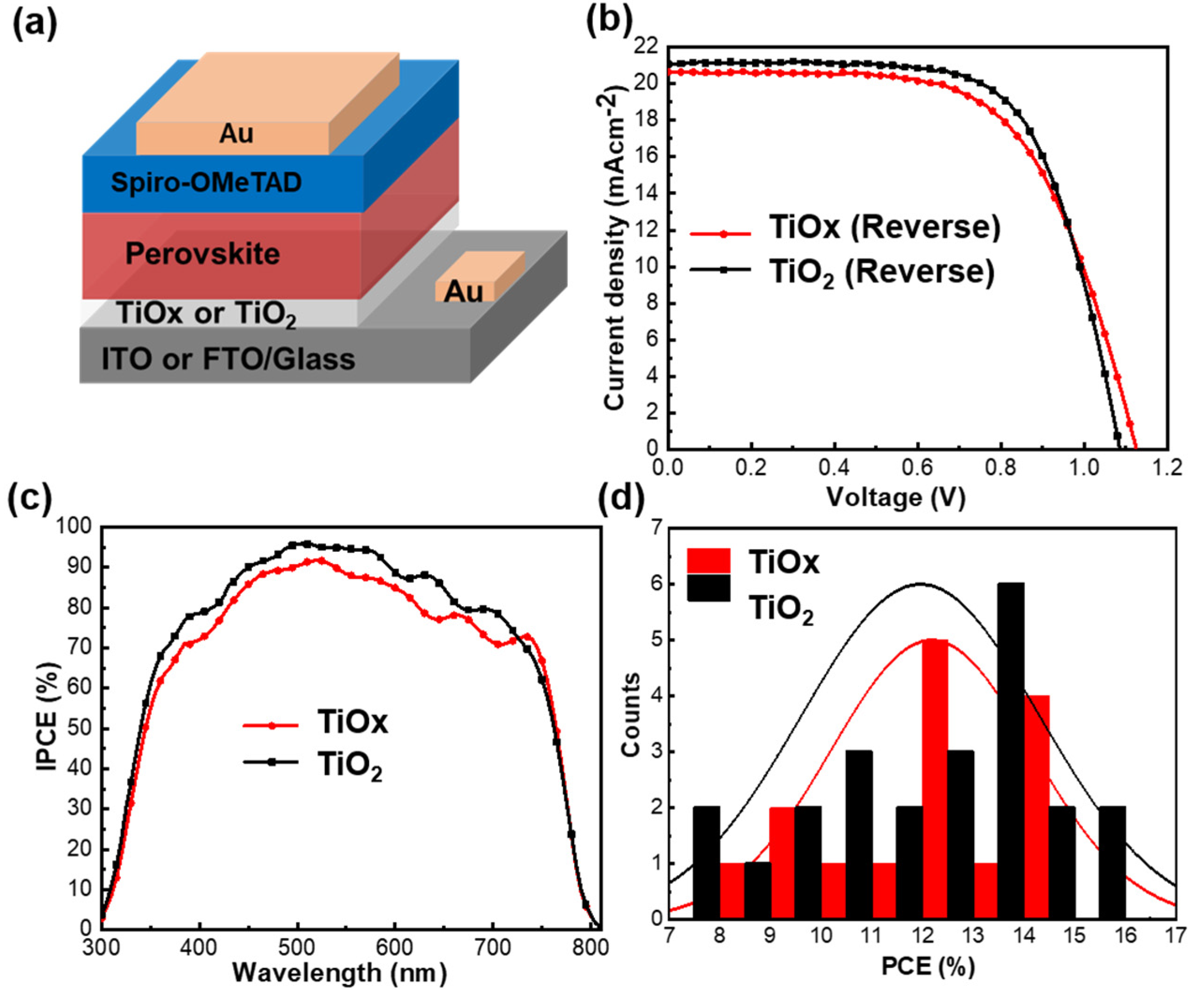
3. Results and Discussion

Figure 1a shows a schematic of the facile chemical bath deposition process at a low temperature (80 °C) for fabrication of the TiOx films, as well as their corresponding thermal treatments at 150 °C for 1 h and 450 °C for 30 min. Figure 1b,c shows the XPS spectra of the TiOx and TiO2 films. The Ti2p peak positions were unchanged for both the low-temperature processed TiOx and high-temperature treated TiO2 films, indicating that the TiOx showed the same chemical bonding state as TiO2 (Figure 1c). In addition, from the XPS spectrum, the peak intensity of TiO2 O1s O–Ti and Ti2p3/2 increased compared with TiOx, as shown in Figure 1b,c. This peak can be attributed to the high crystallinity of the TiO2 film; the high-temperature treated TiO2 retained its crystallinity, while the low-temperature TiOx had an amorphous structure (Figure S1). The obtained Raman spectra further confirmed these results. A peak for the anatase crystal structure of the TiO2 film was confirmed at ~150 cm−1, while no peak (black line) was found in the TiOx film (Figure 1d). This observation is similar to those previously reported by Sangaletti et al. [36]. Therefore, it can be inferred that the bond strength of TiO2 changed because of the crystallinity.
Water droplets on the TiOx and TiO2 films are shown in Figure 1e,f. The TiOx film shows a higher water contact angle of 36.7°, while the TiO2 film exhibits a lower contact angle of 6.6°, indicating that the TiOx film had a lower wettability compared with the TiO2 film. The superior wettability of the TiO2 film may be another avenue to improve the PCE of the resulting PSCs (as discussed later). In addition, we performed contact angle measurements to evaluate the surface-free energy of the TiOx and TiO2 films. The contact angles at three different points on each film surface with water, formamide, and ethylene glycol were obtained and the average values were used to calculate the surface-free energy of each film [37]. The surface-free energy of the TiOx and TiO2 films was 56.9 mJm−2 and 51.8 mJm−2, respectively, suggesting that a lower surface-free energy facilitates the formation of a more stable film surface. Therefore, it can be concluded that the surface state of the high-temperature treated TiO2 film affords a higher stability than the low-temperature treated TiOx film.
Top-view SEM images of the TiOx and TiO2 films are shown in Figure 2a,b. It can be seen that almost similar surface morphologies that are uniform, dense, and pinhole free on an FTO substrate were obtained with both films. These smooth, pinhole-free, and dense scaffolds may offer efficient charge extraction and hole blocking in the resulting PSCs. This was further confirmed via atomic force microscopy (AFM) analysis, as shown in Figure 2c,d. The root mean square (RMS) roughness for the TiOx and TiO2 films was 6.58 and 6.34 nm, respectively, indicating that the film surface roughness was nearly equivalent in both cases. It can be concluded for both samples that the surface morphology and roughness showed similar trends, regardless of the crystallinity. Cross-sectional SEM images of the TiOx and TiO2 films are shown in Figure 2e,f. Both samples clearly show smooth films deposited (60 nm thickness) on the FTO substrates, which efficiently blocked direct contact between the FTO and perovskites. This implies that low-temperature treated TiOx solely serves as a potential ETL candidate for planar PSCs.
Figure 3a,b shows the top-view SEM images of the TiOx/MAPbI3 and TiO2/MAPbI3 films. It can be seen that both samples had large crystal grains with a uniform and flat surface morphology. The film with a smooth surface morphology and large perovskite grains has fewer grain boundaries and fewer traps, which aids in reducing the charge carrier losses at the trap states in the grain boundaries [38]. We compared the cross-sectional SEM images of the TiOx- and TiO2-based PSCs, as shown in Figure 3c,d, respectively. Both samples had perovskite films with similar thicknesses of 300 nm.
The XRD patterns of the TiOx/MAPbI3 and TiO2/MAPbI3 films are shown in Figure 4a,b. Diffraction peaks were detected at 2θ angles of 14.1°, 28.5°, and 31.8° in the TiOx/MAPbI3 and TiO2/MAPbI3 perovskite films, and the peaks were assigned to the (110), (220), and (310) crystal planes, respectively. There was no peak from PbI2 at 12.6° for both samples, indicating the complete transformation of PbI2. The full width at half maximum (FWHM) of the TiOx/MAPbI3 and TiO2/MAPbI3 films was 0.246 and 0.247, respectively, suggesting a similar crystallinity for the perovskite films, despite the difference in crystallinity for their respective ETLs [39]. The photoluminescence (PL) spectra of the FTO/MAPbI3, FTO/TiOx/MAPbI3, and FTO/TiO2/MAPbI3 films were measured and the results are shown in Figure 4b. The peak intensity was lower, in addition to an increased PL quenching compared with the perovskite formed on the FTO substrate, which confirms that efficient charge extraction occurred from the perovskite film. When the perovskite films were formed on TiOx and TiO2, a similar PL quenching was obtained for both samples, which implied efficient electron transfer from the perovskite film to the ETLs. This suggests that the TiOx and TiO2 films have similar charge extraction capabilities [40,41].
We carried out electrochemical impedance spectroscopy (EIS) to further investigate the electrical properties of each interface, including the charge transfer, carrier recombination, and inner series resistance. Figure 5 shows Nyquist plots of the TiOx- and TiO2-based devices at zero bias in the dark and under AM 1.5G–100 mW/cm2 simulated sunlight irradiation. According to the equivalent circuit model shown in the Figure 5a inset, detailed Nyquist plots fitting the analysis parameters of the corresponding devices are summarized in Table S1. R1 can be considered a resistance component derived from the ETL, while R2 is termed as a resistance component derived from the interface between the ETL and perovskite. R1 is a resistance component derived from the ETL and is labeled as charge transferred resistance (RCT). The reduction in RCT contributed to the superior charge transfer in the TiO2-based device compared with the TiOx-based device, implying that a difference in the crystallinity of TiO2 may contribute to charge transfer at the interface. In addition, R2 is a resistance component at the interface and is considered to be a charge recombination resistance. The larger value contributed to a lower recombination at the interfaces. Mostly equivalent values were obtained for both devices for R2, which is consistent with the results from the corresponding PL spectra (Figure 4b).
Figure 6a shows the complete device structure. The current density versus voltage (J–V) characteristics under 1 sun AM 1.5G (100 mW/cm2) for the TiOx- and TiO2-based PSCs are shown in Figure 6b. The corresponding device parameters are summarized in Table 1. A comparison of the scan direction for the FS and RS is provided in Table S2. The PSC with the TiOx film exhibited a short circuit current density (Jsc) of 20.64 mAcm−2, open-circuit voltage (Voc) of 1.12 V, fill factor (FF) of 0.63, and PCE of 14.51% in the RS direction. The PSC with the TiO2 film had a Jsc of 21.06 mAcm−2, Voc of 1.08, FF of 0.68, and PCE of 15.50% in the RS direction. The enhancement of Jsc and FF was attributed to a lowering of the injection barrier at the interface between the TiO2 CL and perovskite; this is because the high-temperature treated TiO2 CL formed a smooth interface (Figure 1e), which facilitated efficient electron flow. The enhancement of Voc was unclear for the TiOx-based PSCs compared with the TiO2-based PSCs. Additionally, large hysteresis was observed in the J–V curves for both devices (Figure S2a). Previous reports have demonstrated a similar hysteresis behavior for TiO2 CL-based PSCs because of the rough interface between the TiO2 and perovskite [42]. The PSC with TiO2 CL as the ETL exhibited a PCE as high as 15.50%, which is close to that of the PSC with the TiOx ETL (14.51%). This implies that thermal annealing at a high temperature is not necessary in order to achieve high-performance PSCs. The incident photon-to-conversion efficiency (IPCE) was measured in order to verify the reproducibility of the PSCs based on the TiOx and TiO2 films, as shown in Figure 6c. The PSCs with TiOx and TiO2 films produced integrated photocurrents of 19.1 and 20.02 mAcm−2, respectively. The IPCE value of the TiO2-based PSC was slightly higher than that of the TiOx-based PSC over the same wavelength range, indicating that the electrons were efficiently collected at the interface between the TiO2 CL and perovskite, along with a reduction in the interfacial energy barrier. A histogram of the device PCEs for both the TiOx- and TiO2-based devices is shown in Figure 6d. The PCE distributions for both devices were nearly similar, implying that a low-temperature processed TiOx film can be used as an efficient ETL in future flexible solar modules.
To verify the reproducibility of the devices based on the TiOx and TiO2 films, we compared the average Jsc, Voc, FF, and PCE values of 18 and 26 individual devices, respectively, as shown in Figure 7. Reproducibility is one of the most important parameters for modularization. The low-temperature treated TiOx and high-temperature treated TiO2 samples showed similar reproducibility results. This indicated that low-temperature treated TiOx performs as well as the high-temperature treated TiO2 in PSCs. Furthermore, we investigated the effectiveness of the low-temperature (< 150 °C) processed TiOx on an ITO substrate, which exhibited a satisfactory photovoltaic performance compared with the FTO substrate (Figure S2b). The corresponding PSC parameters are summarized in Table S3. It can be concluded that a similar trend was observed for the low-temperature treated TiOx on an ITO substrate device. Therefore, the results show that the low-temperature treated TiOx film had a beneficial contribution to the PSC devices, which could help in further lowering the cost of the module manufacturing process in the future.

4. Conclusions

In this work, we fabricated and compared as-deposited substrates with TiOx and TiO2 films sintered at low temperatures (< 150 °C) and high temperatures (> 450 °C), and investigated their corresponding photovoltaic properties. The TiOx-based PSCs exhibited a satisfactory photovoltaic performance compared with the TiO2-based PSCs. The PSC with a TiOx CL showed a PCE of 14.51%, which was very close to that of the TiO2 CL-based PSCs (15.50%). In addition, a similar reproducibility was observed for devices fabricated using the TiOx and TiO2 films. This suggests that TiOx CL serves as a potential ETL in the PSC. There was a difference in crystallinity between the TiOx and TiO2 films, while the chemical bonding states and surface morphology were similar. Furthermore, there was no difference between the perovskite films grown on TiOx and TiO2 films, and an almost similar device performance was achieved. This work can enable the fabrication of entirely low-temperature processed PSCs, and could possibly contribute to the fabrication of flexible solar modules in the future.

Supplementary Materials

The following are available online at https://www.mdpi.com/2079-4991/10/9/1676/s1: Figure S1: XRD pattern of low-temperature treated TiOx film on an FTO substrate; Figure S2: Forward scan and reverse scan J–V curves of (a) TiOx and TiO2 films deposited on an FTO substrate; (b) TiOx film grown on an ITO substrate; Table S1: Nyquist plots fitting the analysis parameters; Table S2: Summary of device performance characteristics with TiOx- and TiO2-based PSCs; Table S3: Summary of device performance characteristics with a TiOx film deposited on an ITO substrate-based PSC.

Author Contributions

Conceived the idea, designed the experiments, wrote the original draft manuscript, and drew the figures, M.S.; conducted the experiment on perovskite devices, D.K.; reviewed the manuscript and discussed the results, M.S., M.N., M.K., K.T., J.-M.N., and T.T.; visualization, J.-M.N., and T.T.; supervised the whole study, T.T. All authors have read and agreed to the published version of the manuscript.

Funding

This research received no external funding.

Acknowledgments

This study was supported by the Grant-in-Aid for Scientific Research, grant number 20H02838, for financial support.

Conflicts of Interest

The authors declare no conflict of interest.

References

  1. Stranks, S.D.; Eperon, G.E.; Grancini, G.; Menelaou, C.; Alcocer, M.J.P.; Leijtens, T.; Herz, L.M.; Petrozza, A.; Snaith, H.J. Electron-Hole Diffusion Lengths Exceeding 1 Micrometer in an Organometal Trihalide Perovskite Absorber. Science 2013, 342, 341–344. [Google Scholar] [CrossRef] [PubMed] [Green Version]
  2. Noh, J.H.; Im, S.H.; Heo, J.H.; Mandal, T.N.; Seok, S.I. Chemical Management for Colorful, Efficient, and Stable Inorganic–Organic Hybrid Nanostructured Solar Cells. Nano Lett. 2013, 13, 1764–1769. [Google Scholar] [CrossRef] [PubMed]
  3. Jena, A.K.; Kulkarni, A.; Miyasaka, T. Halide Perovskite Photovoltaics: Background, Status, and Future Prospects. Chem. Rev. 2019, 119, 3036–3103. [Google Scholar] [CrossRef] [PubMed]
  4. Shahiduzzaman, M.; Fukaya, S.; Muslih, E.Y.; Wang, L.; Nakano, M.; Akhtaruzzaman, M.; Karakawa, M.; Takahashi, K.; Nunzi, J.-M.; Taima, T. Metal Oxide Compact Electron Transport Layer Modification for Efficient and Stable Perovskite Solar Cells. Materials 2020, 13, 2207. [Google Scholar] [CrossRef]
  5. Kojima, A.; Teshima, K.; Shirai, Y.; Miyasaka, T. Organometal Halide Perovskites as Visible-Light Sensitizers for Photovoltaic Cells. J. Am. Chem. Soc. 2009, 131, 6050–6051. [Google Scholar] [CrossRef]
  6. Best Research-Cell Efficiency Chart. Available online: https://www.nrel.gov/pv/cell-efficiency.html (accessed on 24 May 2020).
  7. Shalan, A.E.; Narra, S.; Oshikiri, T.; Ueno, K.; Shi, X.; Wu, H.-P.; Elshanawany Mahmoud, M.; Wei-Guang Diau, E.; Misawa, H. Optimization of a compact layer of TiO2 via atomic-layer deposition for high-performance perovskite solar cells. Sustain. Energy Fuels 2017, 1, 1533–1540. [Google Scholar] [CrossRef] [Green Version]
  8. Shahiduzzaman, M.; Visal, S.; Kuniyoshi, M.; Kaneko, T.; Umezu, S.; Katsumata, T.; Iwamori, S.; Kakihana, M.; Taima, T.; Isomura, M.; et al. Low-Temperature-Processed Brookite-Based TiO2 Heterophase Junction Enhances Performance of Planar Perovskite Solar Cells. Nano Lett. 2019, 19, 598–604. [Google Scholar] [CrossRef]
  9. Liu, M.; Johnston, M.B.; Snaith, H.J. Efficient planar heterojunction perovskite solar cells by vapour deposition. Nature 2013, 501, 395–398. [Google Scholar] [CrossRef]
  10. Shahiduzzaman, M.; Yonezawa, K.; Yamamoto, K.; Ripolles, T.S.; Karakawa, M.; Kuwabara, T.; Takahashi, K.; Hayase, S.; Taima, T. Improved Reproducibility and Intercalation Control of Efficient Planar Inorganic Perovskite Solar Cells by Simple Alternate Vacuum Deposition of PbI2 and CsI. ACS Omega 2017, 2, 4464–4469. [Google Scholar] [CrossRef] [Green Version]
  11. Chen, Q.; Zhou, H.; Hong, Z.; Luo, S.; Duan, H.-S.; Wang, H.-H.; Liu, Y.; Li, G.; Yang, Y. Planar Heterojunction Perovskite Solar Cells via Vapor-Assisted Solution Process. J. Am. Chem. Soc. 2014, 136, 622–625. [Google Scholar] [CrossRef]
  12. Yang, W.S.; Noh, J.H.; Jeon, N.J.; Kim, Y.C.; Ryu, S.; Seo, J.; Seok, S.I. High-Performance photovoltaic perovskite layers fabricated through intramolecular exchange. Science 2015, 348, 1234–1237. [Google Scholar] [CrossRef] [PubMed]
  13. Shahiduzzaman, M.; Hamada, K.; Yamamoto, K.; Nakano, M.; Karakawa, M.; Takahashi, K.; Taima, T. Thermal Control of PbI2 Film Growth for Two-Step Planar Perovskite Solar Cells. Cryst. Growth Des. 2019, 19, 5320–5325. [Google Scholar] [CrossRef]
  14. Ke, W.; Fang, G.; Wan, J.; Tao, H.; Liu, Q.; Xiong, L.; Qin, P.; Wang, J.; Lei, H.; Yang, G.; et al. Efficient hole-blocking layer-free planar halide perovskite thin-film solar cells. Nat. Commun. 2015, 6, 6700. [Google Scholar] [CrossRef]
  15. Liu, D.; Yang, J.; Kelly, T.L. Compact Layer Free Perovskite Solar Cells with 13.5% Efficiency. J. Am. Chem. Soc. 2014, 136, 17116–17122. [Google Scholar] [CrossRef] [PubMed]
  16. Shahiduzzaman, M.; Ashikawa, H.; Kuniyoshi, M.; Visal, S.; Sakakibara, S.; Kaneko, T.; Katsumata, T.; Taima, T.; Iwamori, S.; Isomura, M.; et al. Compact TiO2/Anatase TiO2 Single-Crystalline Nanoparticle Electron-Transport Bilayer for Efficient Planar Perovskite Solar Cells. ACS Sustain. Chem. Eng. 2018, 6, 12070–12078. [Google Scholar] [CrossRef]
  17. Shahiduzzaman, M.; Kulkarni, A.; Visal, S.; Wang, L.; Nakano, M.; Karakawa, M.; Takahashi, K.; Umezu, S.; Masuda, A.; Iwamori, S.; et al. A single-phase brookite TiO2 nanoparticle bridge enhances the stability of perovskite solar cells. Sustain. Energy Fuels 2020, 4, 2009–2017. [Google Scholar] [CrossRef]
  18. Choi, J.; Song, S.; Hörantner, M.T.; Snaith, H.J.; Park, T. Well-Defined Nanostructured, Single-Crystalline TiO2 Electron Transport Layer for Efficient Planar Perovskite Solar Cells. ACS Nano 2016, 10, 6029–6036. [Google Scholar] [CrossRef]
  19. Deng, X.; Wilkes, G.C.; Chen, A.Z.; Prasad, N.S.; Gupta, M.C.; Choi, J.J. Room-Temperature Processing of TiOx Electron Transporting Layer for Perovskite Solar Cells. J. Phys. Chem. Lett. 2017, 8, 3206–3210. [Google Scholar] [CrossRef]
  20. Yang, C.; Yu, M.; Chen, D.; Zhou, Y.; Wang, W.; Li, Y.; Lee, T.-C.; Yun, D. An annealing-free aqueous-processed anatase TiO2 compact layer for efficient planar heterojunction perovskite solar cells. Chem. Commun. 2017, 53, 10882–10885. [Google Scholar] [CrossRef] [Green Version]
  21. Visal, S.; Shahiduzzaman, M.; Kuniyoshi, M.; Kaneko, T.; Katsumata, T.; Iwamori, S.; Tomita, K.; Isomura, M. Efficient Planar Perovskite Solar Cells with Entire Low-Temperature Processes via Brookite TiO2 Nanoparticle Electron Transport Layer. In Proceedings of the 26th International Workshop on Active-Matrix Flatpanel Displays and Devices (AM-FPD), Kyoto, Japan, 2–5 July 2019; pp. 1–4. [Google Scholar]
  22. Möllmann, A.; Gedamu, D.; Vivo, P.; Frohnhoven, R.; Stadler, D.; Fischer, T.; Ka, I.; Steinhorst, M.; Nechache, R.; Rosei, F.; et al. Highly Compact TiO2 Films by Spray Pyrolysis and Application in Perovskite Solar Cells. Adv. Eng. Mater. 2019, 21, 1801196. [Google Scholar]
  23. Kavan, L. Electrochemistry and perovskite photovoltaics. Curr. Opin. Electrochem. 2018, 11, 122–129. [Google Scholar] [CrossRef]
  24. Shahiduzzaman, M.; Sakuma, T.; Kaneko, T.; Tomita, K.; Isomura, M.; Taima, T.; Umezu, S.; Iwamori, S. Oblique Electrostatic Inkjet-Deposited TiO2 Electron Transport Layers for Efficient Planar Perovskite Solar Cells. Sci. Rep. 2019, 9, 19494. [Google Scholar] [CrossRef] [PubMed]
  25. Su, T.-S.; Hsieh, T.-Y.; Hong, C.-Y.; Wei, T.-C. Electrodeposited Ultrathin TiO2 Blocking Layers for Efficient Perovskite Solar Cells. Sci. Rep. 2015, 5, 16098. [Google Scholar] [CrossRef]
  26. Huckaba, A.J.; Lee, Y.; Xia, R.; Paek, S.; Bassetto, V.C.; Oveisi, E.; Lesch, A.; Kinge, S.; Dyson, P.J.; Girault, H.; et al. Inkjet-Printed Mesoporous TiO2 and Perovskite Layers for High Efficiency Perovskite Solar Cells. Energy Technol. 2019, 7, 317–324. [Google Scholar] [CrossRef] [Green Version]
  27. Hu, H.; Dong, B.; Hu, H.; Chen, F.; Kong, M.; Zhang, Q.; Luo, T.; Zhao, L.; Guo, Z.; Li, J.; et al. Atomic Layer Deposition of TiO2 for a High-Efficiency Hole-Blocking Layer in Hole-Conductor-Free Perovskite Solar Cells Processed in Ambient Air. ACS Appl. Mater. Interfaces 2016, 8, 17999–18007. [Google Scholar] [CrossRef]
  28. Alberti, A.; Smecca, E.; Sanzaro, S.; Bongiorno, C.; Giannazzo, F.; Mannino, G.; La Magna, A.; Liu, M.; Vivo, P.; Listorti, A.; et al. Nanostructured TiO2 Grown by Low-Temperature Reactive Sputtering for Planar Perovskite Solar Cells. ACS Appl. Energy Mater. 2019, 2, 6218–6229. [Google Scholar] [CrossRef]
  29. Ren, X.; Xie, L.; Kim, W.B.; Lee, D.G.; Jung, H.S.; Liu, S. Chemical Bath Deposition of Co-Doped TiO2 Electron Transport Layer for Hysteresis-Suppressed High-Efficiency Planar Perovskite Solar Cells. Solar RRL 2019, 3, 1900176. [Google Scholar] [CrossRef]
  30. Kuwabara, T.; Sugiyama, H.; Kuzuba, M.; Yamaguchi, T.; Takahashi, K. Inverted bulk-heterojunction organic solar cell using chemical bath deposited titanium oxide as electron collection layer. Org. Electron. 2010, 11, 1136–1140. [Google Scholar] [CrossRef] [Green Version]
  31. Chen, X.; Tang, L.J.; Yang, S.; Hou, Y.; Yang, H.G. A low-temperature processed flower-like TiO2 array as an electron transport layer for high-performance perovskite solar cells. J. Mater. Chem. A 2016, 4, 6521–6526. [Google Scholar] [CrossRef]
  32. Yin, G.; Ma, J.; Jiang, H.; Li, J.; Yang, D.; Gao, F.; Zeng, J.; Liu, Z.; Liu, S.F. Enhancing Efficiency and Stability of Perovskite Solar Cells through Nb-Doping of TiO2 at Low Temperature. ACS Appl. Mater. Interfaces 2017, 9, 10752–10758. [Google Scholar] [CrossRef]
  33. Jung, H.S.; Han, G.S.; Park, N.-G.; Ko, M.J. Flexible Perovskite Solar Cells. Joule 2019, 3, 1850–1880. [Google Scholar] [CrossRef]
  34. Kim, D.H.; Whitaker, J.B.; Li, Z.; van Hest, M.F.A.M.; Zhu, K. Outlook and Challenges of Perovskite Solar Cells toward Terawatt-Scale Photovoltaic Module Technology. Joule 2018, 2, 1437–1451. [Google Scholar] [CrossRef] [Green Version]
  35. Wakamiya, A.; Endo, M.; Sasamori, T.; Tokitoh, N.; Ogomi, Y.; Hayase, S.; Murata, Y. Reproducible Fabrication of Efficient Perovskite-based Solar Cells: X-ray Crystallographic Studies on the Formation of CH3NH3PbI3 Layers. Chem. Lett. 2014, 43, 711–713. [Google Scholar] [CrossRef] [Green Version]
  36. Rossella, F.; Galinetto, P.; Mozzati, M.C.; Malavasi, L.; Diaz Fernandez, Y.; Drera, G.; Sangaletti, L. TiO2 thin films for spintronics application: A Raman study. J. Raman Spectrosc. 2010, 41, 558–565. [Google Scholar] [CrossRef]
  37. Shahiduzzaman, M.; Yamamoto, K.; Furumoto, Y.; Kuwabara, T.; Takahashi, K.; Taima, T. Enhanced Photovoltaic Performance of Perovskite Solar Cells via Modification of Surface Characteristics Using a Fullerene Interlayer. Chem. Lett. 2015, 44, 1735–1737. [Google Scholar] [CrossRef]
  38. Kim, H.-S.; Park, N.-G. Parameters Affecting I–V Hysteresis of CH3NH3PbI3 Perovskite Solar Cells: Effects of Perovskite Crystal Size and Mesoporous TiO2 Layer. J. Phys. Chem. Lett. 2014, 5, 2927–2934. [Google Scholar] [CrossRef]
  39. Chen, Q.; Zhou, H.; Fang, Y.; Stieg, A.Z.; Song, T.-B.; Wang, H.-H.; Xu, X.; Liu, Y.; Lu, S.; You, J.; et al. The optoelectronic role of chlorine in CH3NH3PbI3(Cl)-based perovskite solar cells. Nat. Commun. 2015, 6, 7269. [Google Scholar] [CrossRef]
  40. Ma, S.; Ahn, J.; Oh, Y.; Kwon, H.-C.; Lee, E.; Kim, K.; Yun, S.-C.; Moon, J. Facile Sol–Gel-Derived Craterlike Dual-Functioning TiO2 Electron Transport Layer for High-Efficiency Perovskite Solar Cells. ACS Appl. Mater. Interfaces 2018, 10, 14649–14658. [Google Scholar] [CrossRef]
  41. de Quilettes, D.W.; Vorpahl, S.M.; Stranks, S.D.; Nagaoka, H.; Eperon, G.E.; Ziffer, M.E.; Snaith, H.J.; Ginger, D.S. Impact of microstructure on local carrier lifetime in perovskite solar cells. Science 2015, 348, 683–686. [Google Scholar] [CrossRef] [Green Version]
  42. Jena, A.K.; Kulkarni, A.; Ikegami, M.; Miyasaka, T. Steady state performance, photo-induced performance degradation and their relation to transient hysteresis in perovskite solar cells. J. Power Sources 2016, 309, 1–10. [Google Scholar] [CrossRef] [Green Version]
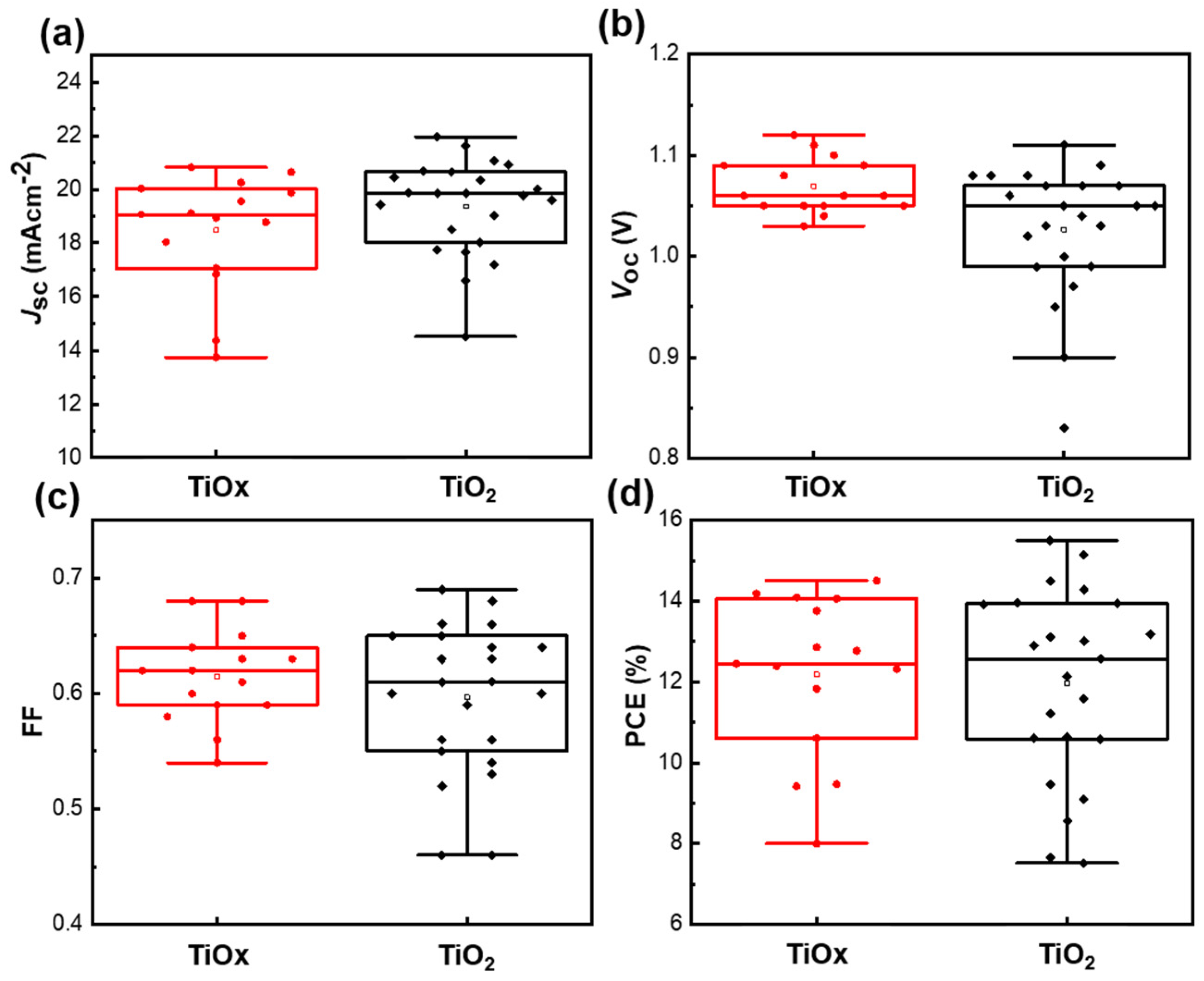
Figure 1. (a) Schematic illustration of the chemical bath deposited titanium dioxide (TiOx) films, as well as their corresponding thermal treatments at 150 °C for 1 h and 450 °C for 30 min; XPS spectra of TiOx and titanium oxide (TiO2), (b) O1s, and (c) Ti2p; (d) Raman spectra of TiOx and TiO2 films; and water contact angles of the (e) TiOx and (f) TiO2 films on an FTO substrate.
Nanomaterials 10 01676 g001
Figure 2. SEM images of the (a) TiOx film and (b) TiO2 film; atomic force microscopy (AFM) images of the (c) TiOx film and (d) TiO2 film; and cross-section SEM images of the (e) TiOx film and (f) TiO2 film.
Nanomaterials 10 01676 g002
Figure 3. Top-view SEM images of the (a) TiOx/MAPbI3 film and (b) TiO2/MAPbI3 film, and cross-sectional SEM images of the (c) FTO/TiOx/MAPbI3 film and (d) FTO/TiO2/MAPbI3 film.
Nanomaterials 10 01676 g003
Figure 4. (a) XRD pattern of the perovskites formed on the TiOx and TiO2 films, and (b) photoluminescence (PL) spectra of the perovskites formed on the FTO substrate, FTO/TiOx film, and FTO/TiO2 film.
Nanomaterials 10 01676 g004
Figure 5. Nyquist plots of perovskite solar cells (PSCs) based on (a) TiOx and (b) TiO2 in the dark at a DC bias of 0 V. A 1–V AC signal was applied with a frequency range of 20 Hz–1 MHz. The inset shows the equivalent circuit model of the resultant devices.
Nanomaterials 10 01676 g005
Figure 6. (a) Schematic of the complete device configuration, (b) reverse scan J–V curves of the TiOx- and TiO2-based PSCs, (c) incident photon-to-conversion efficiency (IPCE) spectra of the TiOx- and TiO2-based PSCs, and (d) histogram of the power conversation efficiencies (PCE) of PSCs with the TiOx and TiO2 films.
Nanomaterials 10 01676 g006
Figure 7. Average (a) Jsc, (b) Voc, (c) fill factor (FF), and (d) PCE values for devices fabricated with TiOx and TiO2 films. Error bars indicate ± one standard deviation from the mean.
Nanomaterials 10 01676 g007
Table 1. Summary of the parameters for the PSCs (FTO-glass/TiOx or TiO2/MAPbI3/Spiro-OMeTAD/Au). The statistical analysis (average ± standard deviation) was based on the measurements of 18 and 26 individual devices with TiOx and TiO2, respectively. Champion refers to the device with the highest PCE.
ETLs Layer JSC (mA/cm2)Voc (V)FFPCE (%)
TiOxChampion20.641.120.6314.51
Average ± SD18.3 ± 2.31.07 ± 0.030.61 ± 0.0412.1 ± 2.1
TiO2Champion21.061.080.6815.50
Average ± SD19.2 ± 1.91.02 ± 0.070.59 ± 0.0711.9 ± 2.4

