Article

CVD Synthesis of Intermediate State-Free, Large-Area and Continuous MoS2 via Single-Step Vapor-Phase Sulfurization of MoO2 Precursor

by
Tinna Chiawchan
1,
Harihara Ramamoorthy
2,*,
Kanokwan Buapan
1 and
Ratchanok Somphonsane
1,3
1
Department of Physics, Faculty of Science, King Mongkut’s Institute of Technology Ladkrabang, Bangkok 10520, Thailand
2
Department of Electronics Engineering, Faculty of Engineering, King Mongkut’s Institute of Technology Ladkrabang, Bangkok 10520, Thailand
3
Thailand Center of Excellence in Physics, Commission on Higher Education, 328 Si Ayutthaya Road, Bangkok 10400, Thailand
*
Author to whom correspondence should be addressed.
Nanomaterials 2021, 11(10), 2642; https://doi.org/10.3390/nano11102642
Submission received: 14 August 2021 / Revised: 29 September 2021 / Accepted: 1 October 2021 / Published: 8 October 2021

Abstract

:
The low evaporation temperature and carcinogen classification of commonly used molybdenum trioxide (MoO3) precursor render it unsuitable for the safe and practical synthesis of molybdenum disulfide (MoS2). Furthermore, as evidenced by several experimental findings, the associated reaction constitutes a multistep process prone to the formation of uncontrolled amounts of intermediate MoS2−yOy phase mixed with the MoS2 crystals. Here, molybdenum dioxide (MoO2), a chemically more stable and safer oxide than MoO3, was utilized to successfully grow cm-scale continuous films of monolayer MoS2. A high-resolution optical image stitching approach and Raman line mapping were used to confirm the composition and homogeneity of the material grown across the substrate. A detailed examination of the surface morphology of the continuous film revealed that, as the gas flow rate increased by an order of magnitude, the grain-boundary separation dramatically reduced, implying a transition from a kinetically to thermodynamically controlled growth. Importantly, the single-step vapor-phase sulfurization (VPS) reaction of MoO2 was shown to suppress intermediate state formations for a wide range of experimental parameters investigated and is completely absent, provided that the global S:Mo loading ratio is set higher than the stoichiometric ratio of 3:1 required by the VPS reaction.

1. Introduction

In the past few years, 2D-MoS2 has emerged as one of the most popular candidates among the 2D-TMDC family of materials. In contrast to graphene, 2D-MoS2 is a semiconductor with a non-zero bandgap, which allows for the realization of transistors with high on–off current ratios [1]. Moreover, the bandgap is tunable via modulation of the layer thickness, changing from an indirect-to-direct bandgap as the thickness approaches the monolayer limit [2,3]. The latter feature is especially beneficial for realizing optoelectronic applications, such as photodetectors and photo-emitters. As expected, the increased popularity of 2D-MoS2 has led to several demonstrations of FETs, photodetectors and sensors, as evident from the literature [4,5,6,7,8,9,10,11,12,13,14,15].
Furthermore, 2D-MoS2 can be synthesized by using either top-down approaches, such as chemical or mechanical exfoliation, or bottom-up synthesis routes, such as chemical vapor deposition (CVD). While mechanical exfoliation has been extensively used due to the resulting high sample quality, the obtained crystal sizes are random in nature, and the overall yield is often quite limited. This makes it difficult to extend their usability to practical applications. In comparison to exfoliation, CVD growth methods have showed great promise in terms of improved yield, scalability and homogeneity of the grown films, making it the method of choice for implementing future technology that could be made viable through integration with the current CMOS platform. However, to truly unlock the potential of 2D-MoS2 as a replacement material for conventional silicon, it is necessary to be able to produce large-scale, defect-free and continuous MoS2, using a low-cost and safe approach.
CVD-grown MoS2 has been synthesized via the sulfurization of Mo containing precursors, such as Mo [16], MoO2 [17,18,19,20] and MoO3 [21,22,23,24,25,26,27,28,29,30,31,32,33,34,35,36,37,38,39,40,41,42,43,44,45,46,47,48,49], among which the use of MoO3 powder as the precursor has remained the most popular method owing to the possibility of obtaining large area single crystal and also continuous films [41,42,43,44,45,46,47,48,49].In fact, in very recent work, Q. Wang et al. [46] have employed a customized multisource CVD system to successfully demonstrate the wafer-scale growth of MoS2 using MoO3 as the precursor material. While these accomplishments are noteworthy, the poisonous nature (strong irritant and carcinogen according to GHS classification) and low evaporation temperature (350 °C) of MoO3 powder means that harmful exposure to this material is more likely, posing a serious health hazard situation. A safer material choice is therefore needed for both small-scale research purposes and meeting large-scale production needs.
In a previous report, Bilgin et al. [17] raised an important question of whether the use of MoO3 as a precursor material is really necessary when MoO2, a more stable oxide, could be used instead. In their work, a direct vapor-phase sulfurization (VPS) of MoO2, which is characterized by a single-step chemical reaction MoO 2   +   3 S MoS 2   +   SO 2 , was employed to successfully grow MoS2 crystals. The crystals were shown to be not only possible to grow on a wide range of substrates such as Si, Si3N4, SiO2, quartz and mica, but were also of high optoelectronic grade, as assessed from the excitonic states observed from photocurrent spectroscopy measurements [17].
It is widely accepted that when MoO3 is used as the initial precursor, the final MoS2 product results from a two-step process: the first being the reduction of MoO3 to MoO2 (Equation (1)) which is then followed by a second step which involves the sulfurization of MoO2 (Equation (2)) [17,41].
MoO 3   +   x 2 S MoO 3 x   +   x 2 SO 2
MoO 3 x   +   7 x 2 S MoS 2   +   3 x 2 SO 2
As is evident from these equations, an ideal situation (x = 1) would result in the intermediate compound being MoO2. However, since growth conditions within a CVD furnace are rarely ideal, it was suggested that incomplete reactions could result in varying amounts of MoS2−yOy phase [17,50,51]. This “phase-mixing” with the MoS2 has been frequently observed in experiments [23,25,48,52] and remains an important issue that needs to be addressed.
Recently, through detailed experimental work varying the S:Mo molar ratio, the stepwise sulfurization of MoO3 to MoS2 via an intermediate reaction forming molybdenum oxysulfide (MoOS2) was reported [36]. The authors of this work have proposed the following reaction for the formation of MoOS2 from the intermediate phase MoO2.
2 MoO 2 ( v )   +   5 S ( v ) 2 MoOS 2 ( s )   +   SO 2 ( v )
The above reaction pathway suggests that, even in an ideal scenario (x = 1), where MoO3 is appropriately reduced to MoO2, the formation of intermediate states may not be fully avoidable.
The role of MoO2 as an intermediate phase was further investigated in a different study conducted by Hyun et al. [35]. Here, after the synthesis of MoS2, it was found that the MoO3 powder used for the growth was reduced by sulfur to form MoO2 powder. In addition, MoO2 crystals were also reported to be formed on the growth substrate. These findings were explained by proposing a thermodynamically favorable (negative Gibbs free energy change) reaction pathway (Equation 4) for the formation of solid-phase MoO2 from MoO3 powders [35].
4 MoO 3 ( s )   +   S 2 ( v ) 4 MoO 2 ( s )   +   2 SO 2 ( v )
Based on these observations, it was proposed that when using MoO3 powders as the precursor, a much more complex scenario could arise wherein the final MoS2 could potentially be synthesized by a number of thermodynamically favorable pathways. These include the sulfurization of vapor-phase MoO3, the sulfurization of intermediate solid-phase MoO2 state and finally the sulfurization of vapor-phase MoO2, resulting from the vaporization of the reduced MoO2 powder (see Equations (5)–(7)) [35].
4 MoO 3 ( v )   +   7 S 2 ( v ) 4 MoS 2 ( s )   +   6 SO 2 ( v )
4 MoO 2 ( s )   +   6 S 2 ( v ) 4 MoS 2 ( s )   +   4 SO 2 ( v )
4 MoO 2 ( v )   +   6 S 2 ( v ) 4 MoS 2 ( s )   +   4 SO 2 ( v )
Importantly, while all three proposed reactions are thermodynamically favorable with a negative Gibbs free energy change value, the reaction (Equation (7)) involving the direct VPS of MoO2 was found to have the most negative value for the Gibbs free energy change value, making it the most thermodynamically favorable reaction. This is followed by the VPS of MoO3 (Equation (5)), and finally the solid-phase sulfurization of MoO2 (Equation (6)) taking the highest Gibbs free energy change values [35].
It is clear from the thermodynamic considerations discussed thus far that a single-step VPS reaction of MoO2 should provide the best chemical pathway to synthesize MoS2 after taking into account the associated reaction simplicity, safety and ability to greatly suppress intermediate state formations if not fully eliminate it. Despite this, there have been only a few experimental studies dedicated towards evaluating the potential of directly using MoO2 as a precursor. Following the experimental works of Bilgin et al. [17], Xie et al. [18] studied the effect of growth parameters such as the S:Mo molar ratio and the introduction time of the sulfur for initiating MoS2 growth. These parameters were shown to affect the MoS2 domain shape which was found to be tunable from triangles to hexagons. While large area growth (centimeter scale) was reported, the MoS2 obtained were discreet single crystal domains and not continuous films. It was also suggested that the lower evaporation ability of MoO2 inhibits the coalescence of flakes and therefore also the probability of forming large-area continuous films.
In this work, we successfully grow centimeter-scale continuous films of monolayer MoS2 using the single-step VPS method prescribed by Bilgin et al. [17] We find that the final growth pattern takes the form of distinct parabolic growth zones containing varying morphology of the synthesized MoS2, which is typical of the presence of a concentration-gradient of the Mo-source across the growth substrate. Different from prior works, we employed a high-resolution optical image stitching approach to create a clear map of the growth zones, as well as to capture the area coverage of the continuous monolayer MoS2 typically found in the downstream zone. Detailed Raman point analyses, along with area and line scan mappings, are performed to confirm the material composition of the various zones and the homogeneity of the continuous films. The effect of varying gas flow rate in our experiments is carefully studied, and we find striking dependence of the morphology and quality of the grown films on this parameter, as determined using scanning electron microscopy (SEM). In particular, the increase of gas flow rate drives the CVD reaction from a thermodynamically stable regime to a kinetically unstable one and results in the drastic reduction in grain boundary separations of the continuous films. Additionally, by closely studying the effects of other growth parameters such as the MoO2 weight, S:Mo molar ratio and crystal growth time, we show that there are striking similarities in the growth results when compared to the results obtained from the conventional growth process employing MoO3 precursors.
The most significant finding of our work is that the synthesized MoS2 is found to be completely free of intermediate reaction by-products (such as MoO2 and MoOS2), as long as the S:Mo loading ratio is set above the stoichiometric value of 3:1 fundamentally required by the direct VPS reaction of MoO2 to properly form MoS2. For S:Mo ratios greater than 3:1, even the thickest material found on our growth substrate corresponds to fully sulfurized bulk MoS2 and not of any intermediate states, which strongly proves the overall effectiveness of using the single-step direct VPS of MoO2. This is in striking contrast to past reports employing MoO3 as the precursor, where intermediate states were a common observation, even as the S:Mo ratios were set at values orders of magnitude in excess of the stoichiometric requirements. We therefore believe that the results presented here should strengthen previous assertions of the logical choice of MoO2 as the precursor material and provide a platform for further exploration of the wafer-scale growth of continuous and homogenous MoS2 films, a prospective that holds tremendous promise for the future of semiconductor technology and CMOS scaling.

2. Materials and Methods

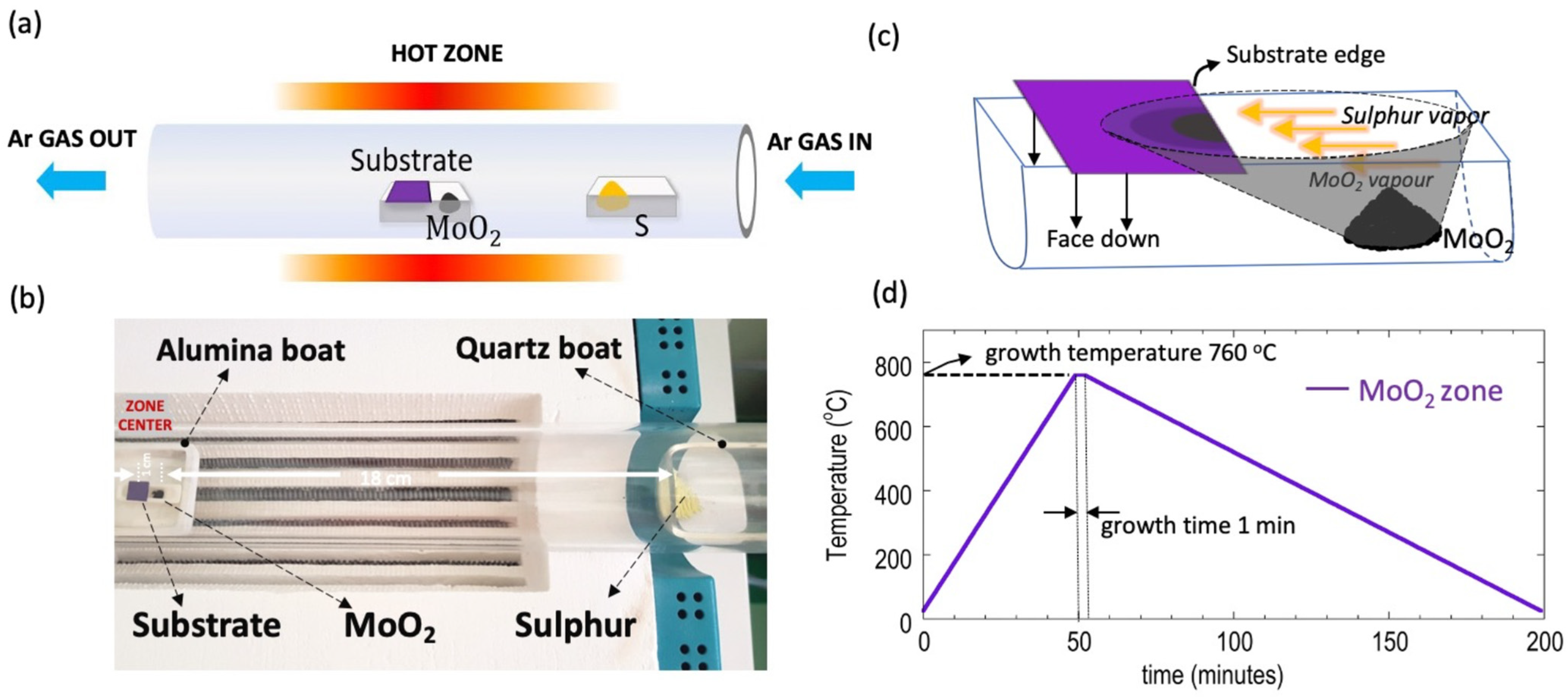
2.1. CVD Synthesis of MoS2 Using Direct MoO2 Precursor

Centimeter-scale continuous films of MoS2 reported in this work were synthesized using a simple atmospheric pressure CVD scheme similar to Bilgin et al. [17], with few changes. The CVD system consists of a single heating zone and a quartz tube of 50 mm diameter inside which the MoS2 growth takes place at a growth temperature of 760 °C. A 300 nm thermal oxide Si/SiO2 wafer is firstly cut into ~ 10 mm × 10 mm squares and subsequently cleaned with 1 min of ultrasonication in acetone, followed by an IPA rinse and finally blown dry with nitrogen gas. Without any further surface processing, the cleaned wafer is centered face-down on a small (26 mm × 8 mm × 7 mm) alumina boat preloaded with the required amount of MoO2 precursor (99% purity Alfa Aeser, Haverhill, MA, USA) placed at the upstream end of the boat, approximately 1 cm from the center of the growth substrate (see Figure 1a,b). The sample-and-precursor-containing boat is then placed on a second alumina boat, and the assembly is carefully inserted into the quartz tube, such that the substrate position aligns with the center of the heating zone. In a different quartz boat, the required amount of sulfur powder (99.5% Alfa Aeser, Haverhill, MA, USA) is loaded such that the sulfur is at the edge (approximately 18 cm from the center) of the heating zone (see Figure 1b). The tube is then purged with a 2000 sccm of Ar gas (>99.9% purity) for 5 min at room temperature. Following this, the flow rate is lowered to a value required by the experiment and the temperature of the heating zone is ramped up at the rate of 15 °C/min until the required growth temperature is reached and subsequently held here for the required growth time as designed by the experiment. At the end of the growth cycle, the power to the furnace is turned off and the sample is allowed to naturally cool down to room temperature. Figure 1d shows the typical growth zone temperature profile used in this work.

2.2. MoS2 Characterization

The quality and thicknesses of the grown MoS2 material was assessed by using optical imaging, micro-Raman spectroscopy, AFM and SEM analysis. Optical imaging and high-resolution image stitching were obtained by using a CX-40M microscope from Ningbo Sunny Instruments, Co., Ltd., Yuyao, China. The micro-Raman spectra were obtained from a Horiba LabRAM HR Evolution confocal Raman system (Horiba Ltd., Bangkok, Thailand) at a laser excitation wavelength of 532 nm. AFM was performed by using a AFM5500M system from Hitachi High-Tech Ltd., Bangkok, Thailand. A SU8030 Field-Emission Scanning Electron Microscope (FESEM) from Hitachi High-Tech Ltd., Bangkok, Thailand was used to analyze the surface morphology of the grown MoS2 films.

3. Results and Discussions

The quantity of active Mo species accessible at the substrate surface for nucleation and subsequent domain formation play a crucial role in the entire growth process of MoS2. While a uniform distribution of gaseous phase S is typically achieved by maintaining a large distance of separation between the S source and the growth substrate (~18 cm in our case), the Mo-containing source is typically placed in close proximity to the growth substrate. This results in a prominent gradient-like concentration distribution of the MoS2 nucleation sites at the substrate surface, which then serves as the blueprint for the final growth pattern (see schematic shown in Figure 1c). Numerical simulations performed by R. A. Vila et al. [53] using finite element modelling revealed a decreasing concentration gradient on the surface of the substrate as the distance from the Mo-source increases, and that the concentration gradient pattern is characterized as distinct parabolic growth zones commonly found in experiments [24,29,36,45,49]. Moreover, the presence of such a concentration gradient means that the local Mo:S ratio varies along the length of the growth substrate, increasing the probability of morphology evolutions [53], oxysulfide formations [33,36,48,50,51,52] and MoS2 domain-shape changes [24]. To make matters worse, experimental factors, such as precursor amount, gas flow rate, substrate position relative to the MoO3 source, growth temperature, geometrical parameters and possibly the spatial distribution of the MoO3 precursor itself, all have an impact on the Mo flux arriving at the substrate.

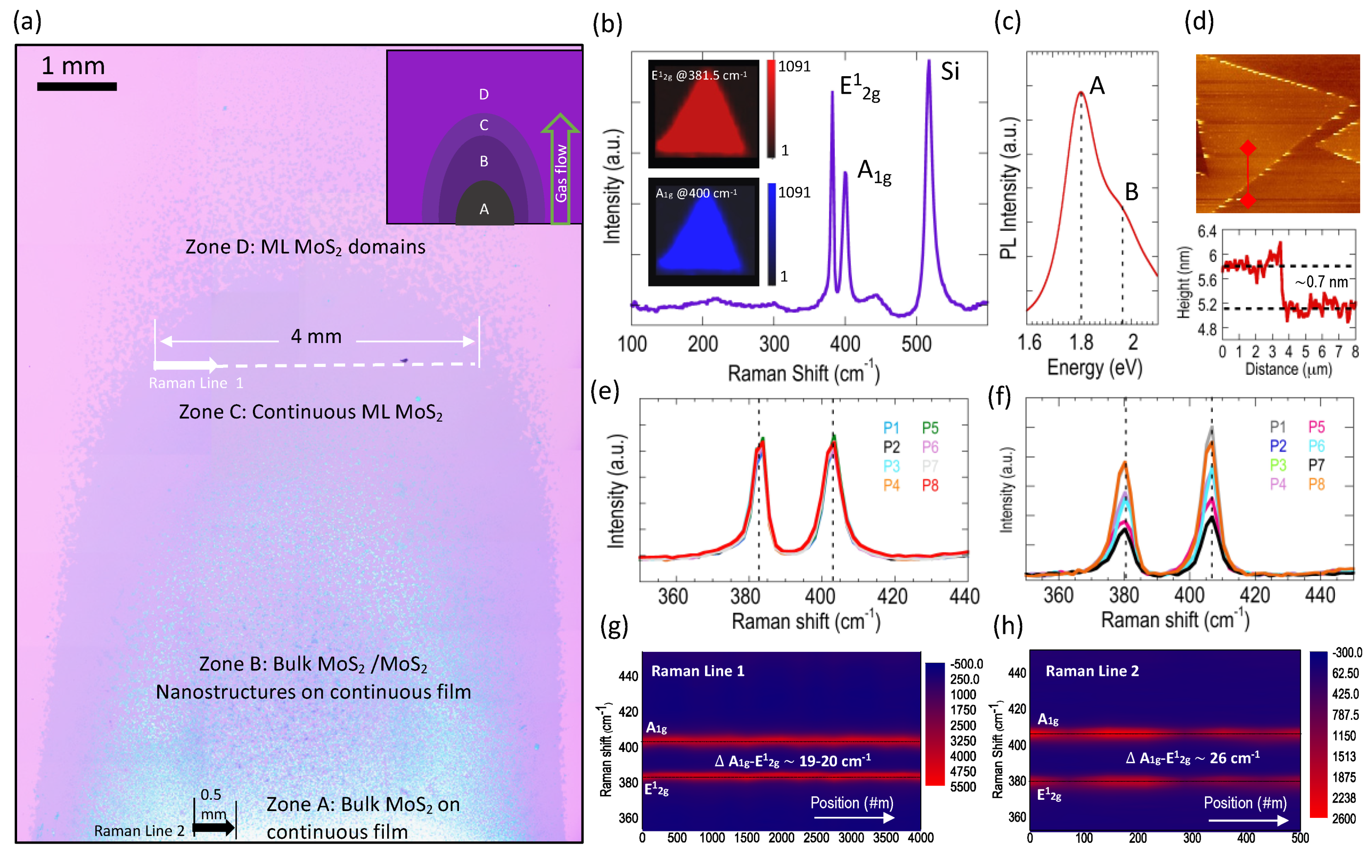
3.1. Zonal Deposition Pattern of MoS2

The aforementioned scenarios should also be expected when using MoO2, which is the precursor employed in our work. As a result, the formation of distinct growth zones can be expected, as shown in the schematic of Figure 1c, with each zone containing growth crystal with potentially varied characteristics. Experimentally, this can be directly seen in Figure 2a, where we show the MoS2 growth results obtained by using the following set of growth parameters: MoO2 amount = 3 mg, S amount = 300 mg, gas flow rate = 10 sccm, growth temperature = 760 °C and growth time = 1 min. The high S:Mo loading ratio of 100:1 is initially chosen to ensure complete sulfurization of MoO2 whereas the short growth time prevents the formation of nanoparticles on the MoS2 domains and thin films. The effects of these growth factors are investigated in detail, and they are discussed in the later sections.
Unlike previous reports, the high-resolution optical image stitching approach used in our work aids in the visualization of MoS2 film growth and its coverage across the entire growth substrate. As seen in Figure 2a, the image stitching reveals very clearly the formation of the four distinct, parabolic-shaped growth zones, A to D, marked by the dotted lines. Zone A which is closest to the substrate edge is dominated by a thick white-colored material. Zone B is seen to contain a mix of the white material (seen in Zone A) and “rod-like” nanostructures (discussed later). Zone C, as judged from the uniform optical contrast, represents a continuous layer of monolayer MoS2 and finally zone D is dominated by the formation of individual monolayer MoS2 domains.
Figure 2b shows the Raman spectra, obtained over a wide spectral range, for a MoS2 domain selected from a random location in zone D and in close proximity (~100 μm) to the boundary separating zones C and D. The two dominant Raman vibration modes which are characteristic of MoS2 can be seen here. The E12g mode, corresponding to the in-plane vibration of S and Mo atoms, is seen at a wavenumber of approximately 381.5 cm−1 and the A1g mode, corresponding to the out-of-plane vibrations of S atoms, is seen at about 400 cm−1. The resulting frequency difference ( Δ ω ) between the two modes is therefore ~18.5 cm−1, confirming the monolayer nature of the MoS2 domain [54,55]. In addition to the two Raman modes of MoS2, a third vibration peak corresponding to that of Si is observed at a wavenumber of 516 cm−1. The thickness uniformity of the MoS2 domain is further analyzed by using Raman mapping, the results of which are shown in the inset of Figure 2b. It is evident from the uniform Raman intensity maps, obtained at both vibration modes (E12g and A1g), that the thickness of the MoS2 domains grown in zone D is highly uniform. Figure 2c displays the photoluminescence (PL) spectra obtained for a monolayer MoS2 domain found in zone D. The characteristic A and B direct excitonic transitions that occur at ~1.81 and ~1.95 eV, respectively, and the relatively large A peak intensity, attest to the monolayer nature and the good crystalline quality of the grown MoS2 [2,17].
We additionally performed AFM imaging (Figure 2d), and the corresponding step height measurements revealed a thickness of ~0.7 nm. This value is in close agreement with the structural thickness of 0.615 nm for an isolated S-Mo-S slab, and therefore confirms the monolayer characteristics of the grown MoS2 triangles. To study the characteristics of the continuous MoS2 film grown in zone C, we performed an elaborate 25-point Raman line scan mapping (see Figure 2g) over a distance of 4 mm, marked by the white dotted line shown in Figure 2a. The film homogeneity is immediately apparent from the relatively unchanging E12g and A1g positions across the mapped line. The line scans revealed a frequency difference lying in the 19–20 cm−1 range, which confirms the monolayer nature of the continuous film. Corresponding Raman spectra is shown in Figure 2e for eight randomly picked points along the direction of the line scan. The full-width at half-maximum (FWHM) as calculated from these traces are ~4.5 and ~6 cm−1 for the E12g and A1g peaks, respectively, indicating good crystalline quality of the grown MoS2.
A second Raman line scan was performed to determine the composition of the thick white material grown in zone A. Figure 2f,h shows the line mapping results obtained over a 0.5 mm distance, marked by the black arrow in Figure 2a. In contrast to the results of Figure 2g, the frequency difference between the E12g and A1g peaks measured in this region is found to have a significantly higher value of ~26 cm−1, and therefore corresponds to bulk MoS2. As we additionally prove in the following discussions, using spectra collected over a wider wavenumber range, the thick material found in this region represents fully sulfurized bulk MoS2 and does not contain any intermediate by-products such as MoOS2. It must be noted that, in contrast to the overlapping Raman traces seen in Figure 2e, in Figure 2f there instead appears to be a random spread in the intensities across the mapped line (see color contour shown in Figure 2h). We believe these intensity variations are directly related to the thickness variations of the bulk MoS2 across the scanned locations. Similar intensity variations have been observed previously and were attributed to optical interference effects arising from the presence of the underlying oxide layer [55].
The formation of thick MoS2 material grown in zone A can be attributed to the high concentration of Mo-flux arriving at the leading edge of the substrate. As nucleation progresses further away from the sample edge, the nucleation density lowers and becomes favorable for the growth of triangular domains and their subsequent coalescence [23]. This ultimately results in zone C being covered with a continuous MoS2 film.

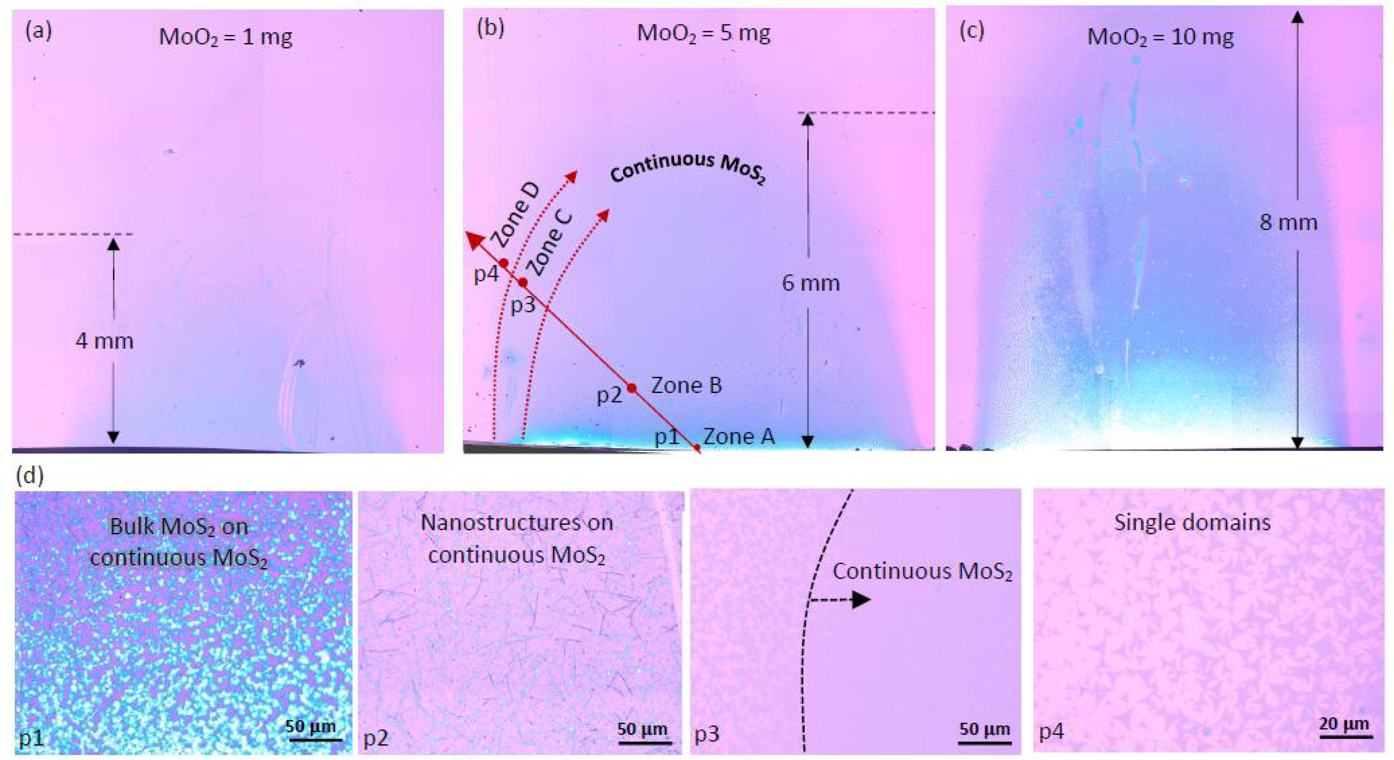
3.2. Effect of MoO2 Precursor Quantity

To demonstrate the significance of the Mo-flux, we performed an experiment in which the MoO2 quantity was varied while the gas flow rate was held constant at a high value of 100 sccm (Figure 3). The diffusion of MoO2 vapor from the source to substrate can be quantified by using a common solution to the diffusion equation [56]:
n ( x , t )   =   n ( 0 , t )   e x p [ x 2 4 D t ]
where t is the time, D is the diffusion constant and n ( 0 , t ) and n ( x , t ) are the concentrations of the gaseous species at the source and a distance x away from the source, respectively. Evidence of the n ( 0 , t ) dependency can be seen experimentally from the growth results shown in Figure 3a–c. Here, a systematic expansion of the growth zones is observed as the amount of MoO2 precursor is increased from 1 mg to 5 mg and 10 mg. For the case when 10 mg of MoO2 is used, the outermost growth zone extends all the way across the substrate length. Although this increase in wafer coverage may be viewed as beneficial, the simultaneous strengthening of the concentration gradient is undesirable as it results in more regions of the wafer being covered with thick MoS2 product, as clearly visible from the bright contrasted regions towards the upstream end of the substrate (Figure 3c). On the contrary, while the gradient produced by the smallest MoO2 quantity (1 mg) is not immediately apparent, the wafer coverage is evidently poor.
Figure 3d shows zoomed-in images captured at the locations p1 through p4, marked in Figure 3b. Each image captures the growth morphology in the respective zones A to D (also marked in Figure 3b). An accidental scratch mark at location p2 revealed that the nanostructures discovered at this location were actually formed on top of a continuous bottom layer. This was later found to be true for the bulk MoS2 crystals grown in zone A, as well.

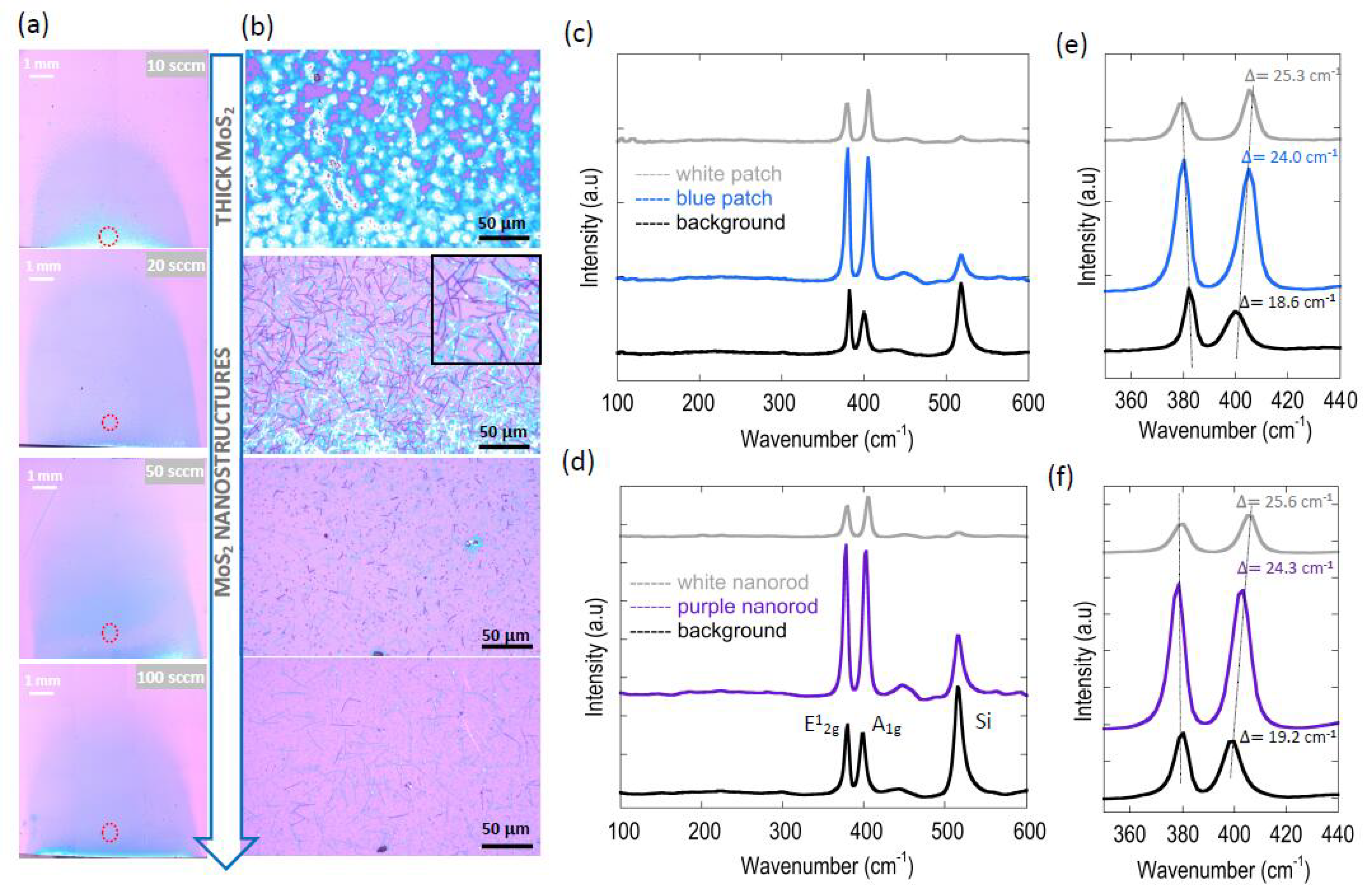
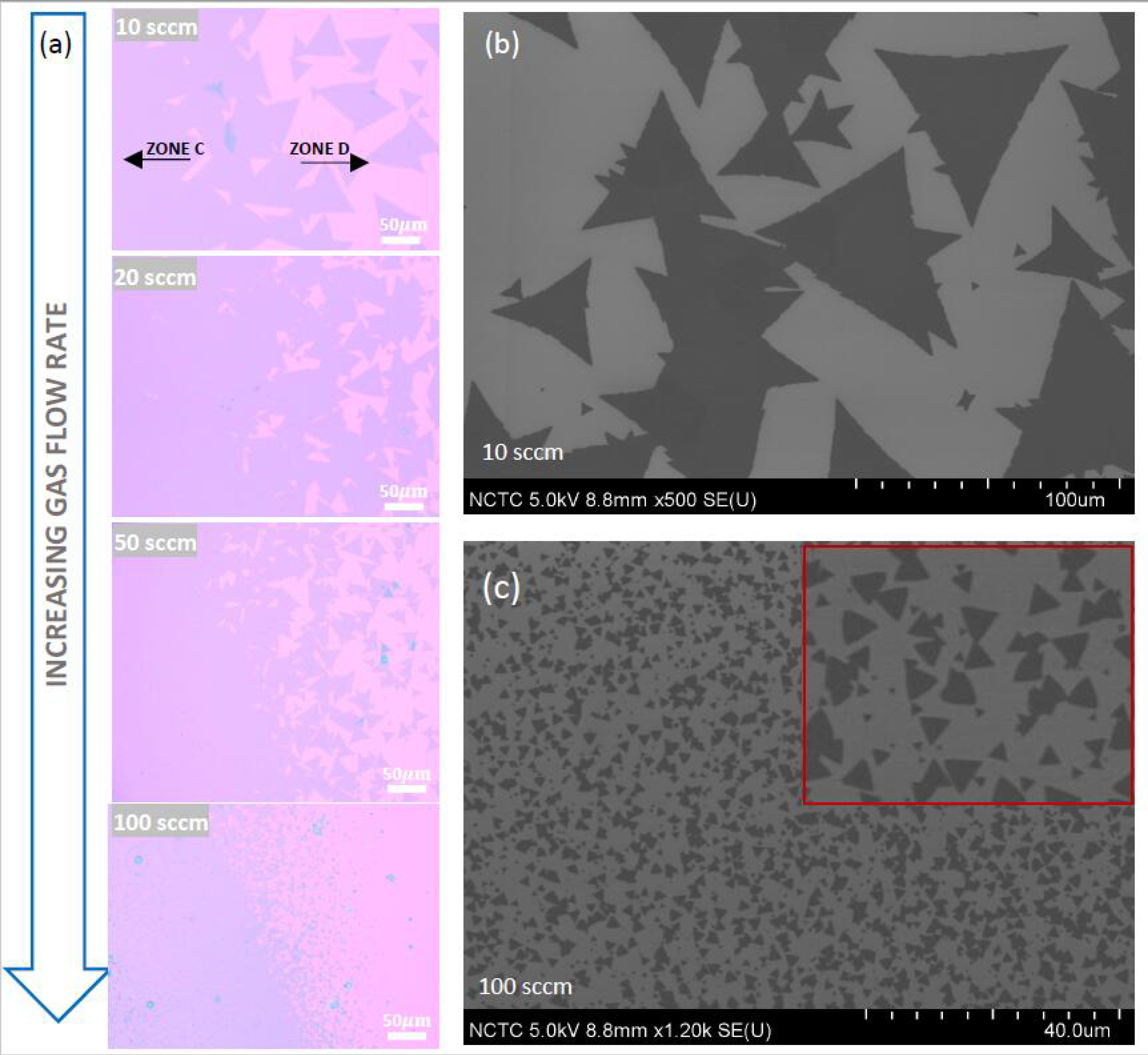
3.3. Effect of Gas-Flow Rate on MoS2 Morphology

To further explore the aforementioned phenomenon, we performed a detailed investigation of the effect of gas-flow rate on growth conditions, the results of which are presented in Figure 4, Figure 5 and Figure 6. The immediate observation from the stitched optical images shown in Figure 4a is that close to the leading edge of the growth substrate (marked in Figure 4a) the concentration gradient is seen to be significantly dampened as the flow rate is increased. Interestingly, the growth of nanostructures was observed for growth using higher gas flow rates, as evident from the optical images corresponding to the gas flow rate conditions of 20, 50 and 100 sccm (see Figure 4b). For the lowest flow-rate condition of 10 sccm, these nanostructures are largely absent, and the growth was dominated by thick MoS2 material.
Similar nanostructures have been reported in prior works [29,53,57,58], using an MoO3 precursor. According to Vila et al. [53], depending on the MoOx:S2 partial pressure available at the growth site, these nanostructures can be fully MoO2, partially sulfurized MoO2 or even MoS2. Therefore, to verify the structural composition of the thick material and the nanostructures, we performed Raman analyses for each of these cases. As can be seen from the data shown in Figure 4c,d, the Raman scan obtained in a wide wavenumber range of 100–600 cm−1 revealed only two peaks (A1g and E12g), which are characteristic of MoS2 material, in addition to the expected peak of Si seen at a wavenumber of 516 cm−1. There were no peaks corresponding to MoO2 or MoOS2 at any of the six locations analyzed, indicating that complete sulfurization of MoO2 occurred. Interestingly, the Raman traces obtained from the background revealed that these regions were covered with a continuous film of monolayer MoS2 (peak differences of 18.6 and 19.2 cm−1 for 10 and 20 sccm cases, respectively), indicating that the thicker material and nanostructures could have grown after the formation of an initial layer of monolayer MoS2. Such a “layer-plus-island” growth mode may indicate that the surface and edge energy ( Δ E ) changes from initially being negative ( Δ E   <   0 ) to taking positive values ( Δ E     0 ) later [53,59].
Figure 4e,f show the corresponding spectrum of Figure 4c,d, respectively, but for a narrower spectral range. Here the thickness difference between the detected locations is evident. For example, while the background film exhibited a peak difference of 18.6 cm−1, confirming its monolayer nature, the blue- and white-colored patches exhibited peak difference values of 24 and 25.3 cm−1 respectively, and therefore corresponds to significantly thicker/bulk MoS2 material. Similar observations are also made for the nanostructures that were grown at the gas flow rate condition of 20 sccm (see Figure 4f).
Surprisingly, as seen in the various panels of Figure 4a, the bright patches at the leading edge of the substrate do not systematically dampen as the flow rate increases. For example, while we observe no regions of bulk MoS2 formation at the flow rate of 20 sccm, these regions seem to reappear at higher flow rates of 50 and 100 sccm. This rather unexpected result can be explained in terms of the substrate edge driving changes in the nucleation process [23]. Because the substrates were individually cleaved prior to growth, it is conceivable that the morphology of the edges could differ dramatically from one substrate to the next, resulting in this undesirable yet unavoidable effect on the ultimate growth result.

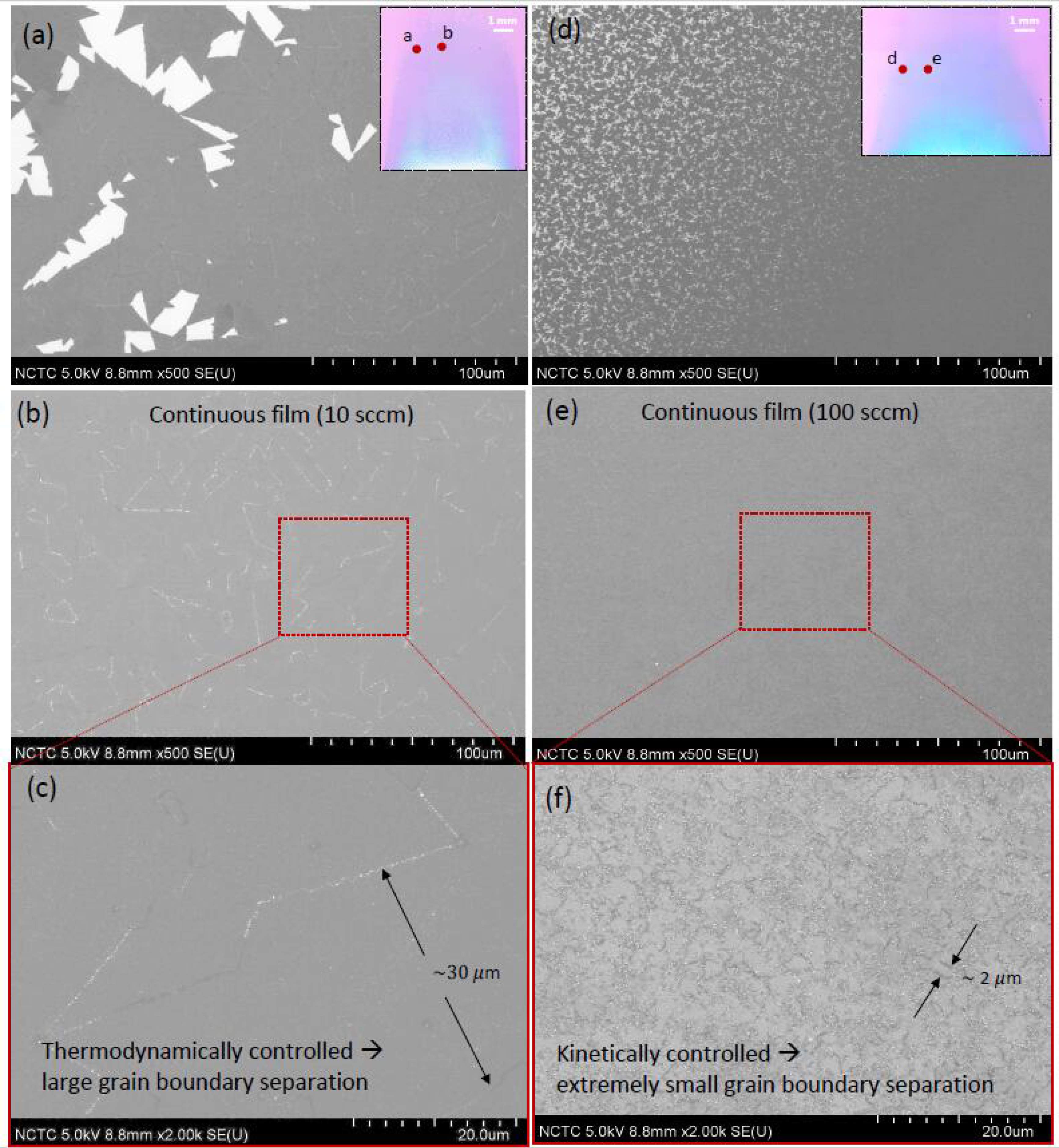
3.4. Effect of Gas-Flow Rate on Domain Size and Grain-Boundary Separation of Continuous MoS2

In addition to creating favorable growth conditions for the formation of nanostructures, the flowrate also plays a significant role in determining the average size of the individual MoS2 domains grown in zone D. As discussed in the following sections, this is a very important parameter that determines the quality of continuous films found in zone C. As the flow rate is increased from 10 to 100 sccm, the average domain size is reduced dramatically, from ~70 μm to less than 2 μm (see Figure 5a). The FESEM scans comparing the 10 and 100 sccm case are shown in Figure 5b,c, respectively. These results are in agreement with previous studies on the growth of graphene domains [60], where it was noted that a lower flow rate suppresses the nuclei density, which then facilitates the growth of larger domains. Z Lin et al. [26] reported a similar effect on nuclei density dependent domain sizes for MoS2 grown by using MoO3 precursor; however, the change in nuclei density reported in their work was due to the change in relative position of the substrate to the precursor source.
Given the dramatic effect on the domain size on the gas flow rate, it is imperative to investigate the surface morphologies of the continuous films. Figure 6 shows a comparison of FESEM images of the MoS2 layers grown at a flow rate of 10 sccm (Figure 6a–c) and 100 sccm (Figure 6d–f). Figure 6a,d captures the images at the boundary separating the continuous films and the individual domains (see insets identifying the location scanned). The magnitude of the difference in domain sizes between low and high flow rates is striking, as can be seen here. Figure 6b,e captures similar magnification images of those shown in Figure 6a,d, but for an area containing only the continuous film. For the 10 sccm flow rate condition, the grain boundaries are immediately visible and a zoomed in image (Figure 6c) reveals that, on an average, the grain boundary separations range between 20 and 30 μm, with certain regions even exceeding these values. The thickness uniformity over several tens of micrometers is made possible by the growth of large domain sizes, which indicates the high quality of the grown films [23,61]. On the other hand, the high-flow-rate condition of 100 sccm severely affects sample quality. While a lower magnification SEM image (panel (e) of Figure 6) reveals what may appear to be a continuous film without any grain boundaries, careful inspection at a higher magnification (panel (f) of Figure 6) proves, without doubt, the existence of extremely small grain (~2 μm) boundary separations in the grown film.
These results signify that an increased flow rate speeds up the mass transfer process, resulting in a faster crystal growth rate [24]. The latter introduces a high level of instability in the growth process by disallowing atoms to move into (and grow freely) at locations with the lowest surface free energy, leading to a so called “kinetically controlled” growth condition in contrast to a thermodynamically controlled one that is favored under low flow rate conditions.
In addition to the flow rate’s effect on the concentration gradient and the domain sizes, it is also noted from Figure 4a that substrate coverage can be improved with a higher flow rate (compare 10 and 20 sccm); however, a limit is apparently reached as we approach the highest flow rate of 100 sccm explored here. A tradeoff therefore exists between achieving better wafer coverage versus obtaining continuous films containing larger domain sizes. A strategy to improve wafer coverage is described in the later sections.

3.5. Influence of Critical Growth Parameters on MoS2 Domain Shape and Size

It should be clear by now that a thorough understanding of how domain attributes might be adjusted to achieve desirable qualities in the continuous films is required. We have therefore performed additional tests to explore the impacts of MoO2 amount, S amount and growth duration (Figure 7).

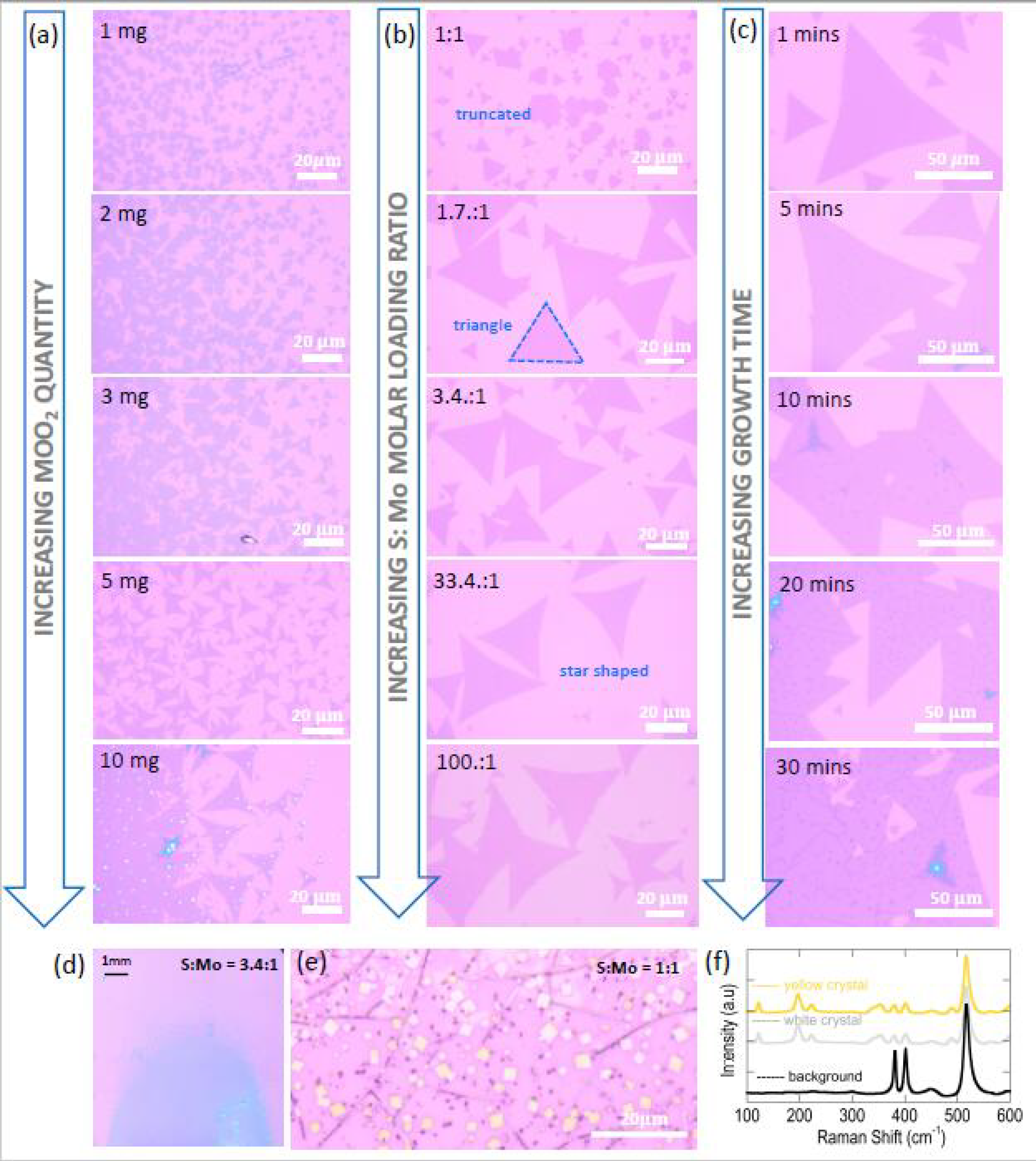
3.5.1. Domain-Size Dependency on MoO2 Precursor Amount

In addition to tuning domain size by using flow rate, the quantity of MoO2 precursor used also plays an important role. This can be seen in Figure 7a, which reveals a systematic increase in domain size as the precursor amount is increased. For a MoO2 quantity of 10 mg, the largest domain sizes are obtained. However, it must be recalled from the results of Figure 3c that a MoO2 quantity increase is also associated with a much stronger concentration gradient across the length of the sample. Unfortunately, this means that the domains formed are not homogenous and could potentially contain regions of thick MoS2, as is rightly revealed by the optical image taken for the 10 mg case (Figure 7a). In this regard, there is a trade-off in that the amount of MoO2 precursor used must be carefully chosen in order to achieve the required gradient distribution and domain sizes.

3.5.2. Domain Shape Dependency on S:Mo Molar Loading Ratio and Identifying the Regime of Intermediate-State-Free Growth of MoS2

Turning our attention to domain shape, we can observe from the growth results already shown in Figure 5a that the formed MoS2 domains are closer to a star shape rather than triangular. This is a well-known consequence of the presence of a S-rich growth condition [24,31], which, in our case, was created by the high value of S:Mo molar loading ratio of 100:1 set for the experiment. However, if desired, the domain shape can be tuned by lowering the S:Mo ratio until the stoichiometric requirement is reached to form perfect triangular domains. This is evident from Figure 7b, where a systematic evolution from a star shape to triangular domain is observed as molar loading ratio S:Mo is lowered in steps from 100:1 to 1.7:1. When the loading ratio is further reduced to 1:1, there are two significant deviations in the growth result. First, we see much smaller triangular domains along with truncated triangles in the mix. The formation of truncated domains is consistent with what is expected for a S-deficient condition and has been reported previously by other groups [23,24,31,34] that have used traditional MoO3 as the precursor. Second, and perhaps most intriguingly, we discovered how this S-deficient condition resulted in the formation of intermediates near the substrate’s leading edge (Figure 7e). While this effect was most pronounced for a loading ratio of 1:1, trace amounts with much smaller crystal sizes were also seen at a loading ratio of 1.7:1. Raman spectra shown in Figure 7f confirmed these crystals to be MoOS2. The point analysis that was performed on the background film revealed that it was monolayer MoS2 with a peak difference of ~20 cm−1. These findings imply that there may be competing mechanisms of growth involving formations of both MoS2 and MoOS2, especially when the growth conditions become S-deficient.
It is worth noting that, with the exception of the lowest S:Mo molar loading ratios of 1:1 and 1.7:1 (intermediates almost unnoticeable at this value), no intermediate state formations were observed from careful optical inspection of the MoS2 material grown from all other S:Mo conditions. As matter of fact, both MoO2 and MoOS2 are known to have very distinct morphologies (rectangular domains) when compared to MoS2, and they can therefore be easily identified on a substrate, using simple optical microscopy. The rather interesting revelation from our findings is in contrast to findings of previous experiments employing MoO3 as the precursor. To provide further validation, a few examples can be taken from the literature. For instance, Pondick et al. [36] reported that trace amounts of intermediate MoOS2 states were formed at the leading edge of the substrate, even with a globally set molar loading ratio as large as 187:1. Najmaei et al. [23] reported that a sulfur concentration greater than 500 mg was needed to avoid oxysulfide formations. Similarly, in Reference [25], a molar ratio greater than 170:3 was required to avoid intermediate products.
For MoOS2 to fully form from the reaction dictated by Equation (3) [36], the S:Mo ratio available for reaction must be 2.5:1. Likewise, to completely form MoS2 from the direct VPS of MoO2, the stoichiometric requirement is 3:1 (see Equation (7)). Therefore, to be sure that the intermediate reactions can be bypassed, a minimum S:Mo loading ratio of 3:1 should be used for reliable growth of intermediate-free MoS2, which is consistent with our experimental findings (an example of the growth pattern obtained at a molar ratio of 3.4:1 is shown in Figure 7d). Furthermore, because the outcome of the growth can be explained directly in terms of the global loading ratio set by the experiment, this could indicate a much closer agreement between the globally set S:Mo ratio and the locally available S:Mo ratio for reaction at the substrate. In this context, the single step VPS of MoO2 may provide a more effective means to control CVD growth parameters when compared with the traditional route of growing MoS2, using the VPS of MoO3.
Having highlighted these significant differences, it should be noted that a direct comparison of the molar ratio dependence reported in this work with those obtained by others should be approached with caution, because experimental conditions of the CVD setup can vary greatly. Importantly, because the local S:Mo ratio is the ultimate factor deciding the outcome of the growth material, geometrical factors must also be considered. For example, while the distance between the S and the growth substrate set in Reference [36] is close to the value used in our study, the CVD tube size was significantly different (1-inch o.d. in Reference [36] compared to 2-inch o.d. in our study).

3.5.3. Influence of CVD Growth Time on Nanoparticle Formations

In Figure 7c we show the effect on the domains when increasing the growth time from 1 min to a maximum of 30 min. The key consequence observed here is an acceleration of the creation of self-seeding nucleation sites (nanoparticles) on top of the MoS2 domains, as growth time increases. The nanoparticles start to appear as early as 5 min and systematically increase in density as the growth time is increased. Similar nucleation sites formed on top of MoS2 domains have been reported previously [37,62]. In Reference [37], the self-seeding mechanism was reported to be caused by increasing growth temperature, while in Reference [62], the increase of growth time has been shown to cause the same effect. We found that when the growth time is limited to 1 min, these nanoparticles are typically not present. This allowed us to grow materials that are more homogenous (see Figure 2a and Figure 5a) and have a reduced risk of additional layer formations stemming from these seeds. In prior work by Bilgin et al. [17] the rapid formation of second layers was reported, albeit at a much higher growth temperature of 950 °C. In addition to the inherent acceleration provided by the absence of intermediate state formations in the direct VPS of MoO2, this finding was attributed to the faster growth kinetics resulting from the higher temperature used for the growth. While the MoS2 domains reported in our work commonly revealed domain edge irregularities (expected for S-rich conditions), we do not observe any significant secondary layer formation when the domains are viewed under optical contrast, SEM imaging or AFM measurements. We attribute this to both the lower temperature (760 °C) and the short growth time employed in our work. This is in agreement with earlier findings [17] and emphasizes the important role of the growth temperature. While we did not conduct a comprehensive study of the effect of growth temperature in this work, we found that lowering the temperature below 700 °C resulted in a low MoS2 yield with no continuous monolayer formation. For growth temperatures greater than 800 °C, however, we found that the grown material was thick and non-homogeneous throughout the growth zones. Monolayer MoS2 (typically found in zones C and D) was consistently obtained when the growth temperature was set to an intermediate temperature of ~760 °C, which led us to select this temperature as the optimal growth temperature in the current study. While these findings indicate a strong temperature dependence of nucleation density, more detailed experiments (not performed here) examining changes in film growth with systematically varying the growth temperature will be required to fully comprehend the intricate growth mechanisms involved.

3.6. Effect of Precursor Spatial Distribution on Wafer Coverage

While we believe that the results presented in this work are a significant step forward, we have not yet demonstrated wafer-scale growth and/or wafer-scale uniformity of continuous monolayer MoS2. In a recent work employing MoO3 precursors [49], two kinds of growth regimes were identified: a diffusion regime and a surface-reaction regime, which corresponded to whether a large or small amount of MoO3 precursor was used for the growth, respectively. While in the diffusion regime, a gradient-like growth pattern, similar to those found in this work, was observed, in the surface reaction regime, the growth of continuous films with more than 90% wafer coverage was reported. The authors have attributed this to the reduction of the gas-phase reaction facilitated by the low MoO3 precursor quantity used and the low-pressure CVD growth conditions. In our experiments, we do not seem to transition into the surface-reaction mode, despite performing experiments with a very low (1 mg) MoO2 quantity (see Figure 3a). The reasons for this are not fully clear; however, in addition to the obviously different CVD process used (APCVD vs LPCVD), other geometrical factors, such as the source to substrate gap height/distance, could also play a significant role in limiting growth to the diffusion regime.
While further studies are warranted, a few other strategies to improve wafer coverage can also be considered. For instance, wafer-scale growth was very recently reported by Q Wang et al. [47] Here a specially designed multisource tube furnace was employed which allowed for a uniform distribution of Mo precursors to arrive at the growth substrate for nucleation. Other approaches, including the strategic introduction of S [45], increasing the substrate-source gap height [26], orienting the substrates vertically [28], and using barriers [48] have resulted in continuous films. In a much earlier work by Najmei et al. [23], the strategic placement of step edges across the growth substrate was also shown to promote uniform nucleation over a large area.
Here, we present a different approach that provided a modest improvement in wafer coverage. In an attempt to create a uniform distribution of Mo species with minimal to no gradient, we spread the MoO2 precursor uniformly across the entire length of the boat. Figure 8a shows the growth results obtained for such a scenario, while keeping all other growth parameters unchanged. A distinct pattern of film growth can be seen here, completely different from the zonal patterns observed for all other cases when the precursor was simply placed as a heap at a determined location on the boat. Interestingly, from Figure 8a it is evident that the growth of these films tends to initiate from all four edges of the substrate and then progress towards the center of the wafer, although not quite reaching there. This observation once again proves the strong influence that substrate edges and defects could possibly have in determining the final outcome of the growth processes, strongly in agreement with earlier findings by Najmei et al. [23]. We also found that, by increasing the flow rate, we could achieve improved wafer coverage (see Figure 8b,c), albeit with poor film thickness and morphology uniformity. For instance, a flow rate of 100 sccm yielded an entire substrate covered with growth material. However, as already noted, the higher flow rate drives the reaction towards unstable conditions and results in the formations of undesirable nanostructures on top of the MoS2 film. Additionally, we found it very difficult to achieve a uniform spread of the MoO2 across the boat, mainly due the small amounts of MoO2 used, and the fact that this step was being performed manually. Due to these reasons, no solid conclusions can be made at this point about the efficacy of this strategy, but we believe the insights derived from this paper may be beneficial for future works.

4. Conclusions

In conclusion, we have successfully demonstrated the possibility of growing continuous films of monolayer MoS2, using the single-step VPS of MoO2. The growth results exhibited a predominant zonal pattern which is typical of the presence of a varying concentration-gradient of the Mo-source impinging on the substrate surface. By employing a high-resolution optical-image-stitching approach, we could identify four distinct growth zones. At the upstream end of the substrate, growth was dominated by thick materials and “rod-like” nanostructures grown on top of continuous MoS2, while a cm-scale continuous film of monolayer MoS2 was grown in the downstream location. This was followed by the growth of individual MoS2 domains at the outermost growth zone.
The continuous MoS2 films grown in this work had a large area and were homogenous, as confirmed by Raman line map analysis. More importantly, the grain size of domains coalescing into continuous layers was found to be a strong function of the gas-flow rate used in the experiment. An order of magnitude reduction from ~30 to ~2 μm in grain-boundary separations was observed from SEM micrographs, as the gas flow rate was increased from 10 to 100 sccm, respectively, which meant that higher-quality MoS2 films were grown at the lowest gas-flow-rate condition. The dramatic effect of the gas-flow rate suggests that, as the gas-flow rate is increased, the growth process transitions from a thermodynamically controlled and stable process to a kinetically controlled and unstable one.
A significant finding of this work is that, for a wide range of S:Mo loading ratios investigated, the material synthesized on all identified growth zones was found to be solely MoS2, as confirmed by extensive Raman analyses, with no additional Raman peaks corresponding to any intermediate states, such as MoOS2 or MoO2. This is in striking contrast to previous reports using MoO3 as the precursor, where the formation of intermediate MoOS2 states was found to be a significant outcome of the growth process, even at excessively high S:Mo molar loading ratios. This further confirms earlier assertions of the efficacy of using a single-step VPS method for synthesizing MoS2. Our experiments reveal that the formation of intermediate states are highly disfavored, as long as the global S:Mo molar ratios are kept above the value of 3:1, which is stoichiometrically required by the VPS reaction of MoO2.
Finally, while we have yet to demonstrate wafer-scale continuous MoS2 growth by using the direct VPS of MoO2, a strategy to improve coverage via uniform distribution of the MoO2 source was tested and appeared to yield promising results. However, more work is needed to improve the homogeneity of the grown films. We believe that the simple reaction mechanics of the VPS of MoO2 and the associated high level of safety of using this material as the precursor make this a promising avenue for realizing wafer-scale monolayer MoS2 that is not only of high quality but also compatible with existing CMOS standards.

Author Contributions

Conceptualization, H.R.; methodology, T.C. and K.B.; validation, T.C., H.R. and R.S.; formal analysis, H.R.; investigation, T.C.; resources, T.C. and K.B.; data curation, T.C. and H.R.; writing—original draft preparation, H.R.; writing—review and editing, T.C., H.R., K.B. and R.S.; visualization, H.R., R.S. and T.C.; supervision, R.S.; project administration, R.S.; funding acquisition, H.R. and R.S. All authors have read and agreed to the published version of the manuscript.

Funding

This work was financially supported by Office of the Permanent Secretary, Ministry of Higher Education, Science, Research and Innovation (Grant No. RGNS-63-249). This work by King Mongkut’s Institute of Technology Ladkrabang has also received funding support from the NSRF (Grant No. RE-KRIS/031/64).

Data Availability Statement

The data presented in this study are openly available in FigShare at https://doi.org/10.6084/m9.figshare.15168456.

Conflicts of Interest

The authors declare no conflict of interest. The funders had no role in the design of the study; in the collection, analyses or interpretation of data; in the writing of the manuscript; or in the decision to publish the results.

References

  1. Radisavljevic, B.; Radenovic, A.; Brivio, J.; Giacometti, V.; Kis, A. Single-layer MoS2 transistors. Nat. Nanotechnol. 2011, 6, 147–150. [Google Scholar] [CrossRef] [PubMed]
  2. Splendiani, A.; Sun, L.; Zhang, Y.; Li, T.; Kim, J.; Chim, C.Y.; Galli, G.; Wang, F. Emerging photoluminescence in monolayer MoS2. Nano Lett. 2010, 10, 1271–1275. [Google Scholar] [CrossRef] [PubMed]
  3. Mak, K.F.; Lee, C.; Hone, J.; Shan, J.; Heinz, T.F. Atomically thin MoS2: A new direct-gap semiconductor. Phys. Rev. Lett. 2010, 105, 2–5. [Google Scholar] [CrossRef] [PubMed] [Green Version]
  4. Yin, Z.; Li, H.; Li, H.; Jiang, L.; Shi, Y.; Sun, Y.; Lu, G.; Zhang, Q.; Chen, X.; Zhang, H. Single-layer MoS2 phototransistors. ACS Nano 2012, 6, 74–80. [Google Scholar] [CrossRef] [Green Version]
  5. Late, D.J.; Huang, Y.K.; Liu, B.; Acharya, J.; Shirodkar, S.N.; Luo, J.; Yan, A.; Charles, D.; Waghmare, U.V.; Dravid, V.P.; et al. Sensing behavior of atomically thin-layered MoS2 transistors. ACS Nano 2013, 7, 4879–4891. [Google Scholar] [CrossRef]
  6. Lopez-Sanchez, O.; Lembke, D.; Kayci, M.; Radenovic, A.; Kis, A. Ultrasensitive photodetectors based on monolayer MoS2. Nat. Nanotechnol. 2013, 8, 497–501. [Google Scholar] [CrossRef]
  7. Mak, K.F.; He, K.; Lee, C.; Lee, G.H.; Hone, J.; Heinz, T.F.; Shan, J. Tightly bound trions in monolayer MoS2. Nat. Mater. 2013, 12, 207–211. [Google Scholar] [CrossRef]
  8. Perkins, F.K.; Friedman, A.L.; Cobas, E.; Campbell, P.M.; Jernigan, G.G.; Jonker, B.T. Chemical vapor sensing with monolayer MoS2. Nano Lett. 2013, 13, 668–673. [Google Scholar] [CrossRef]
  9. Salehzadeh, O.; Tran, N.H.; Liu, X.; Shih, I.; Mi, Z. Exciton kinetics, quantum efficiency, and efficiency droop of monolayer MoS2 light-emitting devices. Nano Lett. 2014, 14, 4125. [Google Scholar] [CrossRef]
  10. Wu, W.; Wang, L.; Li, Y.; Zhang, F.; Lin, L.; Niu, S.; Chenet, D.; Zhang, X.; Hao, Y.; Heinz, T.F.; et al. Piezoelectricity of single-atomic-layer MoS2 for energy conversion and piezotronics. Nature 2014, 514, 470–474. [Google Scholar] [CrossRef]
  11. Xue, F.; Chen, L.; Wang, L.; Pang, Y.; Chen, J.; Zhang, C.; Wang, Z.L. MoS2 tribotronic transistor for smart tactile switch. Adv. Funct. Mater. 2016, 26, 2104–2109. [Google Scholar] [CrossRef]
  12. He, G.; Ghosh, K.; Singisetti, U.; Ramamoorthy, H.; Somphonsane, R.; Bohra, G.; Matsunaga, M.; Higuchi, A.; Aoki, N.; Najmaei, S.; et al. Conduction mechanisms in CVD-Grown monolayer MoS2 transistors: From variable-range hopping to velocity saturation. Nano Lett. 2015, 15, 5052–5058. [Google Scholar] [CrossRef] [PubMed]
  13. Park, M.; Park, Y.J.; Chen, X.; Park, Y.K.; Kim, M.S.; Ahn, J.H. MoS2-Based tactile sensor for electronic skin applications. Adv. Mater. 2016, 28, 2556–2562. [Google Scholar] [CrossRef]
  14. Nikam, R.D.; Sonawane, P.A.; Sankar, R.; Chen, Y.T. Epitaxial growth of vertically stacked p-MoS2/n-MoS2 heterostructures by chemical vapor deposition for light emitting devices. Nano Energy 2017, 32, 454–462. [Google Scholar] [CrossRef]
  15. Singh, E.; Singh, P.; Kim, K.S.; Yeom, G.Y.; Nalwa, H.S. Flexible Molybdenum Disulfide (MoS2) Atomic Layers for Wearable Electronics and Optoelectronics. ACS Appl. Mater. Interfaces 2019, 11, 11061–11105. [Google Scholar] [CrossRef]
  16. Zhan, Y.; Liu, Z.; Najmaei, S.; Ajayan, P.M.; Lou, J. Large-area vapor-phase growth and characterization of MoS2 atomic layers on a SiO2 substrate. Small 2012, 8, 966–971. [Google Scholar] [CrossRef] [Green Version]
  17. Bilgin, I.; Liu, F.; Vargas, A.; Winchester, A.; Man, M.K.L.; Upmanyu, M.; Dani, K.M.; Gupta, G.; Talapatra, S.; Mohite, A.D.; et al. Chemical vapor deposition synthesized atomically thin molybdenum disulfide with optoelectronic-grade crystalline quality. ACS Nano 2015, 9, 8822–8832. [Google Scholar] [CrossRef] [Green Version]
  18. Xie, Y.; Wang, Z.; Zhan, Y.; Zhang, P.; Wu, R.; Jiang, T.; Wu, S.; Wang, H.; Zhao, Y.; Nan, T.; et al. Controllable growth of monolayer MoS2 by chemical vapor deposition via close MoO2 precursor for electrical and optical applications. Nanotechnology 2017, 28, 2–3. [Google Scholar] [CrossRef]
  19. Zhu, D.; Shu, H.; Jiang, F.; Lv, D.; Asokan, V.; Omar, O.; Yuan, J.; Zhang, Z.; Jin, C. Capture the growth kinetics of CVD growth of two-dimensional MoS2. npj 2D Mater. Appl. 2017, 1, 1–7. [Google Scholar] [CrossRef]
  20. Verhagen, T.; Rodriguez, A.; Vondráček, M.; Honolka, J.; Funke, S.; Zlámalová, M.; Kavan, L.; Kalbac, M.; Vejpravova, J.; Frank, O. Chemical vapor deposition of MoS2 for energy harvesting: Evolution of the interfacial oxide layer. ACS Appl. Nano Mater. 2020, 3, 6563–6573. [Google Scholar] [CrossRef]
  21. Lee, Y.-H.; Zhang, X.-Q.; Zhang, W.; Chang, M.-T.; Lin, C.-T.; Chang, K.-D.; Yu, Y.-C.; Wang, J.T.-W.; Chang, C.-S.; Li, L.-J.; et al. Synthesis of large-area MoS2 atomic layers with chemical vapor deposition. Adv. Mater. 2012, 24, 2320–2325. [Google Scholar] [CrossRef] [Green Version]
  22. Van Der Zande, A.M.; Huang, P.Y.; Chenet, D.A.; Berkelbach, T.C.; You, Y.; Lee, G.H.; Heinz, T.F.; Reichman, D.R.; Muller, D.A.; Hone, J.C. Grains and grain boundaries in highly crystalline monolayer molybdenum disulphide. Nat. Mater. 2013, 12, 554–561. [Google Scholar] [CrossRef] [PubMed] [Green Version]
  23. Najmaei, S.; Liu, Z.; Zhou, W.; Zou, X.; Shi, G.; Lei, S.; Yakobson, B.I.; Idrobo, J.C.; Ajayan, P.M.; Lou, J. Vapour phase growth and grain boundary structure of molybdenum disulphide atomic layers. Nat. Mater. 2013, 12, 754–759. [Google Scholar] [CrossRef] [PubMed]
  24. Wang, S.; Rong, Y.; Fan, Y.; Pacios, M.; Bhaskaran, H.; He, K.; Warner, J.H. Shape evolution of monolayer MoS2 crystals grown by chemical vapor deposition. Chem. Mater. 2014, 26, 6371–6379. [Google Scholar] [CrossRef]
  25. Senthilkumar, V.; Tam, L.C.; Kim, Y.S.; Sim, Y.; Seong, M.J.; Jang, J.I. Direct vapor phase growth process and robust photoluminescence properties of large area MoS2 layers. Nano Res. 2014, 7, 1759–1768. [Google Scholar] [CrossRef]
  26. Lin, Z.; Zhao, Y.; Zhou, C.; Zhong, R.; Wang, X.; Tsang, Y.H.; Chai, Y. Controllable growth of large-size crystalline MoS2 and resist-free transfer assisted with a cu thin film. Sci. Rep. 2015, 5, 1–10. [Google Scholar] [CrossRef] [Green Version]
  27. Ganorkar, S.; Kim, J.; Kim, Y.H.; Kim, S.-I. Effect of precursor on growth and morphology of MoS2 monolayer and multilayer. J. Phys. Chem. Solids 2015, 87, 32–37. [Google Scholar] [CrossRef]
  28. Wang, S.; Pacios, M.; Bhaskaran, H.; Warner, J.H. Substrate control for large area continuous films of monolayer MoS2 by atmospheric pressure chemical vapor deposition. Nanotechnology 2016, 27, 085604. [Google Scholar] [CrossRef]
  29. Kataria, S.; Wagner, S.; Cusati, T.; Fortunelli, A.; Iannaccone, G.; Pandey, H.; Fiori, G.; Lemme, M.C. Growth-induced strain in chemical vapor deposited monolayer MoS2: Experimental and theoretical investigation. Adv. Mater. Interfaces 2017, 4, 1–9. [Google Scholar] [CrossRef] [Green Version]
  30. Liang, T.; Xie, S.; Huang, Z.; Fu, W.; Cai, Y.; Yang, X.; Chen, H.; Ma, X.; Iwai, H.; Fujita, D.; et al. Elucidation of zero-dimensional to two-dimensional growth transition in MoS2 chemical vapor deposition synthesis. Adv. Mater. Interfaces 2017, 4, 1–7. [Google Scholar] [CrossRef]
  31. Yang, S.Y.; Shim, G.W.; Seo, S.B.; Choi, S.Y. Effective shape-controlled growth of monolayer MoS2 flakes by powder-based chemical vapor deposition. Nano Res. 2017, 10, 255–262. [Google Scholar] [CrossRef]
  32. Ozden, A.; Ay, F.; Sevik, C.; Perkgöz, N.K. CVD growth of monolayer MoS2: Role of growth zone configuration and precursors ratio. Jpn. J. Appl. Phys. 2017, 56, 06GG05. [Google Scholar] [CrossRef]
  33. Kumar, N.; Tomar, R.; Wadehra, N.; Devi, M.M.; Prakash, B.; Chakraverty, S. Growth of highly crystalline and large scale monolayer MoS2 by CVD: The role of substrate position. Cryst. Res. Technol. 2018, 53, 1–7. [Google Scholar] [CrossRef]
  34. Han, T.; Liu, H.; Wang, S.; Li, W.; Chen, S.; Yang, X.; Cai, M. Research on the factors affecting the growth of large-size monolayer MoS2 by APCVD. Materials 2018, 11, 2562. [Google Scholar] [CrossRef] [PubMed] [Green Version]
  35. Hyun, C.M.; Choi, J.H.; Lee, S.W.; Park, J.H.; Lee, K.T.; Ahn, J.H. Synthesis mechanism of MoS2 layered crystals by chemical vapor deposition using MoO3 and sulfur powders. J. Alloys Compd. 2018, 765, 380–384. [Google Scholar] [CrossRef]
  36. Pondick, J.V.; Woods, J.M.; Xing, J.; Zhou, Y.; Cha, J.J. Stepwise sulfurization from MoO3 to MoS2 via chemical vapor deposition. ACS Appl. Nano Mater. 2018, 1, 5655–5661. [Google Scholar] [CrossRef]
  37. Zhou, D.; Shu, H.; Hu, C.; Jiang, L.; Liang, P.; Chen, X. Unveiling the growth mechanism of MoS2 with chemical vapor deposition: From two-dimensional planar nucleation to self-seeding nucleation. Cryst. Growth Des. 2018, 18, 1012–1019. [Google Scholar] [CrossRef]
  38. Şar, H.; Özden, A.; Demiroğlu, İ.; Sevik, C.; Perkgoz, N.K.; Ay, F. Long-term stability control of CVD-grown monolayer MoS2. Phys. Status Solidi Rapid Res. Lett. 2019, 13, 1–7. [Google Scholar] [CrossRef]
  39. Chen, J.Y.; Liu, L.; Li, C.X.; Xu, J.P. Chemical Vapor Deposition Growth of Large-Area Monolayer MoS2 and Fabrication of Relevant Back-Gated Transistor. Chin. Phys. Lett. 2019, 36, 037301. [Google Scholar] [CrossRef]
  40. Yin, H.; Zhang, X.; Lu, J.; Geng, X.; Wan, Y.; Wu, M.; Yang, P. Substrate effects on the CVD growth of MoS2 and WS2. J. Mater. Sci. 2020, 55, 990–996. [Google Scholar] [CrossRef]
  41. Lin, Y.-C.; Zhang, W.; Huang, J.-K.; Liu, K.-K.; Lee, Y.-H.; Liang, C.-T.; Chu, C.-W.; Li, L.-J. Wafer-scale MoS2 thin layers prepared by MoO3 sulfurization. Nanoscale 2012, 4, 6637–6641. [Google Scholar] [CrossRef] [PubMed]
  42. Schmidt, H.; Wang, S.; Chu, L.; Toh, M.; Kumar, R.; Zhao, W.; Castro Neto, A.H.; Martin, J.; Adam, S.; Özyilmaz, B.; et al. Transport properties of monolayer MoS2 grown by chemical vapor deposition. Nano Lett. 2014, 14, 1909–1913. [Google Scholar] [CrossRef] [PubMed] [Green Version]
  43. Marzari, N.; Sanchez, O.L.; Kung, Y.; Krasnozhon, D.; Chen, M.; Bertolazzi, S.; Gillet, P.; Fontcuberta, A.; Radenovic, A.; Kis, A. large-area epitaxial monolayer MoS2. ACS Nano 2015, 4, 4611–4620. [Google Scholar]
  44. Kang, K.; Xie, S.; Huang, L.; Han, Y.; Huang, P.Y.; Mak, K.F.; Kim, C.J.; Muller, D.; Park, J. High-mobility three-atom-thick semiconducting films with wafer-scale homogeneity. Nature 2015, 520, 656–660. [Google Scholar] [CrossRef] [PubMed]
  45. Cho, W.C.; Wu, K.L.; Yip, P.S.; Wang, X.; Chai, Y.; Lau, K.M. Selectable synthesis of 2-D MoS2 and its electronic devices: From isolated triangular islands to large-area continuous thin film. IEEE Trans. Nanotechnol. 2016, 15, 310–317. [Google Scholar] [CrossRef]
  46. Qian, S.; Yang, R.; Lan, F.; Xu, Y.; Sun, K.; Zhang, S.; Zhang, Y.; Dong, Z. Growth of continuous MoS2 film with large grain size by chemical vapor deposition. Mater. Sci. Semicond. Process. 2019, 93, 317–323. [Google Scholar] [CrossRef]
  47. Wang, Q.; Li, N.; Tang, J.; Zhu, J.; Zhang, Q.; Jia, Q.; Lu, Y.; Wei, Z.; Yu, H.; Zhao, Y.; et al. Wafer-Scale Highly Oriented Monolayer MoS2 with Large Domain Sizes. Nano Lett. 2020, 20, 7193–7199. [Google Scholar] [CrossRef]
  48. Durairaj, S.; Krishnamoorthy, P.; Raveendran, N.; Ryu, B.D.; Hong, C.H.; Seo, T.H.; Chandramohan, S. Barrier-assisted vapor phase CVD of large-area MoS2 monolayers with high spatial homogeneity. Nanoscale Adv. 2020, 2, 4106–4116. [Google Scholar] [CrossRef]
  49. Cheng, J.; Shen, C.; He, Y.; Wei, H.; Liu, S.; Qiu, P.; Song, Y.; Wei, S.; Wang, Z.; Zheng, X.; et al. Reaction mechanism transformation of LPCVD-grown MoS2 from isolated triangular grains to continuous films. J. Alloys Compd. 2021, 853, 157374. [Google Scholar] [CrossRef]
  50. Lince, J.R.; Hilton, M.R.; Bommannavar, A.S. Oxygen substitution in sputter-deposited MoS2 films studied by extended X-ray absorption fine structure, X-ray photoelectron spectroscopy and X-ray diffraction. Surf. Coat. Technol. 1990, 43–44, 640–651. [Google Scholar] [CrossRef]
  51. Li, X.L.; Li, Y.D. Formation of MoS2 inorganic fullerenes (IFs) by the reaction of MoO3 nanobelts and S. Chem. A Eur. J. 2003, 9, 2726–2731. [Google Scholar] [CrossRef] [PubMed]
  52. Weber, T.; Muijsers, J.C.; Van Wolput, J.H.M.C.; Verhagen, C.P.J.; Niemantsverdriet, J.W. Basic reaction steps in the sulfidation of crystalline MoO3 to MoS2, as studied by X-ray photoelectron and infrared emission spectroscopy. J. Phys. Chem. 1996, 100, 14144–14150. [Google Scholar] [CrossRef] [Green Version]
  53. Vilá, R.A.; Momeni, K.; Wang, Q.; Bersch, B.M.; Lu, N.; Kim, M.J.; Chen, L.Q.; Robinson, J.A. Bottom-up synthesis of vertically oriented two-dimensional materials. 2D Mater. 2016, 3, 041003. [Google Scholar] [CrossRef] [Green Version]
  54. Li, H.; Zhang, Q.; Yap, C.C.R.; Tay, B.K.; Edwin, T.H.T.; Olivier, A.; Baillargeat, D. From bulk to monolayer MoS2: Evolution of Raman scattering. Adv. Funct. Mater. 2012, 22, 1385–1390. [Google Scholar] [CrossRef]
  55. Lee, C.; Yan, H.; Brus, L.E.; Heinz, T.F.; Hone, J.; Ryu, S. Anomalous lattice vibrations of single- and few-layer MoS2. ACS Nano 2010, 4, 2695–2700. [Google Scholar] [CrossRef] [Green Version]
  56. Dobkin, D.M.; Zuraw, M.K. Principles of Chemical Vapor Deposition; Springer: Berlin/Heidelberg, Germany, 2003; ISBN 978-94-017-0369-7. [Google Scholar]
  57. Shi, J.; Wu, D.; Zheng, X.; Xie, D.; Song, F.; Zhang, X.; Jiang, J.; Yuan, X.; Gao, Y.; Huang, H. From MoO2@MoS2 Core–Shell Nanorods to MoS2 Nanobelts. Phys. Status Solidi Basic Res. 2018, 255, 1–7. [Google Scholar] [CrossRef]
  58. Hu, S.; Li, J.; Zhan, X.; Wang, S.; Lei, L.; Liang, Y.; Kang, H.; Zhang, Y.; Chen, Z.; Sui, Y.; et al. Aligned monolayer MoS2 ribbons growth on sapphire substrate via NaOH-assisted chemical vapor deposition. Sci. China Mater. 2020, 63, 1065–1075. [Google Scholar] [CrossRef] [Green Version]
  59. Stranski INand Krastanov LV1938 Akad. Wiss. Wien, Math-Naturwiss. K1IIb 146 797.
  60. Gao, L.; Ren, W.; Xu, H.; Jin, L.; Wang, Z.; Ma, T.; Ma, L.P.; Zhang, Z.; Fu, Q.; Peng, L.M.; et al. Repeated growth and bubbling transfer of graphene with millimetre-size single-crystal grains using platinum. Nat. Commun. 2012, 3, 699. [Google Scholar] [CrossRef]
  61. Yazyev, O.V.; Louie, S.G. Electronic transport in polycrystalline graphene. Nat. Mater. 2010, 9, 806–809. [Google Scholar] [CrossRef] [Green Version]
  62. Kang, S.K.; Lee, H.S. Study on growth parameters for monolayer MoS2 synthesized by CVD using solution-based metal precursors. Appl. Sci. Converg. Technol. 2019, 28, 159–163. [Google Scholar] [CrossRef] [Green Version]
Figure 1. (a) Schematic of the CVD setup used for the growth of MoS2 using MoO2 as the precursor. (b) Example photograph of the heating zone taken prior to starting the growth. (c) Schematic showing the zonal growth pattern of MoS2 initiating from the substrate edge. (d) Temperature profile of the heating zone where the MoS2 growth process takes place. Photograph courtesy of Harihara Ramamoorthy, Copyright 2021.
Nanomaterials 11 02642 g001
Figure 2. (a) High-resolution optical stitched image revealing the gradient pattern of MoS2 growth obtained for the following growth parameters: MoO2 = 3 mg, S = 300 mg, flow rate = 10 sccm, growth temperature = 760 °C and growth time = 1 min. The various zones A–D are indicated, along with the type of material found to be grown in the respective zones. Location where the Raman line maps shown in panels (g,h) were acquired, are also indicated. (b) Raman spectra acquired over a wide spectral range for a MoS2 domain found in zone D. The inset shows Raman maps obtained for the same MoS2 domain at the E12g (top) and A1g (bottom) frequency. (c) Photoluminescence (PL) trace obtained for monolayer MoS2 domain showing the characteristic A and B excitonic peaks. (d) AFM image (top) of a MoS2 domain found in zone D and the height profile (bottom) obtained along the red line marked in the AFM image. (e,f) Raman spectra collected at eight locations from the line map shown in panels (g,h) respectively. (g) Raman line scan mapping obtained along the white dashed line indicated in panel (a) for the monolayer and continuous MoS2 grown in zone C. (h) Raman line scan mapping obtained along the black line indicated in panel (a) for the thick MoS2 grown in zone A.
Nanomaterials 11 02642 g002
Figure 3. Effect of MoO2 precursor quantity on MoS2 growth. High-resolution optical stitched image capturing the MoS2 growth results obtained when (a) 1 mg, (b) 5 mg and (c) 10 mg of MoO2 precursor is used. Growth parameters fixed for this experiment were S = 300 mg, gas flow rate = 100 sccm, growth temperature = 760 °C and growth time = 1 min. (d) Zoomed in optical images showing the different growth morphologies taken at corresponding points p1–p4 marked in (b).
Nanomaterials 11 02642 g003
Figure 4. Effect on flow rate on MoS2 grown in Zone A. (a) High resolution optical stitched image showing MoS2 growth results at several Ar gas flow rate settings of (a) 10 sccm, (b) 20 sccm, (c) 50 sccm and (d) 100 sccm. The remaining growth parameters for this study were MoO2 = 5 mg, S = 300 mg, growth temperature = 760 °C and growth time = 1 min (b) Zoomed in optical images capturing MoS2 growth morphologies at corresponding locations in (a) marked by dotted red circles. (c) Raman spectra acquired over a wide spectral range to reveal compositions of the blue- and white-colored structures, as well as the background film material grown in zone A at the gas flow rate of 10 sccm. (d) Similar spectra as (c), but for the purple- and white-colored nanorods, as well as the background film material grown in zone A at the gas flow rate of 20 sccm. (e,f) Zoomed-in versions of spectra shown in (c,d), respectively, capturing the positions of the E12g and A1g vibration modes. The dotted lines are a guide to the eye, showing the increasing peak difference values as detected material gets thicker.
Nanomaterials 11 02642 g004
Figure 5. Effect of flow rate on the average size of the MoS2 domains grown in the outermost growth zone D. (a) Optical images showing systematic increase of average domain size at the boundary separating zones C (continuous film) and D (individual domains). Growth parameters fixed for this experiment were S = 300 mg, MoO2 = 3 mg, growth temperature = 760 °C and growth time = 1 min. (b,c) FESEM micrographs capturing average domain size for the 10 sccm and 100 sccm flow rate experiments, respectively. The inset to (c) is a 5× zoomed image of a small area in the micrograph shown in the main panel.
Nanomaterials 11 02642 g005
Figure 6. FESEM micrographs capturing the drastic morphology variation in the grown continuous monolayer MoS2 films as the gas-flow-rate condition is changed from (left panels) 10 sccm to (right panels) 100 sccm. (a,d) Micrographs obtained at the boundary separating zones C and D for the gas-flow-rate condition of 10 and 100 sccm, respectively. The insets show the optical image of the growth pattern at the approximate locations (marked in red) at which the SEM scan was performed. (b,e) Micrographs similar to (a,d) taken at a location well inside zone C. (c,f) High-magnification micrographs of (b,e), revealing details of the grain boundary separations in the grown continuous MoS2 layers.
Nanomaterials 11 02642 g006
Figure 7. Influence of growth parameters on domain size, shape and morphology. (a) Optical images capturing the increase of MoS2 domain size as the MoO2 precursor quantity is increased from 1mg to 10 mg. Growth parameters fixed for this experiment were S = 300 mg, gas flow rate = 100 sccm, growth temperature = 760 °C and growth time = 1 min. (b) Optical images showing the shape of the formed MoS2 domains varying from truncated to triangular to star-shaped as the S:Mo molar loading ratio is increased from 1:1 to 100:1. Growth parameters fixed for this experiment were MoO2 = 3 mg, gas flow rate = 10 sccm, growth temperature = 760 °C and growth time = 1 min. (c) Optical images showing the formation of nanoparticles on the surface of the formed MoS2 domains as the growth time is increased from 1 min to 30 min. Growth parameters fixed for this experiment were MoO2 = 5 mg, S = 300 mg, gas flow rate = 10 sccm and growth temperature = 760 °C. (d) High-resolution optical stitched image capturing the MoS2 growth results at a molar loading ratio of 3.4:1 (e) Optical image showing the formation of intermediate state at the lowest S:Mo loading ratio of 1:1. (f) Raman traces obtained for the white- and yellow-colored crystal and also the background film.
Nanomaterials 11 02642 g007
Figure 8. Strategy to improve wafer coverage by spreading MoO2 precursor uniformly in the boat. High-resolution optical stitched images showing improvement in the percentage of wafer coverage for different gas flow rate conditions of (a) 10 sccm, (b) 60 sccm and (c) 100 sccm.
Nanomaterials 11 02642 g008
Publisher’s Note: MDPI stays neutral with regard to jurisdictional claims in published maps and institutional affiliations.

