1. Introduction
Very recently, a generalized parameter-free quantum-kinetic model [
1,
2] based on many-body theory [
3,
4] has been developed, which is self-consistently coupled with Maxwell equations [
5] for an interacting electromagnetic field and with Boltzmann transport equation [
6] for a conduction current, as illustrated in
Figure 1. Here, being an off-diagonal element in a density matrix, the induced quantum coherence for electron-hole pairs leads to a macroscopic optical polarization field [
1] included in the Maxwell equations. Meanwhile, the modified electric field determined from the Maxwell equations can also change the microscopic quantum coherence [
1] of electron-hole pairs. In this way, a self-consistent loop is constructed between electrons in the quantum-kinetic model and electric field in the Maxwell equations. This theory aims at enabling first-principles computations of ultra-fast dynamics for non-thermal photo-generated electron-hole pairs in undoped semiconductors [
1,
2]. At the same time, this a theory is also able to simultaneously describe electromagnetic, optical and electrical properties of crystal materials and their interplay all together. More importantly, the numerical output of this first-principles dynamics model can be utilized as an input for material optical and transport properties to be fed into a next-stage simulation software facilitated by finite-element methods, such as COMSOL Multiphysics [
7], for devices with various configurations. Consequently, device characteristics can be accurately predicted beyond the linear-response regime [
3,
4] for numerical bottom-up design and engineering. However, such a quantum-kinetic model itself requires an input from wave functions and band structures associated with different host materials in devices.
In
Figure 1, we introduce the product of field frequency (
) with the carrier momentum-relaxation time (
). The situations with
and
correspond separately to optical and bias field regimes, while
uniquely specifies the terahertz regime with dual optical and bias field characteristics. The bridging connection between the Maxwell [
5] and semiconductor Bloch [
8,
9] equations is provided by the induced optical-polarization field
as a quantum-statistical average of the electric-dipole moment with the induced microscopic optical coherence
with
j the band index. The bridging connection between the Maxwell [
5] and Boltzmann transport [
6] equations, on the other hand, is fulfilled by the optically-induced magnetization field
as a quantum-statistical average of the induced microscopic magnetic-dipole moment
from spins or orbital angular momentum. Finally, the bridging connection between the semiconductor Bloch [
8,
9] and Boltzmann transport [
6] equations is facilitated by the bias-induced macroscopic center-of-mass drift velocity
as a non-equilibrium quantum-statistical average of the microscopic electron group velocities
from multi-band dispersions for modifying optical-transition properties of driven carriers within the center-of-mass frame due to relative scattering motions of carriers.
The first-principles computation of electron Bloch wave function and band dispersion of a targeted material can be performed by employing the well-known Kohn-Sham density-functional theory [
10]. Meanwhile, the tight-binding model [
11,
12,
13,
14,
15] for solid crystals is usually considered as an alternative approach for computing electronic band structure using an approximate set of orbital wave functions based upon superposition of bond-orbital states for isolated atoms sitting at different lattice sites. In fact, this method is closely related to the linear combination of atomic orbitals method [
16] adopted commonly in quantum chemistry. Such a real-space tight-binding model can be applied to a lot of solids, even including a magnetic field, Ref. [
17] and it is proved giving rise to good qualitative results [
18]. Moreover, this method can be combined with other models to produce better results whenever the tight-binding model fails. Here, we would like to emphasize that although the tight-binding model is only a one-electron model in nature, it indeed provides a basis for more advanced computations [
11], such as the computation of surface states, application to various kinds of many-body problems, and quasi-particle calculation [
19].
Historically, the family of carbon-based materials can be characterized into two distinct crystal forms, i.e., the isotropic diamond and anisotropic graphite. Recently, their allotropes, such as fullerenes and carbon nanotubes, entered into play and expanded to graphene, which is a unique material consisting of a two-dimensional lattice of carbon atoms with a honeycomb symmetry. Graphene stands for an physically interesting system [
20,
21], and becomes very promising for future device applications. On the atomic level, e.g., density-functional theory, electron certainly follows the Schrodinger equation. However, by using an approximate effective-mass Hamiltonian [
22,
23] for low-energy electrons near the
K or
valley, the quasi-particles are found to satisfy the relativistic Dirac equation for massless fermions. Today, the extensive investigations on various graphene systems have turned into a broad research field for qualitatively new two-dimensional systems [
24]. Up to now, the basic properties of novel 2D allotropes of carbon, including graphene [
22,
23], graphene bilayer [
25,
26,
27], multi-layer graphene [
28,
29], graphene on a silicon carbide substrate [
30], are well known and the basis of graphene physics becomes well established.
In recent years, by using the low-energy Dirac Hamiltonian [
4], we have extensively explored varieties of dynamical properties of electrons in graphene and other two-dimensional materials, including Landau quantization [
18,
31,
32,
33,
34,
35], many-body optical effects [
36,
37,
38,
39,
40,
41], band and tunneling transports [
42,
43,
44,
45,
46,
47,
48,
49,
50], etc. In this paper, we particularly focus on the application of computed electronic states and band structures from a tight-binding model to the calculations of Coulomb and impurity scatterings of electrons in graphene on the basis of a many-body theory [
3,
4], where the former and latter determine the lineshape [
1] of an absorption peak and the transport mobility [
44], respectively.
The rest of paper is organized as follows. In
Section 2, we present a general description of tight-binding model for novel two-dimensional materials.
Section 3 is devoted to discuss the Slater-Koster approximation for bonding parameters and bonding integrals. We acquire the parameter values in
Section 4 and obtain graphene wave functions and band structures. We study the Coulomb diagonal-dephasing rate of electron-hole pairs in undoped graphene in
Section 5, as well as the impurity scattering rate of conduction electrons in
Section 6, respectively. Finally, a brief summary is presented in
Section 7 along with some remarks.
2. General Description of Tight-Binding Model
For completeness, we start with tight-binding model [
14] for computing complete band structures of two-dimensional materials. The advantage of tight-binding model is easily incorporating a magnetic field through the so-called Peierls substitution in the phase of a hopping integral [
51]. In quantum mechanics, the single-electron static Schrödinger equation is written as [
52]
where
is the Bloch wave function,
the eigen-energy, and
k is the wave vector of electrons within the first Brillouin zone of two-dimensional materials. The Hamiltonian operator
in Equation (
1) takes a general form
in which the kinetic-energy operator
is
with free-electron mass
, while the potential energy
for an electron within the lattice of two-dimensional materials is given by [
11]
with
and
specifying the potentials of a single ion and that for the rest of ions, respectively. The Bloch wave function
of electrons in Equation (
1) can be decomposed into a linear combination of a set of orbital wave functions
within the first Brillouin zone, leading to [
11]
where the index
labels all the atomic orbitals of the lattice of two-dimensional materials. The expansion coefficient
introduced in Equation (
5) can be decided from
where the orthonormal property for the set of orbital wave functions
has been adopted.
Applying the method of linear combination of atomic orbitals (LCAO) of all ions on the lattice [
16], we further express each orbital wave function
in Equation (
5) by a linear combination of bond-orbital states
within a unit cell in real space, namely
where
j is the index for all bonded lattice ions,
the lattice-ion position vector, and
N the total number of atoms within the unit cell. Here,
is termed as the localized Wannier function for the
orbital of a bonded lattice ion at the site
, which satisfies the single-ion Schrödinger equation [
16]
with
being the
th energy levels of electrons within an ion at the lattice site
.
Combining results in Equations (
5) and (
7), we acquire the following full LCAO expansion of a Bloch wave function [
11]
with
. At the same time, using Equation (
5), we find from Equation (
1) that
or equivalently, the following eigenvalue equation
As a result, the eigenvalue
can be determined from the secular determinant of Equation (
12) for any given
k, yielding
and the orthonormal-eigenvectors
are also obtained, corresponding to the eigenvalue
at given
k, where the index
n labels different quantized energy bands of two-dimensional materials. Explicitly, using Equation (
7), we obtain the Hamiltonian matrix elements in Equation (
12) as [
11]
in which
, and
In fact, we know from Equation (
9) that
where
represents the site energy, and
is usually called the two-center (or hopping) integral [
14].
As a final step, with the help from Equation (
10), we arrive at the full expression for Hamiltonian matrix elements, given by
where the primed summation in the second term of the right-hand side of the last equation excludes the contribution from
, and
can be obtained from the calculated eigenvector from Equation (
12). The matrix elements for other physical operators can be computed in a similar way.
3. Slater-Koster Approximation for Hopping Integrals
To seek for the feasibility of fast numerical computation, we introduce a parameterized process for the tight-binding model described in
Section 2. For the Coulomb interaction between electron and ion within an atom, the potential field presents a spherical symmetry. Therefore, the energy levels labeled by the radial quantum number
will degenerate with the angular-momentum quantum number
, as well as the magnetic quantum number
[
52]. Consequently, there exists a total orbital degeneracy
(excluding the spin-degeneracy). Customarily, we specify these orbitals by
for
orbitals.
In order to describe the chemical bonds between a pair of atoms inside a lattice, we often adopt the concept of overlapping electronic orbitals
. To further specify the spatial direction of the chemical bonding between two atoms at the lattice sites
and
, we have to rely on three directional cosines
, as defined in
Figure 2.
Considering
s and
p orbitals as an example, we display their possible bonding potentials
in
Figure 3 for
s,
p orbitals and four different configurations, including
and
bonds. Meanwhile, we also list six different
,
,
bonding configurations in
Figure 4 for
s,
p,
d orbitals.
To speed up numerical computations, the bonding potentials
for
in
Figure 3 and
Figure 4 are usually parameterized as: [
53]
,
and
, where
d and
represent the bonding length and atomic radius, and
are for various bond configurations. Here, the dimensionless bonding parameters
for different bonding types are listed in
Table 1.
By using these parameterized bonding potentials
,
and
, we are able to compute further the hopping integrals
based on the Slater-Koster approximation [
14], and some commonly-used results are shown in
Table 2.
4. Tight-Binding Model for Graphene Band Structure
To seek for an application, we use the general theory, as developed in
Section 2 and
Section 3, for novel two-dimensional graphene material in order to obtain its electronic wave functions and band structures for the full first Brillouin zone [
54]. In this way, we are able to study scattering dynamics with respect to high-energy electrons in graphene resulted from Coulomb interactions between either pair of electrons or between electrons and ionized impurity atoms.
Monolayer graphene displays a hexagonal (or honeycomb) lattice structure of carbon atoms, as illustrated in
Figure 5, where each carbon atom is connected by
covalent bonds with its three nearest neighbors. The electronic orbitals of a carbon atom are characterized as
. However, the unique energy difference between the
and
orbitals favors the appearance of a mixed state of these two orbitals. The first-principles density-functional calculations reveal that it becomes energetically favorable to move an electron from the
orbital to the
orbital in this mixed state. Since the
orbitals include
, as a result, each of these three
orbitals will accommodate one electron, leading to the
x–
y orbitals within the plane of the lattice, as well as the
z orbital out of the lattice plane. Here, two electrons in the mixed
x–
y orbitals form the higher-energy
bonds, while the remaining electron in the
z orbital leads to the lower-energy
bonds, i.e., a side-on overlap of the
-orbital wave functions. Consequently, these
-bond electrons give rise to the low-energy bands of graphene and will be studied exclusively based on a tight-binding model.
From Equation (
7), we know the wave function for
-bond (
-orbital) electrons in graphene can be expressed as
where
,
represents the Bravis lattice-site vectors as indicated in
Figure 5, and indexes
refer to two sublattices of graphene. By including both sublattices
A and
B, we have
where
and
are two elements of the eigenvector corresponding to the eigenvalue equation with respect to two sublattices. Specifically, from Equations (
11) and (
20), we arrive at the matrix-form Schrödinger equation
where
,
,
A or
B, and
represents the eigen-energies of
-bond electrons with
labeling two graphene low-energy bands determined by the secular determinant:
.
As in Equation (
7), we can rewrite the orbital wave function
in Equation (
20) approximately only by its near-neighbor decomposition, yielding
and then, the eigenvalue equation turns into
with eigen-vectors
, where
represents the number of near-neighbor atoms within a unit cell,
stands for the lattice vectors of the near-neighbor atoms relative to the sublattice site
, and
. Moreover, we find
, where
stands for the second energy level of electrons within a carbon atom,
is the overlap integral, while
is the hopping integral.
For simplicity, we would omit the orbital index
from now on. Without loss of generality, we can assume that the vectors that connect sublattice
A site to the equivalent site on the
B sublattice is
, as seen in
Figure 5. As a result, the hopping and overlap amplitudes between the nearest neighbor (nn) and the next-nearest neighbor (nnn) can be computed explicitly from Equations (
23) and (
24), leading to
where
,
, and the hopping and overlap integrals are calculated as
Particularly, the results for these tight-binding model parameters in Equation (
26) for band structures are presented in
Table 3, which have been computed from listed bonding parameters in
Table 1 and bonding integrals in
Table 2.
Finally, from the eigenvalue equation
in Equation (
21) for
, we obtain an explicit expression
where, by setting
, we have three coefficients
This leads to the explicit solution of Equation (
27), namely [
55]
where
correspond to valence (
) and conduction (
) bands, respectively, and
By using the result in Equations (
29) and (
30) can be rewritten as
By setting
as the reference point for energy, the result in Equation (
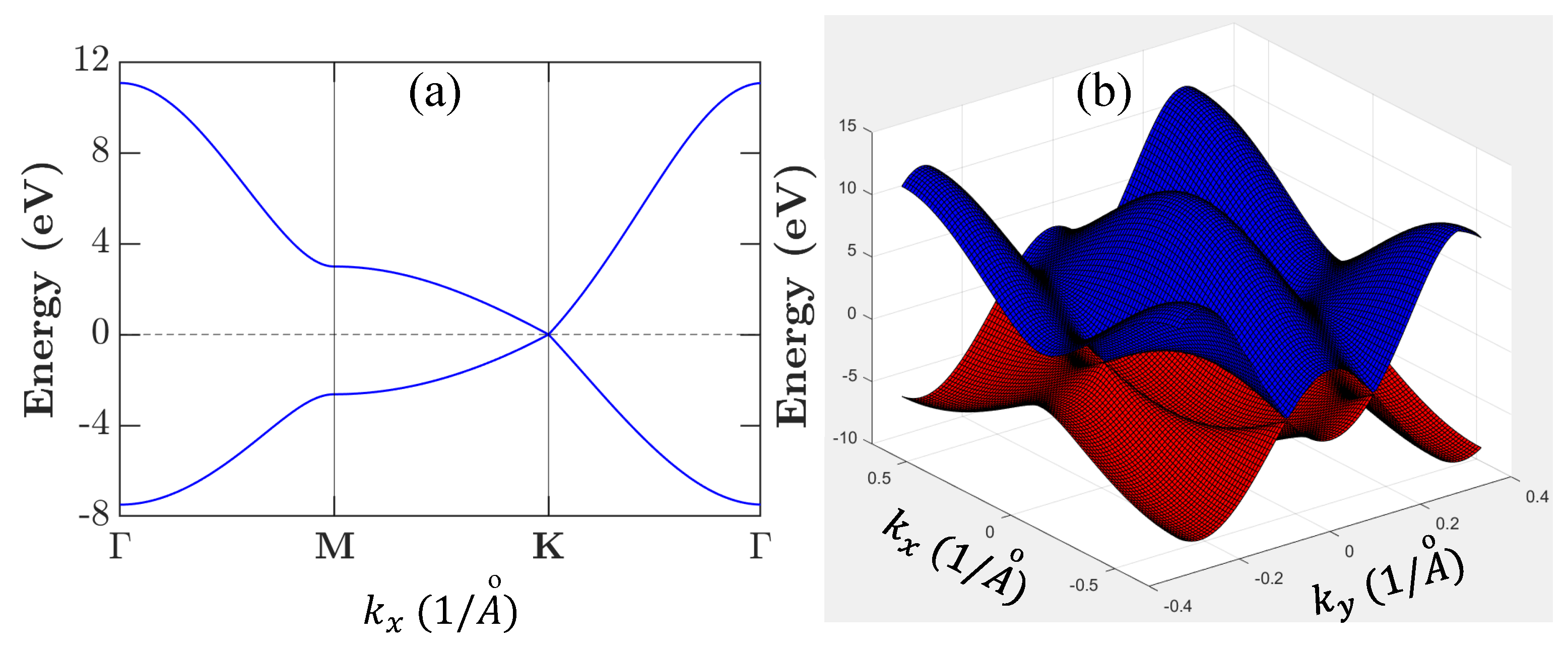
31) is plotted in
Figure 6 by employing the graphene structural parameters listed in
Table 3.
Furthermore, by using the result in Equation (
31), two elements of the eigenvector,
and
, are found to be
As known experimentally, both the nearest-neighbor (nn) overlap and the next-nearest-neighbor (nnn) hopping integrals are much smaller than the nearest-neighbor (nn) hopping integral. By neglecting some constants, the dispersion in Equation (
31) can be further simplified as
where
is the corrected hopping amplitude.
5. Coulomb Diagonal-Dephasing Rate for Optical Coherence in Undoped Graphene
The quantum coherence of electrons is associated with the off-diagonal elements of their density matrix. The presence of an external field can induce coherence between two quantum states of electrons if the field frequency matches the energy separation between the two relevant electronic states. Dephasing refers to a physics mechanism which recovers classical behavior from a quantum system, and it quantifies the time required for electrons to lose their field-induced quantum coherence. Diagonal-dephasing rate connects to the ways in which coherence caused by perturbation decays over time, and then, the system goes back to the state before perturbation [
1]. This is an important effect in molecular and atomic spectroscopy, and also in condense-matter physics of mesoscopic devices.
In order to demonstrate the significance of band-structure computation with a tight-binding model on dynamical properties of electrons in graphene, we first study Coulomb diagonal-dephasing (CDD) rate for induced optical polarization of thermally-excited electrons and holes around the Dirac point in an intrinsic (or undoped) graphene sample. For undoped graphene, conduction electrons can be introduced by a photo-excitation process [
8], giving rise to equal number of electrons and holes
, where
represents the areal density of photo-excited carriers. For non-equilibrium photo-carriers under a transverse optical field, its induced optical coherence in steady states decays [
1] with the sum of CDD rates
and
for electrons (e) and holes (h), respectively. These two rates determine the inhomogeneous line-shape of a resonant interband-absorption peak at
for vertical transitions of electrons with their kinetic energies
in valence and conduction bands.
As illustrated by Feynman diagrams [
3] in
Figure 7, the CDD rate
of electrons is calculated as [
1,
44]
where both spin and valley degeneracies are included,
represents the surface area of graphene sample, the first and second terms correspond to the left and right panels of
Figure 7, and both scattering-in and scattering-out contributions [
44] are taken into consideration in these two terms. Moreover,
in Equation (
34) stands for the kinetic energy of electrons (e) or holes (h), and
is the Fermi function for thermal-equilibrium photo-carriers with their chemical potentials
at temperature
T. Here,
are separately determined by following two equations for given
T, i.e.,
where both spin and valley degeneracies are included and
in our case. Furthermore, in Equation (
34),
is the Lorentzian line-shape function,
are inverse lifetime of unperturbed electrons or holes, and
.
In addition, we have introduced in Equation (
34), as well as in Equation (
40) below, the Coulomb-interaction matrix elements, given by [
56]
where
in Equation (
36) is the two-dimensional Fourier transformed Coulomb potential
including static screening,
represents the vacuum permittivity, and
is the average dielectric constant of the host material. Additionally,
stands for the inverse Thomas-Fermi screening length, and can be given by a semi-classical model as [
57]
where both spin and valley degeneracies have been included.
Furthermore, the introduced
in Equation (
36) with
represents the Bloch-function form factor, calculated as [
57]
where the Bloch functions
in Equations (
5) and (
22) have been employed. In Equation (
38),
represents the number of near-neighbor atoms within a unit cell,
stands for the lattice vectors of the near-neighbor atoms relative to the sublattice site
, and
are two column eigenvectors in Equation (
32) for
. The Wannier-function structure factor
in Equation (
38) is defined as
where
and
. In fact, Equations (
34) and (
36)–(
39) are the key results in this paper for connecting the calculated tight-binding wave functions and band structures to a quantum-statistical theory for graphene optical properties.
Similarly, as illustrated by Feynman diagrams [
3] in
Figure 8, the CDD rate
of holes takes the form [
1,
44]
Computationally, the
-electron band structure of graphite can be obtained by employing the nearest-neighbor tight-binding model [
58,
59]. For graphene, the reciprocal lattice in the wave-vector space also acquires the hexagonal symmetry, same as that in real lattice. Moreover, the low energy bands are found linear and isotropic near the corners of the first Brillouin zone or
K point. Such
K-point linear bands become essential for the low-energy (or small wave-number) excitation of electrons. The calculated energy dispersions by diagonalizing the
Hamiltonian matrix are given by [
58,
59]
where
eV is the hopping integral between the nearest-neighbor atoms,
Å is the C–C bond length, and signs ± represents conduction (+) and hole (−) bands, respectively. Meanwhile, the corresponding spinor-type Bloch wave functions are found to be
where as shown in Equation (
20),
and
are two sublattice Bloch functions built from the superposition of the periodic
orbitals, Ref. [
59] and
is the angle between the wave vector
k and
x-axis. As in Equation (
22), we can further express the
atomic orbital by means of a generalized hydrogen-like wave function, given by [
60]
where
is a normalization factor,
the Bohr radius, and an effective nucleus charge number
is
.
In particular, the structure factor introduced in Equation (
38) can be calculated explicitly as
where
for Bloch wave function. Moreover, the Bloch-function structure factor in Equation (
44) takes the form [
60]
where tight-binding function
is given by Equation (
43), and the signs (±) correspond to conduction (+) and valence (−) bands, respectively [
59].
For intrinsic graphene, we have chemical potential
[
61]. However, there is still a finite intrinsic areal density
due to thermal excitation of electrons and holes at finite temperatures
T. In fact, we find
at the
K valley or
. Here, the calculated CDD rates from Equations (
34) and (
40), respectively, for electrons
and holes
are presented in
Figure 9a at
K and in
Figure 9b at
K. Since
as
, the thermal occupations of electron and hole states will be limited mostly to wave numbers close to the
K valley due to their lower kinetic energies
around
, as seen in
Figure 6.
The Coulomb diagonal-dephasing rates
presented in
Figure 9a,b quantifies an amplitude-decay process of induced electron-hole optical coherence with wave vector
k by an optical field towards the state before external perturbation. Furthermore, the Coulomb off-diagonal-dephasing rates
reveals deformations of induced optical-polarization waves with different wave vectors
[
8].
Considering the fact that major occupations of electrons and holes are accumulated around
, we have
only if
k is large. As a result, we find from Equation (
34) that
at
since we require
for large
,
for small
q, and
for both large
q and
, which, however, cannot be satisfied simultaneously. Similar conclusion can also be drawn for the second term in Equation (
34), where we find
. Combining these two facts together, we expect that a dip will occur at
for the Coulomb diagonal-dephasing rate
, as seen in
Figure 9a. Moreover, the observed anisotropic energy dispersion in
Figure 6a along the
K-
M and
K-
directions directly leads to a staircase-like feature in
Figure 9a for both
and
. As temperature
T is raised from
K in
Figure 9a to
K in
Figure 9b, the thermally-excited areal densities of electrons and holes are increased with
; therefore, the Coulomb interaction (
) between electrons and holes, as well as the Coulomb interaction among electrons or holes, will be enhanced greatly. Consequently, we find that both
and
are enhanced by a factor of
, in addition to amplified depth of the dip at
. Furthermore, different structural factors in Equation (
39), corresponding to ± signs for conduction and valence bands, give rise to a slightly larger value of
in comparison with that of
, as well as different dispersion features around the
K valley for
and
. These two computed Coulomb diagonal-dephasing rates can be physically applied to the spectral [
32] and polarization [
1,
36] functions in order to study transport and optical properties of graphene material.
6. Carrier Energy-Relaxation Rate in Doped Graphene
In condensed-matter physics, the microscopic energy-relaxation time usually refers to a measure of the time it requires for one electron in the system to be significantly affected by the presence of other electrons, lattice vibrations, and randomly-distributed ionized impurity atoms in the system through an either scattering-in or scattering-out process mediated by electron-electron, electron-phonon and electron-impurity interactions, respectively. Since the microscopic energy-relaxation time is assigned to a specific electronic state, we are able to define a thermally-averaged energy-relaxation time through the diagonal density-matrix elements of electrons for all electronic states. In this way, one can reveal unique temperature dependence of this macroscopic energy-relaxation time and utilize it for simplifying the well-known Boltzmann transport equation within the relaxation-time approximation [
44].
By going beyond the intrinsic graphene samples, we would like to investigate further the impurity scattering of electrons in extrinsic (or doped) graphene materials. In parallel with the discussion on scattering rates in
Section 5, we present here the calculations for intraband-scattering of electrons by randomly-distributed impurities. Results for intraband-scattering of holes can be obtained in a similar way.
By using the detailed-balance condition, the microscopic energy-relaxation time
of electrons in the presence of randomly-distributed ionized impurities can be calculated according to [
44]
where the scattering-in rate for electrons in the final
state is
whereas the scattering-out rate for electrons in the initial
state takes the form
Here,
represents the areal density of ionized impurity atoms in the crystal, and
comes from the randomly-impurity scattering of electron in the second-order Born approximation [
48,
62]. Explicitly, the random impurity-interaction matrix elements are calculated as
where
is the charge number of ionized impurity atoms.
Substituting Equation (
49) back into Equation (
47), we obtain
Using the inverse microscopic energy-relaxation time in Equation (
46), we can further calculate the macroscopic thermally-averaged energy-relaxation time
as a function of temperature
T, yielding [
44]
Actually, the results in Equation (
46) and in Equations (
50)–(
52) demonstrate the approach for relating the computed tight-binding wave functions and band structures to graphene transport properties described by a many-body scattering theory. This calculated relaxation time in Equation (
52) can be employed for building up different orders of moment equations [
63] based on semi-classical Boltzmann transport equation [
6] under the relaxation-time approximation [
44]. Here, the zeroth-order moment equation [
63] grantees the conservation of conduction electrons and allows us to find the chemical potential of electrons, as in Equation (
35), for given areal doping density and temperature. Moreover, the first-order moment equation [
63] makes it possible to find transport mobility and conductivity [
64] for bias-field driven conduction electrons.
For doped graphene, we have Fermi energy
at low temperatures, Ref. [
61] where
represents the areal electron density from doping, i.e.,
for completely ionized doping atoms. For low temperatures with
, we have
or
, where
is a unity step function and
is the Fermi wave number.
Physically, the Coulomb diagonal-dephasing rates
in
Figure 9 describes a decay process of induced electron-hole optical coherence, which is induced by an optical field over time, towards the state before perturbation. On the other hand, the electron energy-relaxation rate
, determined by Equations (
46) and (
52), reflects the time, which is a quantum-statistical average over all occupied states of electrons, needed for recovering from a non-equilibrium-state occupation after an external perturbation to an initial thermal-equilibrium-state occupation before external perturbation via an elastic electron-impurity scattering process. Therefore, these two rates, as shown by
Figure 9 and
Figure 10, respectively, represent two fundamentally different microscopic physics mechanisms.
As seen from
Figure 10, we find the electron energy-relaxation rate
reduces with increasing temperature
T due to enhanced screening effect on Coulomb interaction
between two electrons or the rising of
in Equation (
37) with
T, which implies that we have to wait a longer time
for our system returning to its initial thermal-equilibrium state at an elevated temperature. Furthermore, using the second-order Boltzmann moment equation [
44], we would emphasize that this average energy-relaxation time
, as determined from Equations (
46) and (
52), is directly associated with the mobility of transport electrons limited by elastic scattering from existence of impurities in the system.
7. Conclusions and Remarks
In conclusion, by introducing a generalized first-principles quantum-kinetic model coupled self-consistently with Maxwell and Boltzmann transport equations, we demonstrate the importance to incorporate inputs from first-principles band-structure computations for accurately describing non-equilibrium optical and transport properties of electrons in graphene. Generally speaking, the physical properties of an active material in a device are determined by both underlined band structures of involved materials and non-equilibrium responses to various external impulses.
In this study, we initialize with the tight-binding model for investigating band structures of solid covalent crystals by means of localized Wannier orbital functions, and further parameterize the hopping integrals in the tight-binding model for different covalent bonds. After that, we apply the general tight-binding-model formalism to graphene in order to acquire both band structures and wave functions of electrons within the whole first Brillouin zone of two-dimensional materials. For illustrating their significance, we utilize them to explore the intrinsic electron-hole Coulomb diagonal-dephasing rates used for spectral and polarization functions of graphene materials, and meanwhile, the energy-relaxation rate from extrinsic elastic scattering by impurities for transport mobility of doped electrons in graphene.
Theoretically, our current theory is capable of first-principles calculations of ultra-fast dynamics for non-thermal photo-generated electron-hole pairs. Simultaneously, this a theory also enables to describe electromagnetic, optical and electrical properties of semiconductor materials all together, as well as their interplay. Technologically, in combination with first-principles band-structure computations, the numerical output of current first-principles dynamics model can be used as an input for material optical and transport properties and put into a next-step simulation software, such as COMSOL Multiphysics, for a target device. Consequently, device characteristics can be predicted accurately for numerical bottom-up design and engineering.


