1. Introduction
Recent technological developments transcending the vision of the Internet of Things (IoT) have created a huge global market for “smart” devices such as smart phones, televisions, tablets, watches and many more, which is forecast to grow exponentially over the next few years [
1]. Naturally, this progress goes in parallel with the demand for electronic components used in smart devices and in particular, in energy conversion and storage applications. While renewable energy resources are considered for clean and sustainable energy production around the world, solar cells are among the potential technologies that significantly contribute toward the present global energy demands and is anticipated to grow further in the future [
2,
3]. Both in solar cells and in most of the smart devices containing transparent displays or touch panels, one of the inevitable device stacks is the transparent conducting electrode (TCE). To date, indium tin oxide (ITO) has been ubiquitously employed as TCE in applications requiring high transparency and low sheet resistance. However, with the ever growing demand for TCEs, the scarcity of indium coupled with its cost and energy inefficient production methods and its poor durability in flexible electronic applications prompt the search for appropriate ITO alternatives [
4].
Many novel materials such as PEDOT:PSS [
5,
6], graphene [
7], carbon nanotubes [
8] and metal nanostructures [
9] with low sheet resistance (>1 Ω/□), high transmittance (>80%) in the visible region and high durability have been investigated as TCEs in various optoelectronic applications. Among these, metal nanostructures, in particular, metal mesh electrodes, hold additional promising features like intrinsic high conductivity, transparency in the visible and infrared region, low haze, surface plasmonic effect, high flexibility, and versatile and cost effective preparation strategies, which are best suited for photovoltaic applications [
9,
10]. For example, Ag nanowires/mesh electrodes are successfully demonstrated as TCEs in semi-transparent organic [
11,
12,
13] and perovskite solar cells [
14,
15], which in many instances outperform the ITO-based counter parts.
In general, the optoelectronic properties of the metal mesh/network-based TCEs are strictly governed by their geometric and dimensional features such as, (i) metal mesh line width; (ii) pitch size or void area between the subsequent conducting mesh lines and (iii) thickness of the electrode layer [
16]. With increasing metal mesh line width, electrical conductivity of the electrode increases and, concomitantly, transmittance decreases; whereas, the trend is reversed upon increasing the pitch size of the network structures. Similarly, increasing the metal electrode thickness reduces the overall sheet resistance, however, it also raises the surface roughness that creates additional shunt paths across the device stacks, impeding the device functionality. Further, the voids within the electrode mesh structure also cause an additional issue in solar cells as the charge carriers reaching these spaces are hardly collected by the electrodes. The lateral transport of charges across the void space towards the conducting mesh lines demands charge carrier diffusion length in tens of micrometer scale, which is not common in many solar cells. In such cases, the accumulated charges in the metal mesh void structures facilitate parasitic charge recombination events that reduce the overall photoconversion efficiency (PCE) of the solar cells [
13,
16].
To overcome the surface roughness and lateral charge collection issues, the metal mesh structures are often employed in combination with thin conducting filler layers in devices as hybrid electrodes. The filler layer ensures lateral charge collection from the electrode void area to the electrode conducting line; however, this field-driven drift process is accompanied with significant ohmic losses, which is undesirable in any applications, particularly for solar cells. Along these lines, a variety of conducting filler materials such as PEDOT:PSS [
15], zinc oxide [
13], Al-doped zinc oxide [
17] and TiO
2 [
18] have been tested in solar cells in combination with metal mesh electrodes, and a few such combinations have shown promising results.
As of now, the selection of a filler material for a metal mesh electrode is achieved based on the conventional figure of merit determined from the sheet resistance and optical transmission [
4]. Based on this, a few studies regarding optimizing the charge collection using metal grids in organic solar cells and their modules are reported [
19,
20]. Interestingly, in these examples and also during the regular selection of the filler layers, the ohmic losses incurred by the hybrid metal mesh TCEs are not considered and the corresponding influencing parameters are not investigated to the best of our knowledge.
In this work, we use a simple numerical model to determine the optimal hybrid metal mesh geometry for maximizing the current collection in a perovskite solar cell and elucidate its dependency on filler sheet resistance and its effective charge carrier extraction distance, which is a function of the metal mesh electrode pitch size. To verify the theoretical predictions, we fabricated hybrid metal mesh electrodes with well-defined honeycomb-shaped metal network structures with varying pitch size and two different filler materials with different sheet resistance values, and applied them as TCE in perovskite solar cells. The solar cells parameters show a clear reliance of filler sheet resistance on the effective charge carrier extraction distance, which is in line with our numerical model. Based on these results, our model is expected to form the basis for selection rules for TCE, in addition to the existing figure of merit, to fabricate efficient metal mesh electrode/filler combinations, especially for lateral charge collection.
2. Materials and Methods
2.1. Preparation of Honeycomb Shaped Au and Cu-Network Electrodes on Glass Substrates
Highly periodic, uniform Au-network structures with well-controlled geometric features were prepared on glass substrates using photolithographic technique. On precleaned, ozone treated glass substrates, photoresist LOR5B was spin cast at 5000 rpm for 30 s, followed by annealing at 180 °C for 7 min. Furthermore, photoresist S1813 was spin cast using the same parameters and annealed at 120 °C for 4 min. With the appropriate prepatterned mask on top, the substrates were exposed to ultraviolet (UV) light for 3 s using a mask aligner. Furthermore, the substrates were treated with MF318 solution for 20 s followed by thorough washing in deionized water. The developed substrates were transferred to a physical vapor deposition (PVD) chamber, where 4 nm chromium and 70 nm gold were evaporated successively. After, the substrates were left in a beaker with N-methylpyrrolidone (NMP) solvent overnight, and this was followed by ultrasonication for 4 min to remove all the photoresist. This results in well-defined honeycomb shaped Au-network electrodes on glass substrates. For Cu-network electrodes, the same procedure was followed except approximately 70 nm Cu was evaporated instead of Au in the PVD chamber.
2.2. Deposition of Low Temperature TiO2 (LT-TiO2) and Aluminum-Doped Zinc Oxide (AZO) Filler Layers on Metal Network Electrodes
Compact TiO2 layers of approximately 60 nm thickness were prepared on precleaned ITO (reference) and Au-network electrode substrates by spin casting a precursor solution containing 109 μL of titanium tetrabutoxide, 3.4 μL of 37% HCl and 3 μL of ethanol at 2000 rpm for 50 s, followed by annealing at 100 °C for 30 min in ambient conditions. The thickness of the TiO2 layers was adjusted to completely cover the metal network electrodes.
Approximately 70 nm thick aluminum-doped zinc oxide (AZO) layers were sputter deposited on ITO, Au-network and Cu-network electrode substrates in a Denton vacuum Explorer® system by employing confocal sputtering technique. A 2 wt% Al-doped ceramic target was used. The substrates were mounted on a stainless-steel holder, which was positioned 60 mm away from the target. The chamber was evacuated to a base pressure of 6 × 10⁻⁶ bar prior to the sputtering process and during sputtering, the pressure was maintained at 6 × 10⁻³ bar. The sputtering process was carried out with a radio-frequency (RF) power of 137 W for 9 min, and the substrate holder was continuously rotated to ensure the film uniformity.
The thickness of the prepared LT-TiO2 and AZO layers deposited on clean dummy glass slides was measured by using a profilometer. The same substrates were used to determine the sheet resistance of LT-TiO2 and AZO layers by using four-point probe technique, and the values are >1 G Ω/□ and 7000 Ω/□, respectively. The Rsh of the used ITO reference was determined as approximately 13 Ω/□.
2.3. Fabrication of Perovskite Solar Cells
All the starting materials for solar cell preparation were purchased from Sigma–Aldrich (St. Louis, MO, USA) unless otherwise specifically stated, and used as received. The hole transporting material 2,2′,7,7′-tetrakis-(N,N-di-p-methoxyphenylamine) 9,9′-spirobifluorene (spiro-OMeTAD) was purchased from Merck KGaA, Darmstadt, Germany.
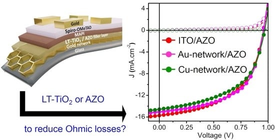
For CH3NH3PbI3 (MAPI) film deposition, 1 M PbI2 and methylammonium iodide were dissolved in dimethylformamide and stirred for at least 2 h at room temperature. To facilitate the substrate wetting properties of sputter prepared AZO layer, 60 μL of phenyl-C61-butyricacid (PCBA 0.1 mg/mL) in 1,2-dichlorobenzene solution was spin cast on AZO layer at 2000 rpm for 50 s. Once the MAPI precursor materials were completely dissolved, 80 μL of this solution was spin cast on LT-TiO2 and AZO substrates at 3000 rpm for 50 s. While the substrates started spinning, right after 8 s, 200 μL of toluene (orthogonal solvent) was continuously dripped onto the substrates. Furthermore, the substrates were annealed at 100 °C for 25 min on a hot plate inside a N2 filled glovebox, resulting in an approximately 400 nm thick uniform MAPI layer. Successively, a hole transporting layer was deposited onto the perovskite layer by spin casting a chlorobenzene solution of spiro-OMeTAD (72.3 mg/mL), 43.2 μL of 4-tert-butyl-pyridine (TBP), and 26.3 μL of LiTFSI (520 mg/mL in acetonitrile) at 2000 rpm for 50 s in the glovebox. These substrates were stored overnight in a dry box (relative humidity < 10%) to facilitate the air doping of spiro-OMeTAD layer. Finally, approximately 70 nm thick gold back contact was deposited in a PVD chamber, completing the solar cells. The active area of the fabricated devices is either 0.09 or 0.16 cm2 defined by the cross-section area of the bottom and top electrodes.
Characterization of the solar cells was carried out by using an Oriel solar simulator under AM 1.5, 1000 W m−2 conditions and a Keithley 2400 source meter. The current–voltage (I–V) curves were measured from +1.5 V to 0.5 V and back at the scan rate of approximately 130 mV s−1 under N2 atmosphere. The photovoltaic parameters such as Jsc, Voc, fill factor (FF) and PCE were determined from the corresponding I–V curves using a home-built software.
3. Results
One of the major advantages of metal mesh electrodes is their excellent transparency (>85%), which is a result of their geometry of thin conducting mesh lines with void spaces in between. With increasing distance between the successive metal mesh lines (pitch size), the transparency of the electrode structure improves linearly, making it appealing for transparent and semi-transparent optoelectronic applications. However, in devices that demand charge collection or injection into the void area such as solar cells or organic light emitting diodes (OLEDs), a trade-off between the transparency and conductivity is achieved by controlling the pitch size, and an addition of a conducting filler layer ensures the maximum lateral charge collection or injection, naturally, at the expense of voltage. The impact of such current and voltage losses on organic solar cells performance is addressed in a few reports. For example, Galagan et al. addressed the influence of electrode pitch size in hexagonally structured Ag nanowire grids [
19], whereas Jacobs et al. studied different possibilities for incorporating metal wires for improved charge collection in thin film solar cells [
21]. Cravino et al., studied the current contribution from neighboring regions around the active area of an organic solar cell by considering the distances between the electrodes and sheet resistance of the charge collecting layer such as PEDOT:PSS used in these devices [
22]. The consequences of designing charge collecting metal grids and associated voltage or current loss in modules have also been addressed [
20,
23]. In spite of these studies, a more realistic picture on ohmic losses in solar cells employing the hybrid metal mesh electrodes can be obtained by combining the sheet resistance (
Rsh) of the filler layer, overall charge carrier density in the device and the distance over which the charge carriers needs to be transported (
l) from the void area to the conducting metal mesh line. To address the voltage and current losses originating from the hybrid metal mesh TCE, we adopted a numerical expression similar to Cravino et al. [
22], which they used to estimate additional charge collection from neighboring regions in organic solar cells, and the expression is,
where Δ
V is voltage loss,
Rsh is sheet resistance of the filler layer,
Jsc is photocurrent density,
l is the distance over which the charge carrier needs to be transported through the filler layer (charge extraction length ≈ about half of the pitch size),
wel is the width of the metal mesh line and
wfiller is the effective width of the filler layer depending on the geometry as well as
wel value.
The solution for this expression can be derived using a model system. Consider a perovskite solar cell employed with a honeycomb metal mesh hybrid electrode showing the maximum
Jsc of 20 mA/cm
2. Here, the value of
wfiller is assumed to be 20
wel, since the pitch size is approx. 20 times the
wel value. Solving Equation (1) for the process of transporting a charge carrier located in the void at “
l” distance from the conducting mesh lines (as depicted in
Figure 1 inset) results in the plot of
l vs.
Rsh as shown in
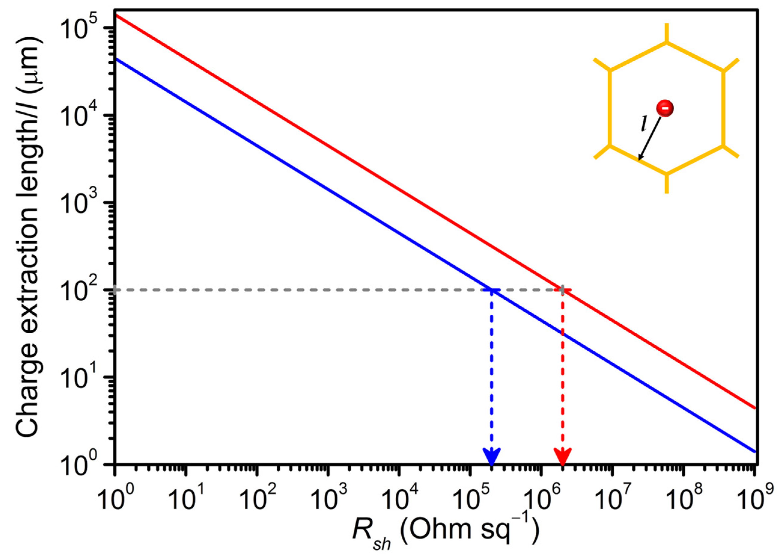
Figure 1 for the voltage loss of maximum 100 mV and minimum 10 mV.
The plot clearly shows the limitations of the possible combinations of
l and
Rsh for the anticipated voltage loss. For example, to extract a charge carrier from a distance of 100 µm at the expense of 10 mV, the filler should have the maximum
Rsh of 1 × 10
5 Ω/□ (blue dotted arrow). However, in the same device for the same
l value, if one can afford a 10-fold higher voltage loss (100 mV) then the filler with the maximum
Rsh of 1 × 10
6 Ω/□ (red dotted line) can be used to extract the charges. It is also clear from
Figure 1 that for the same filler layer (same
Rsh), with increasing
l, i.e., upon increasing the pitch size of the metal mesh nanostructures, the loss in voltage also increases. In other words, for each threefold increase in distance between the charge carrier and the conducting mesh line, a minimum of 10-fold higher voltage is required to extract this carrier to contribute to the device photocurrent. This is a significant loss for any high-performing optoelectronic devices, in particular, for perovskite solar cells.
On the other hand, reducing Equation (1) to obtain the relation between
Rsh vs.
l for the above mentioned model system results in:
which clearly evidences an inverse quadratic relationship between the filler
Rsh and
l value. This means, with an order of increase in
l value, i.e., for a metal mesh structure with an order of increased pitch size requires a filler layer with at least two orders of magnitude reduced
Rsh to collect a charge carrier with a same voltage loss value. In absolute terms, for the given conditions, a filler with a sheet resistance of 100 Ω/□ can effectively transport a charge carrier from a distance of approximately 4 mm with 10 mV loss in the voltage. If
l exceeds beyond 4 mm, to extract the charge carriers from a metal network void without losing further voltage, it is essential to use a filler with further reduced
Rsh. These findings are of paramount importance for solar cells as they assist in mitigating the additional parasitic ohmic losses by suggesting the maximum limit of
Rsh of the filler layer for a metal mesh structure with a specific pitch size. Interestingly, the plot also helps to predict the performance loss in any optoelectronic device based on the metal mesh electrode geometry and filler layer combination, prior to device fabrication.
To verify these theoretical findings, we prepared honeycomb-shaped Au-network electrodes on glass substrates with increasing pitch size and
wel using the photolithographic technique, in combination with two different filler layers showing significantly different
Rsh values.
Figure 2a–c show the lateral scanning electron microscopic (SEM) images of the prepared Au-network electrode structures along with their corresponding
wel and pitch size. The maximum
l value for the corresponding void spaces is equivalent to the distance between the center of the honeycomb structure and the middle of a metal mesh line, which can be obtained by determining the radius (r = a × √3/2) of inscribed circles in the hexagons, where “a” is the length of a side of the hexagon. The calculated
l values corresponding to the honeycomb network pitch size are also listed in
Figure 2a–c.
It is evident from the images that the prepared honeycomb Au-network structures are uniform and highly periodic with well-controlled geometry and dimensions, as a result of the photolithographic technique. Notably, the geometry fill factor of these metal mesh electrodes was maintained as 10% despite increasing the pitch size, by adjusting the wel accordingly (5, 10 and 15 μm). This ensures the same sheet resistance value for all the metal mesh structures irrespective of the pitch size. The influence of increasing l value as a consequence of network pitch size and Rsh of the filler layers on ohmic losses is evaluated by employing these metal nanostructures as hybrid TCEs in planar perovskite solar cells.
Using these nanostructured electrodes, two sets of planar perovskite solar cells were prepared by employing low temperature TiO
2 (LT-TiO
2,
Rsh > 1 G Ω/□) and Al-doped ZnO (AZO,
Rsh = 7000 Ω/□) as electron transport as well as conducting filler layers. An approximately 60 nm thick LT-TiO
2 layer was deposited on Au-network electrode on glass substrates by using sol-gel method, which is known to cover the electrode structure uniformly [
13]. On the other hand, approximately 70 nm thick AZO layer was prepared on Au-networks via the RF sputtering technique. The conformal coverage of Au-networks by AZO layer is clearly evidenced by the comparative cross-sectional SEM images of a glass substrate containing the Au-network structure before and after AZO deposition as shown in
Figure 2d,e.
The selection of LT-TiO
2 and AZO for this investigation was based on the similarity in their work function (≈4 eV) [
24,
25], which circumvents possible differences in contact resistance at the Au-network electrode/electron transport layer interface. Also, as shown in
Figure 2f, the transmittance of both LT-TiO
2 and AZO deposited Au network structures is quite comparable (80%) in the visible region, which safely neglects the possible light transmission differences as a reason for corresponding solar cells performance differences. This transmittance value is less than that of the conventional ITO TCE (85%) in the visible region [
13]. Further, the stark contrast in their measured sheet resistance values can lead to unambiguous conclusions regarding the correlation of
Rsh and
l of hybrid TCEs. For this reason, both the electrodes and filler layers are designed and prepared in a careful way that the possible differences in the solar cells performance can be attributed solely to the change in the
l value and
Rsh of the conducting filler layers.
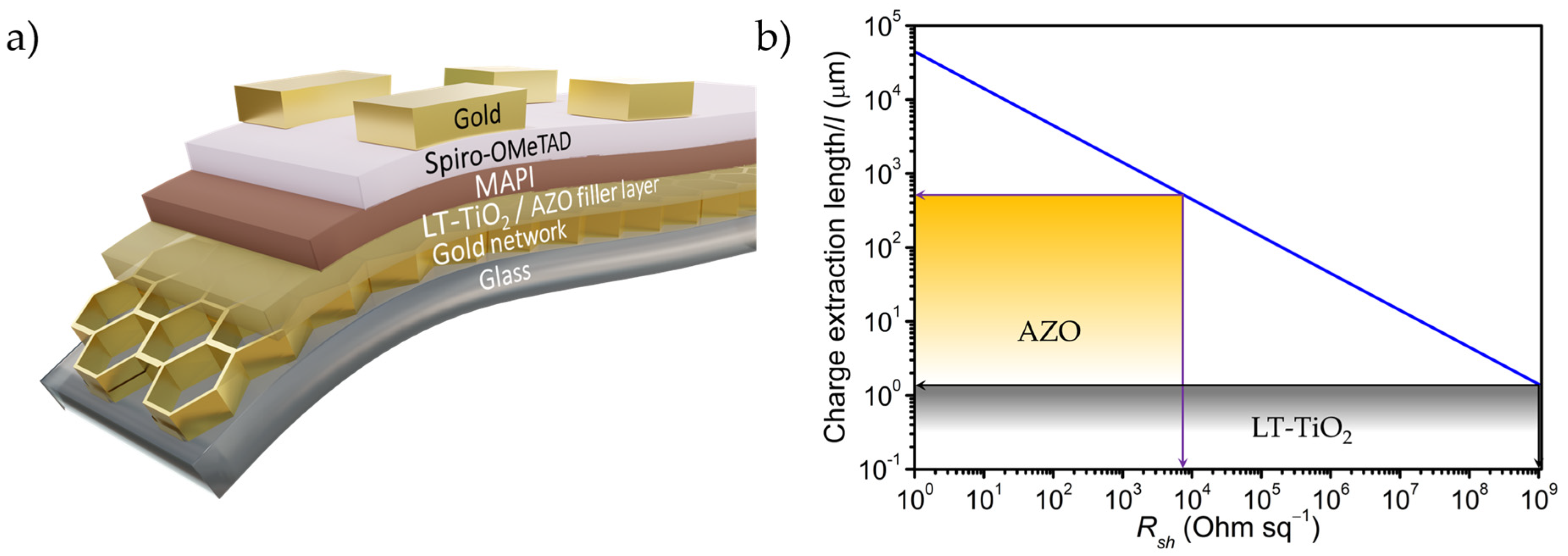
Furthermore, planar perovskite solar cells are fabricated on these conducting filler layers by successively depositing photoactive MAPI, hole transporting spiro-OMeTAD layer and gold top electrode (see Materials and Methods). The final device geometry is Au-network electrode/LT-TiO
2 or AZO/MAPI/Spiro-OMeTAD/Au and is schematically shown in
Figure 3a. In addition to the Au-network electrode-based solar cells, individual reference devices were also fabricated with ITO electrodes for LT-TiO
2 and AZO filler layers under similar experimental conditions.
Prior characterizing the solar cells, the maximum possible
l values, i.e., effective charge extraction length at the voltage loss of 10 mV for both LT-TiO
2 and AZO are deduced from
Figure 1 based on their
Rsh values, and are schematically shown in
Figure 3b. The plot indicates that the RF sputtered AZO (
Rsh ≈ 7000 Ω/□) can theoretically transport a charge carrier up to approximately 400 μm distance at the expense of 10 mV; whereas, due to very high
Rsh value (>1 G Ω/□) of the prepared LT-TiO
2, the corresponding maximum lateral charge transport distance is determined to be approximately 1 µm for the same voltage. The substantial difference in their effective charge extraction distance is expected to play a vital role in dictating the corresponding solar cell performance. Based on the solar cells results obtained using Au-network/AZO electrode, we also tested the viability of preparing a similar mesh using less expensive Cu instead of Au, applied it in combination with AZO and compared with the devices employing Au-network/AZO hybrid electrode.
The solar cells were mechanically sealed in test chambers under nitrogen atmosphere and characterized for their photovoltaic features. The measured current–voltage (I–V) curves for solar cells prepared on Au-network electrodes with varying pitch size in combination with LT-TiO
2 and AZO filler layers and corresponding ITO reference devices are exhibited in
Figure 4. The determined parameters from the respective I–V measurements are collected in
Table 1.
It should be noted that the prepared perovskite device stacks are not optimized for the maximum PCE. Nevertheless, they are employed in these studies as testbeds due to the excellent photovoltaic properties of MAPI, known for high and similar photocarrier density in all the prepared devices, which is one of the essential criteria to derive the relationship shown in
Figure 1 and
Figure 3. On the other hand, the ease of preparation and high reproducibility of the corresponding photovoltaic parameters of the planar perovskite solar cells enable investigating the impact of intrinsic changes in one of the device stacks on device performance [
26]. Therefore, the main discussion is restricted to the relative differences in the photovoltaic parameters of the devices with increasing Au-network pitch size and different filler layers.
4. Discussion
Figure 4a,b display the measured I-V curves of the perovskite solar cells prepared on Au-network hybrid TCEs with LT-TiO
2 and AZO filler layers, respectively. Considering the Au-network/LT-TiO
2 based perovskite solar cells, they exhibit photovoltaic character, however, the determined
Jsc,
Voc and fill factor (FF) values are remarkably poor, irrespective of the Au-network pitch size (
Table 1). On the other hand, with increasing Au-network pitch size from 97 to 293 μm, the
Rs value of the respective perovskite solar cells linearly increases from 1500 to 4500 Ω·cm
2 and
Rshunt also increases relatively. This emphasizes the influence of Au-network pitch size on device performance upon employed with a poorly conducting filler layer such as LT-TiO
2. The reference solar cells (
Figure 4c) prepared with LT-TiO
2 on ITO electrode (ITO/LT-TiO
2) also show
Rs and
Rshunt values comparable to a device with the Au-network/LT-TiO
2 TCE (97 μm pitch size,
Table 1), however, it displays
Jsc of 11.7 mA/cm
2,
Voc of 0.99 V and FF of 56% resulting in an overall PCE of 6.5%, which is comparable with the solar cells containing LT-TiO
2 prepared using a similar method [
27]. This clearly suggests that the device stacks in Au-network/LT-TiO
2 TCE-based solar cells are not limiting the performance. On the other hand, the calculated maximum allowable
l value for LT-TiO
2 (approximately 1 µm) based on its
Rsh is exceeded well in all the prepared Au-network electrode structures under investigation. This is anticipated to result in poor lateral charge extraction by LT-TiO
2 towards the metal mesh lines, and consequently leads to charge carriers’ accumulation and recombination at the electrode/LT-TiO
2 interface and poor
Jsc,
Voc and PCE values. Furthermore, upon comparing the photovoltaic parameters of the devices within the same series, both
Jsc and
Voc considerably increase with decreasing
l value from 141 to 44.3 µm in the hybrid TCEs resulting in 2–3 fold higher PCE values. These experimental observations are in line with the predictions based on our numerical model.
In the case of Au-network/AZO-based hybrid electrodes, the calculated effective charge carrier transport distance (400 µm) of the filler layer is well above the
l values corresponding to the Au-network structures used. Thus, theoretically, AZO is expected to effectively extract all the photogenerated charge carriers from the Au-network electrode void space without significant ohmic losses. In fact, all the perovskite solar cells prepared on Au-network/AZO hybrid TCEs display comparable photovoltaic parameters including
Rs and
Rshunt values with those of the ITO/AZO based reference device (
Figure 4b,c, and
Table 1). With increasing
l from 44.3 μm (pitch = 97 µm) up to 141 μm (pitch = 293 µm) in Au-network/AZO-based devices,
Jsc is maintained at approximately 15 mA/cm
2 with a slight fluctuation in
Voc. Interestingly, unlike the devices prepared on Au-network/LT-TiO
2 TCEs, the
Rs and
Rshunt values of the respective solar cells remain comparable irrespective of the Au-network pitch size (
Table 1), suggesting the influence of the conducting filler layer. The fact that there is no current collection loss up to a pitch size of 293 µm is in full agreement with our model, which allows the charge extraction of up to 400 µm for a 10 mV drop. We still observe a slight decrease in
Voc and FF as the pitch size is increased to 293 µm, which could be due to: (i) shunt loss originating from device stack preparation steps, and/or (ii) the effective charge carrier extraction distance of AZO is overestimated as the plots in
Figure 1 are derived by using the upper limit of
Jsc,
wel and
wfiller values, and/or (iii) occurrence of charge carrier recombination events at the perovskite/electron transport layer interface, which generally reduces the
Voc and FF [
28].
Using this same strategy, we tested if Earth-abundant and less expensive copper grids in combination with AZO can be used as a hybrid TCE in perovskite solar cells.
Figure 4c showing the measured I–V curves of perovskite solar cells containing ITO/LT-TiO
2 and ITO/AZO reference electrodes, and Au-network/LT-TiO
2, Au-network/AZO and Cu-network/AZO hybrid TCEs with the pitch size of 196 μm and the determined corresponding photovoltaic parameters listed in
Table 1 indicate similar photovoltaic behavior of hybrid Cu-network/AZO based solar cells without any loss in the current collection. This first result is promising and opens the possibility of exploiting the combination of copper grid electrodes and a variety of appropriate filler layers as hybrid TCEs for semi-transparent perovskite solar cell applications.


 ,
, 


