Review

A Review on Rhenium Disulfide: Synthesis Approaches, Optical Properties, and Applications in Pulsed Lasers

by
Mahmoud Muhanad Fadhel
,
Norazida Ali
,
Haroon Rashid
,
Nurfarhana Mohamad Sapiee
,
Abdulwahhab Essa Hamzah
,
Mohd Saiful Dzulkefly Zan
,
Norazreen Abd Aziz
and
Norhana Arsad
*
Department of Electrical, Electronic and Systems Engineering, Faculty of Engineering and Built Environment, Universiti Kebangsaan Malaysia, UKM, Bangi 43600, Malaysia
*
Author to whom correspondence should be addressed.
Nanomaterials 2021, 11(9), 2367; https://doi.org/10.3390/nano11092367
Submission received: 20 August 2021 / Revised: 6 September 2021 / Accepted: 9 September 2021 / Published: 12 September 2021
(This article belongs to the Special Issue Nanomaterials for Photonics: Advances and Applications)

Abstract

:
Rhenium Disulfide (ReS2) has evolved as a novel 2D transition-metal dichalcogenide (TMD) material which has promising applications in optoelectronics and photonics because of its distinctive anisotropic optical properties. Saturable absorption property of ReS2 has been utilized to fabricate saturable absorber (SA) devices to generate short pulses in lasers systems. The results were outstanding, including high-repetition-rate pulses, large modulation depth, multi-wavelength pulses, broadband operation and low saturation intensity. In this review, we emphasize on formulating SAs based on ReS2 to produce pulsed lasers in the visible, near-infrared and mid-infrared wavelength regions with pulse durations down to femtosecond using mode-locking or Q-switching technique. We outline ReS2 synthesis techniques and integration platforms concerning solid-state and fiber-type lasers. We discuss the laser performance based on SAs attributes. Lastly, we draw conclusions and discuss challenges and future directions that will help to advance the domain of ultrafast photonic technology.

Graphical Abstract

1. Introduction

Ultrafast laser technology pertains to the creation, amplification and operation of ultrashort pulses with periods ranging from nanosecond to picosecond and femtosecond. Numerous distinct characteristics of pulsed lasers such as greater peak intensity, broad spectrum and fast temporal resolution [1] have driven a wide-range of uses such as laser welding and drilling [2], ultrafast spectroscopy [3,4] and frequency comb metrology [5,6]. Furthermore, pulsed lasers based on intensity modulation have proven their significant efficiency within a wide variety of distributed optical fiber sensors (DOFS) [7,8,9,10,11]. These kinds of lasers could be produced either by Q-switching or mode-locking methods, which are categorized into passive or active modulation methodologies. Typically, the Q-switching method can provide immense short-duration pulses in the microsecond to nanosecond range by regulating cavity loss frequently using a kilohertz-range frequency. On the other hand, the mode-locking method [12] comprising a concurrent in-phase lock of all the longitudinal modes in the cavity is frequently employed for producing extremely-short pulses ranging from a few femtoseconds to several picoseconds. Furthermore, the mode-locked pulse repetition rate is quite higher compared to the Q-switching repetition rate [13].
The active modulation technique relies on an optical modulator with an externally-applied modulating signal; the modulator is usually based on the electro-optic or acousto-optic effect [1,14]. Even though this methodology is quite robust, it fails to create very short pulses because of the inadequate bandwidth of active modulators. Conversely, passive modulation designs are in a position to offer quite shorter pulses, as the SA (saturable absorber) with a brief recovery time can regulate the cavity loss much quicker compared to an electronic optical modulator [15].
The saturable absorbers in passive Q-switching and mode-locking approaches could be generally split into two classes: real SAs, materials which demonstrate an intrinsic nonlinear drop in absorption with growing light intensity; and artificial SAs, devices which manipulate nonlinear effects, such as nonlinear polarization rotation (NPR) and nonlinear amplifying loop mirror (NALM), to simulate the action of a real SA by provoking an intensity-dependent transmission [16]. Nevertheless, NPR and NALM face several issues, such as high saturable threshold power and polarization sensitivity [17].
The advancements in microfabrication and material science have driven a growing number of materials which could be utilized as real SAs. Figure 1 depicts the progression of real SA technologies and their applications as photonic devices. In 1964, “reversibly bleachable” dye [18] and colored glass filters [19] were used for the first-ever presentation of SA-based pulse generation by Q-switching a ruby laser, just four years after Maiman demonstrated laser operation [20]. Reversibly bleachable dyes were extensively deployed to mode-lock lasers, driving the first exhibition of continuous-wave (CW) mode locking [21]. Later in 1983, ion-doped fiber has emerged as gain medium, and unstable mode-locking of a Nd:Fiber laser was reported using a dye SA [22]. It was quite challenging to create steady mode-locked pulses among fiber lasers, till the exhibition of semiconductor saturable absorber mirror (SESAM) in 1992 [23], a discovery which facilitated the first display of a passively mode-locked fiber laser (Nd:YLF) minus Q-switching instabilities. However, producing SESAMs typically comprises sophisticated and highly specialized instruments. Post-growth ion insertion or the uses of low temperature growth are employed for minimizing device response time. Additionally, a typical SESAM-based instrument operates in a narrow wavelength band (<100 nm) [1].
Unfortunately, such traditional SA materials have certain disadvantages, and therefore are not able to fulfill the main SA requirements, such as fast response time, strong nonlinearity, low loss, broad bandwidth, greater power handling and low costs [30]. SA material with nanometer-scale dimensionality may offer pronounced optoelectronic characteristics and powerful quantum confinement [31]. In 1997, zero-dimensional quantum dots (QDs) were used for pulse generation [32]. This presentation led to widespread interest in nanomaterial SAs. One-dimensional single-walled carbon nanotubes (SWCNTs) [33] and two-dimensional graphene [34] were regarded as potent materials for creating ultrafast pulses in the sub-picosecond range [30]. Usually, nanotubes with distinct diameters and chirality are tough to synthesize [35].
Apart from graphene, which was originally found in 2004 [36] with zero-bandgap structure, there are a broader category of novel 2D materials such as topological insulators (TIs) [37,38], transition metal dichalcogenides (TMDs) [39,40], black phosphorus (BP) [41,42], MXenes [43], antimonene [44,45], bismuthine [46,47,48] and tin selenide [49]. Nowadays, 2D materials are a preference for research and use in nearly each domain of science and engineering, especially TMDs which demonstrate adaptable chemistry. TMDs having MX2 chemical formula typically comprise a plane having hexagonally-placed transition metal atoms M (groups 4–10) in Figure 2 placed between two chalcogen atom-based hexagonal planes X (e.g., S, Se, Te). The M-X bonds within layers are mostly covalent, while weak Van der Waals forces hold the sandwiched layers [50]. TMDs have been acknowledged since the 60 s, and a set of 40 TMDs and their elementary attributes was reviewed in 1969 [51].
Recently, Rhenium disulfide (ReS2) in group 7 has been drawing the highest attention recently due to its uncommon electro-optical, structural and chemical attributes [52]. Contrasting to group 6 TMDs which steadied in extremely symmetric 2H structures, ReS2 possesses a distinctive distorted 1T structure that renders an in-plane anisotropy to its physical attributes [53]. Furthermore, because of the exceptionally weak interlayer coupling, bulk ReS2 functions as vibrational and electronically decoupled monolayers, causing a noticeable layer-independent character in different attributes [54]. Such unique attributes of ReS2 have encouraged several evolving applications such as catalysis, energy storage, optoelectronic devices and sensing [55,56,57]. Considering the strong light absorbance in a wide wavelength band, ReS2 material is potentially useful for optical modulation as required for pulsed lasers using SAs [58,59].
Report about the nonlinear saturable absorption response of ReS2 beyond its bandgap were first appeared in the literature in 2017 [60]. Yudong Cui et al. studied the optical response of ReS2 at around 1550 nm with the help of D-shaped fiber. The material was produced via chemical vapor deposition (CVD) method. However, this production method is complex and expensive. Later, much simpler and low-cost methods were used to synthesize ReS2 such as mechanical exfoliation (ME) [61] and liquid phase exfoliation (LPE) [62]. Along with saturable absorption response, investigating the large third-order nonlinear effect of ReS2 has enabled the generation of harmonic mode-locking lasers with high repetition rates pulses. Most of the reported ReS2-based SAs are made of solution using LPE method and deposited on fiber platforms such as the fiber ferrule [63,64,65] and microfiber [66,67] or on substrates such as sapphire [62,68,69,70] and quartz [71].
Here, we review the latest developments on generating short laser pulses using saturable absorbers based on ReS2. In Section 2 we mainly introduce the fundamental structure of ReS2 and its optical properties. Followed by the material fabrication methods and integration in free-space and fiber laser systems. In the last section we discussed the laser performance based on several parameters such as material thickness, SA modulation depth and optical damage threshold. On the basis of these developments, a conclusion and point of view for new prospective opportunities for ultrafast photonic technologies are emphasized.

2. Structure of ReS2 and Its Synthesis Methods

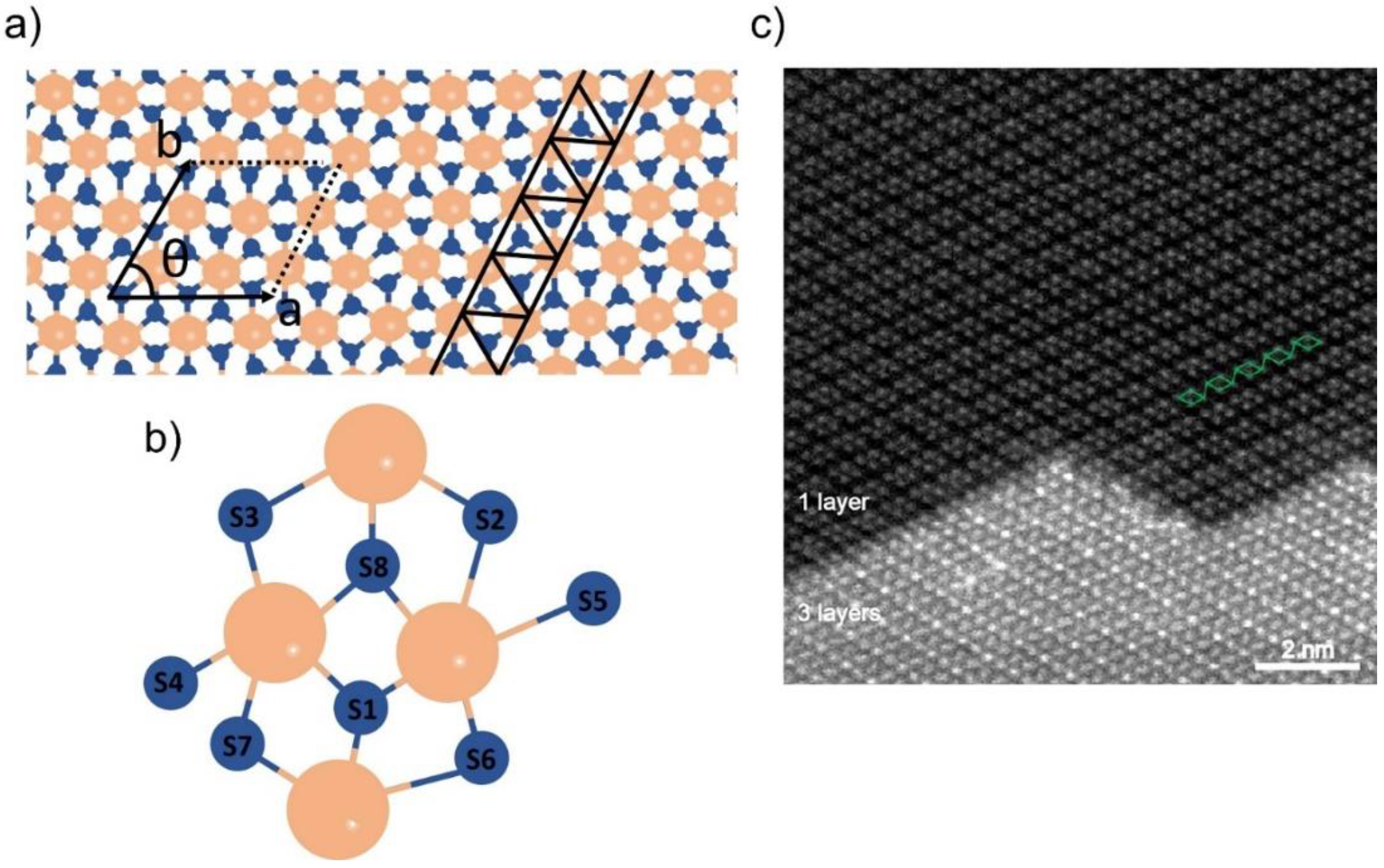
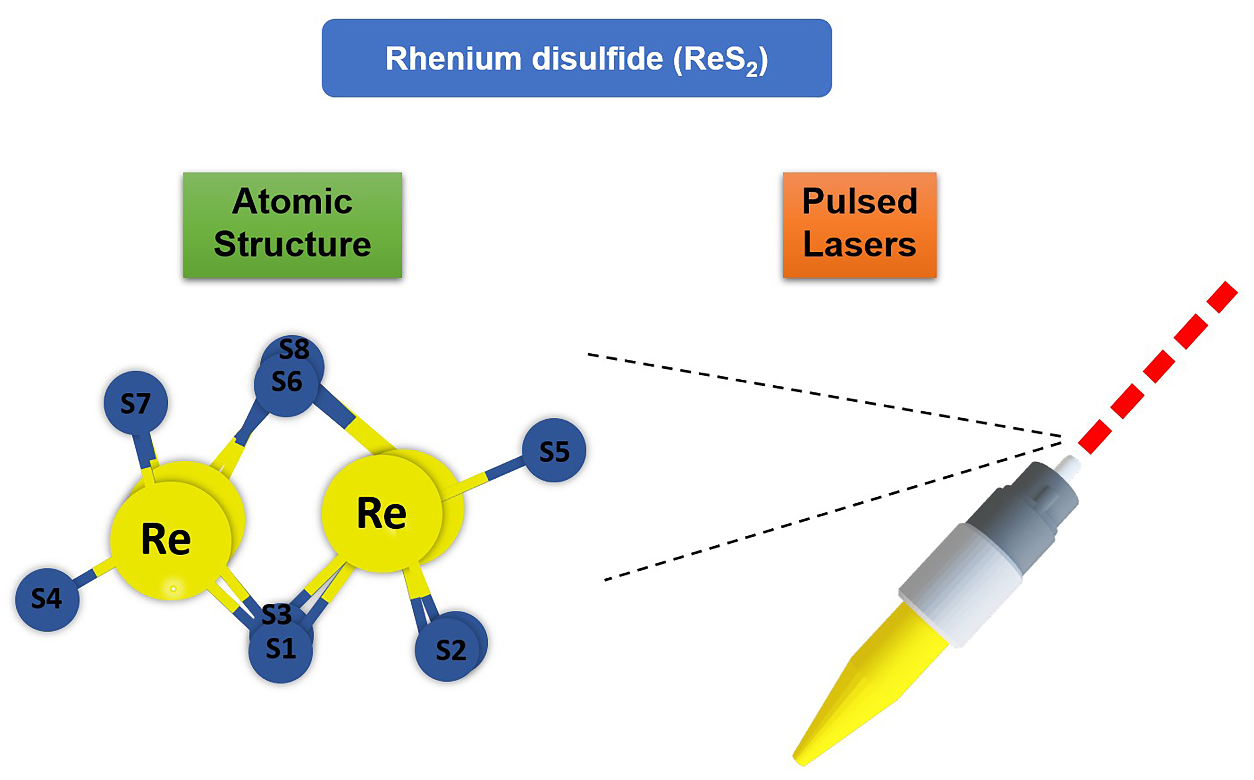
2.1. Rhenium Disulfide (ReS2)

Noddack, Tacke and Berg [72] were the first to discover rhenium in 1925, the last steady element in the periodic table [53]. The atomic arrangement of a ReS2 layer may be understood as a distorted 1T arrangement. The layer comprises a zigzag Re-Re chains along the b-axis of the lattice (Figure 3a) [54]. Metal-metal bonding causes doubling on the ReS2 unit cell, which, therefore, comprises eight S and four Re atoms (Figure 3b). Figure 3c depicts a less zoomed ReS2 annular dark field (ADF) picture showing tri- and monolayer regions on the flakes [73]. The ADF image clearly shows single layer regions comprising four Re atoms forming diamond-shaped links (green line).
ReS2 has a noteworthy aspect: the band structures for monolayer, trilayer and five-layer ReS2 are similar (Figure 4), indicating the nature of ReS2 of maintaining a direct-bandgap [74]. On the other hand, several TMDs have direct and indirect bandgaps in monolayer and bulk forms, respectively [54]. Bandgap characteristics can cause thickness to affect TMD properties extensively. Furthermore, based on the strain as well as ribbon width, the bandgap and electronic properties of mono-layered TMDs will alter greatly [75,76]. Ab initio calculations indicate that ReS2 bandgap does not change significantly when the thickness is increased from monolayer (1.44 eV), trilayer (1.4 eV) to five-layer (1.35 eV) [74]. This distinct response can be attributed to the absence of interlayer registry and weak interlayer connection caused by Peierls distortion of the ReS2 1T arrangement [54]. Additionally, the comparability of optical and electrical characteristics of single-layer and bulk ReS2 indicates that the material could offer a base to evaluate 2D system mesoscopic physics without facing the challenge of producing thick monolayer flakes with substantial area [67].
ReS2 in bulk form has anisotropic optical characteristics that are recorded [77]. The present emphasis is on the material comprising few layers and the monolayer structure [69]. Figure 5a depicts the photoluminescence (PL) spectrum of ReS2 flakes with diverse quantity of layers [78]. Thinning of ReS2 material form 7-layer to monolayer thickness is associated with a reduction in PL intensity. However, the red-shift associated with the peak position is insignificant, indicating little dependence on layer count. This observation is in agreement with theoretical bandgap calculations of ReS2 [52].
The ReS2′s Raman response is shown in many research works [79,80,81]. Due to the low symmetry of ReS2, a higher number of Raman modes could be seen as against the traditional TMDs. Additionally, the frequency shift for every Raman mode indicates minute changes concerning monolayer to bulk ReS2, as shown in Figure 5b; the figure indicates 18 Raman modes corresponding to bulk, five-layer and monolayer ReS2 [74]. There are six Raman modes with labels; these comprise two Ag-like low-frequency modes (identified at 136.8 and 144.5 cm−1) specific to out-plane Re atom vibrations. Furthermore, four Eg-like modes are observed (identified at 153.6, 163.4, 218.2 and 238.1 cm−1) specific to in-plane Re atom vibrations. The remaining Raman modes possess high frequency and are specific to relatively light S atoms [80]. Thus, one can determine the thickness of few-layer ReS2 by analyzing the Raman peak positions, much akin to the approach utilized for MoS2 [82].

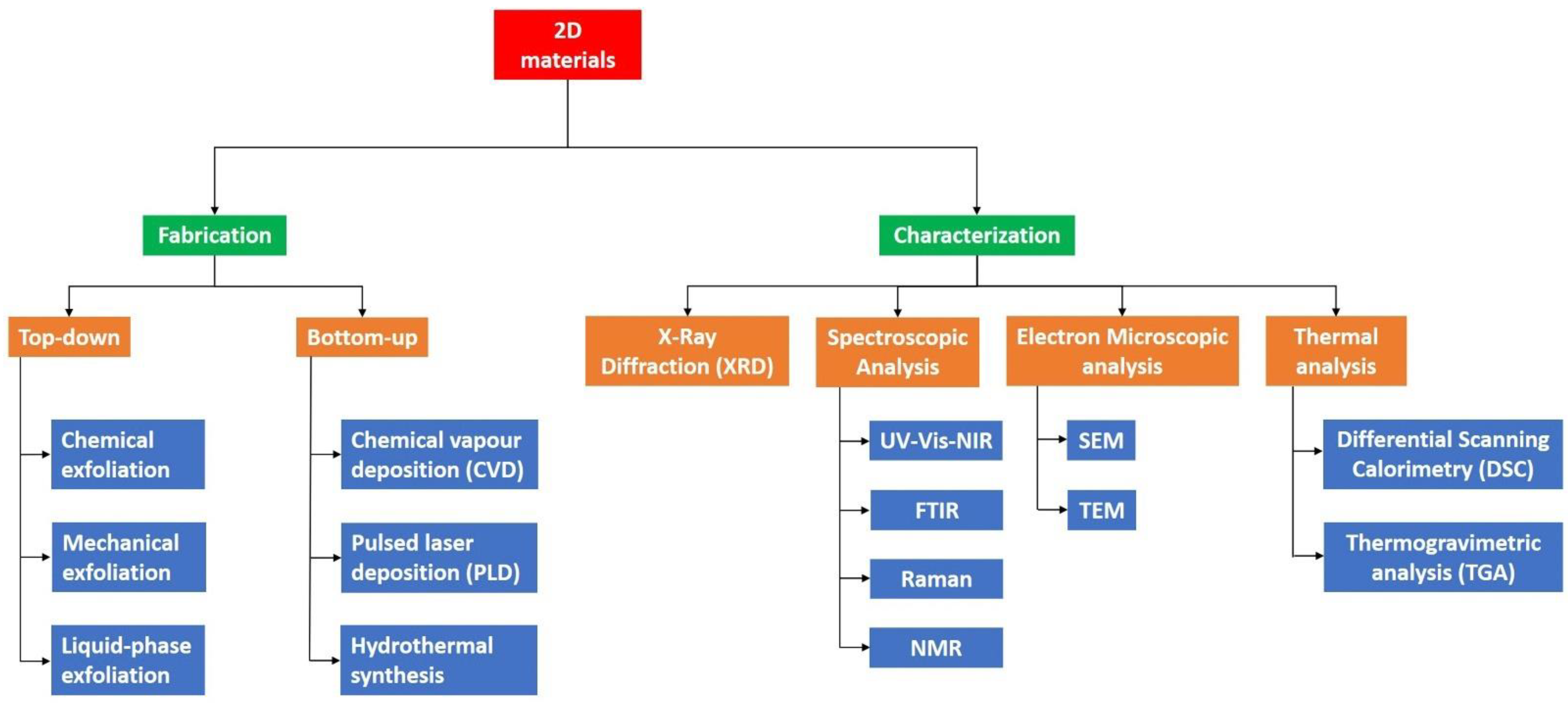
2.2. Synthesis Techniques

The systematic fabrication of 2D ReS2 with suitable size, thickness, morphology and crystal quality is substantially important for the exploration of their electronic, optical and thermal properties for prospective applications. Rhenium (Re) retains one of the highest melting points (~3180 °C) among all transition metals whereas disulfide is comparatively low (~155 °C). The large difference in melting points makes it considerably challenging to grow ReS2 thin films. This section summarizes the various fabrication techniques of ReS2. First part highlights the top-down synthesis approach which comprises of mechanical and liquid phase exfoliations. Subsequent part discusses bottom-up techniques which includes the physical vapor deposition (PVD), chemical vapor transport (CVT) and chemical vapor deposition (CVD) techniques [52]. Depending on the applications’ need, various characterizations can be performed for the 2D TMD ReS2 films. Figure 6 encapsulates the various fabrication and characterization techniques commonly used for 2D TMD ReS2.

2.2.1. Mechanical Exfoliation (ME)

Mechanical exfoliation has an outstanding influence on study and use of 2D materials on their fundamental characteristics. 2D graphene films were first acquired by Novoselov et al. [36] using the scotch tape method scientifically known as the mechanical exfoliation technique. It offers crucial access to high-quality flakes with good mechanical and electrical characteristics in spite of the inexpensive and coarse method [83,84,85,86]. A single crystal of bulk material is affixed to the adhesive side of the scotch tape and subsequently an additional piece of tape is positioned on the opposite side of the bulk material. Afterwards, both pieces of tape are peeled for numerous times. A clean and flat substrate, usually SiO2/Si (300 nm) is then used to affix the freshly sliced thin flake from the scotch tape. Similarly, mono or few layers can be obtained and transferred to the targeted substrate [52]. A highly responsive phototransistors using few layers of ReS2 is demonstrated by Liu et al. [87] using mechanical exfoliation approach. Figure 7 reveals the usual optical images of ReSe2 and ReS2 on SiO2/Si substrate with various layers exfoliated from the bulk materials [88]. However, the shortcomings of this method cannot be overlooked. It may produce edges and ribbons beside crystallographic directions. In addition, edges, number of layers and morphology are intense, owing to coarse procedure [89].

2.2.2. Liquid Phase Exfoliation (LPE)

Liquid phase exfoliation is an effective technique for exfoliating ReS2 nanosheets in large capacity without losing crystal quality. Currently, ReS2 exfoliation can be classified into two main types; sonication assisted exfoliation and ion intercalation exfoliation [90]. Hersam et al. has reported the ReS2 exfoliation via layer-by-layer isopycnic density gradient ultracentrifugation sorting of high density nanosheets in aqueous surfactant solutions [90]. At first, ReS2 powder in deionized water was sonicated with the amphiphilic small molecule surfactant sodium cholate. Subsequently, centrifuged at 7500 RPM to remove the unexfoliated flakes and the supernatant was collected. To precipitate large size ReS2 nanosheets, it was further centrifuged at 20,000 RPM. Finally, the comparatively uniform ReS2 nanosheets were attained with average thickness of around 3 nm and 50–100 nm of lateral size. A mixed solvent strategy was demonstrated using the Hansen solubility theory to prepare few layers of ReS2 nanosheets by exfoliating bulk ReS2 in an ethanol-water mixture [91]. It was reported that using a mixture of solvent with 72% deionized water and 28% ethanol for sonication is optimum to efficiently exfoliate large scale nanosheets of ReS2 with an average lateral size of 2.3 nm and a thickness of 50–80 nm. Colloidal ReS2 nanosheets for antitumor therapy and bioimaging applications using a sonication assisted liquid exfoliation method are also reported by Miao et al. [92].
Another technique to prepare ReS2 nanosheets is ion intercalation exfoliation. In this method, the cation, e.g., Na+, Li+, K+, with small ionic radius can easily insert into the interspace of layered bulk crystals. It expand the interspace drastically and weaken the Van der Waals forces between contiguous layers [52]. Another technique concerning the reaction of ReS2 powder with lithium borohydride (LiBH4) is developed to replace the conventional protocol requiring butyl lithium solution to effectively exfoliate ReS2 nanosheets [93]. Nevertheless, the obtained ReS2 nanosheets with respect to thickness, and lateral size are polydisperse. A homogeneous monolayer ReS2 film at large scale is challenging. Furthermore, certain solvents and reagents may cause contamination. In this perspective, the nanosheets obtained by this technique are more suited to biological and energy conversion applications [52].

2.2.3. Physical Vapor Deposition (PVD)

Physical vapor deposition method is a controlled environmental growth process. The liquid or solid precursors are evaporated in the form of molecules, or atoms in the presence of a low gas pressure within the high vacuum environment to the targeted substrate [94,95]. Synthesized high quality and large area ReS2 thin film on top of SiO2/Si substrate is obtained by using ReS2 powder (99% pure by Alfa-Aesar) with a cost effective, controlled and simple PVD method as reported by Qi et al. [96]. Before pumping the 1-inch quartz tube to vacuum, ReS2 powder is placed in the middle of the tube and then filled with argon (Ar) gas as depicted in Figure 8a. The temperature of the furnace is set to 900 °C. After one hour of ReS2 growth, the furnace is left to naturally cool down. The AFM is used to measure the thickness of ReS2, and a homogenous film of 2.30 nm thickness (three monolayers) is reported. Subsequently, the crystalline structure and morphology is studies using TEM and SEM, respectively. From the SEM image presented in Figure 8b, the surface of ReS2 film is found in micrometer size with continuous and clean surface. The as-grown ReS2 film is observed in nanometer size from the TEM image presented in Figure 8c. The average grain size is reported to be approximately 250 nm and dark-field TEM (DF-TEM) image is revealed in the inset of Figure 8c. However, higher melting point of the precursor and higher vacuum conditions may be the demerits of this technique for possible adaptability [52].

2.2.4. Chemical Vapor Transport (CVT)

Another highly popular approach for synthesis of bulk or single crystals of ReS2 and ReSe2 is the chemical vapor transport (CVT) technique. In this method, a sealed ampoule tube is used as the growth chamber, the precursor material and transport agent are placed inside the tube for several to 10 days under low pressure and high temperature [97]. The halogen (I2 or Br2) is used as the transport agent to aid the growth of ReS2 crystals [73]. Nevertheless, this causes the involuntary background doping and the properties of ReS2 crystals are also changed [89]. A study reported by Bhakti et al. [98] synthesized high quality ReS2 and ReSe2 crystals by employing the pure Re and S/Se powders without using halogen transport agent. The growth took place in a cleaned quartz tube at an appropriate temperature using Re and S elements. The shiny plate-like crystals with 20–100 microns thickness is witnessed by optical and SEM image as revealed in Figure 9.
Lei Xing et al. has recently developed a new approach by meticulously tuning the growth kinetics for direct synthesizing of thin ReSe2 flakes. The quartz ampoule is specially designed with a neck to separate the powders from the targeted substrate as shown in Figure 10a. This modified method resulted in high quality mono and few layers of ReSe2 nanosheets growth on sapphire or mica substrate as shown in Figure 10b [99].

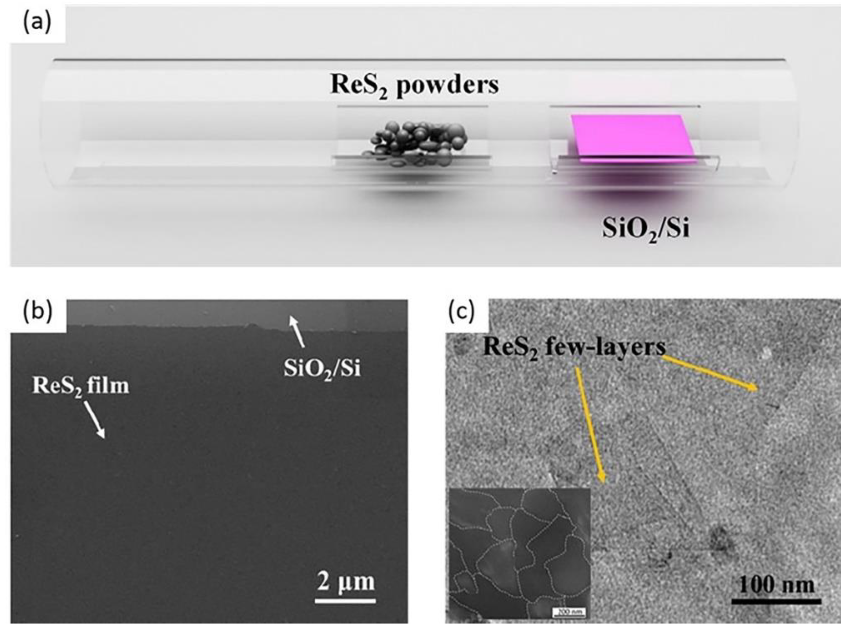
2.2.5. Chemical Vapor Deposition (CVD)

Chemical vapor deposition technique is intensively employed due to high quality, large area and uniform films obtained [100,101]. Large-area monolayer ReS2 thin films are exhibited by Keyshar et al. [102] recently using scalable CVD synthesis method. Remarkably, low temperature (450 °C) growth is reported for monolayer synthesis compared to previous studies. The uniform polycrystalline bilayer ReS2 film is obtained by synthesizing hexagonal single crystal flakes of ReS2 for the first time exploiting CVD method is reported by Hafeez et al. [103]. Three horizontal zones were formed inside the quartz tube within the furnace during the heating process to obtain single and bilayer crystals from the source materials, i.e., ReO3 and sulfur. In another study by Dathbun et al. [104], wafer scale uniform ReS2 multilayer film is prepared using ReO3 and H2S gas as precursor. During the infusion of gas, H2S directly reacted with ReO3 and formed ReS2 film of few cm2. One of the merits of using this technique is the control on obtained film thickness by regulating the gas flow rate. However, this technology involves harmful and complex transfer procedures from the developed substrate to the laser integration platform in order to construct the SA device, making it difficult to create cost-effective devices [105].

3. Photonic Applications

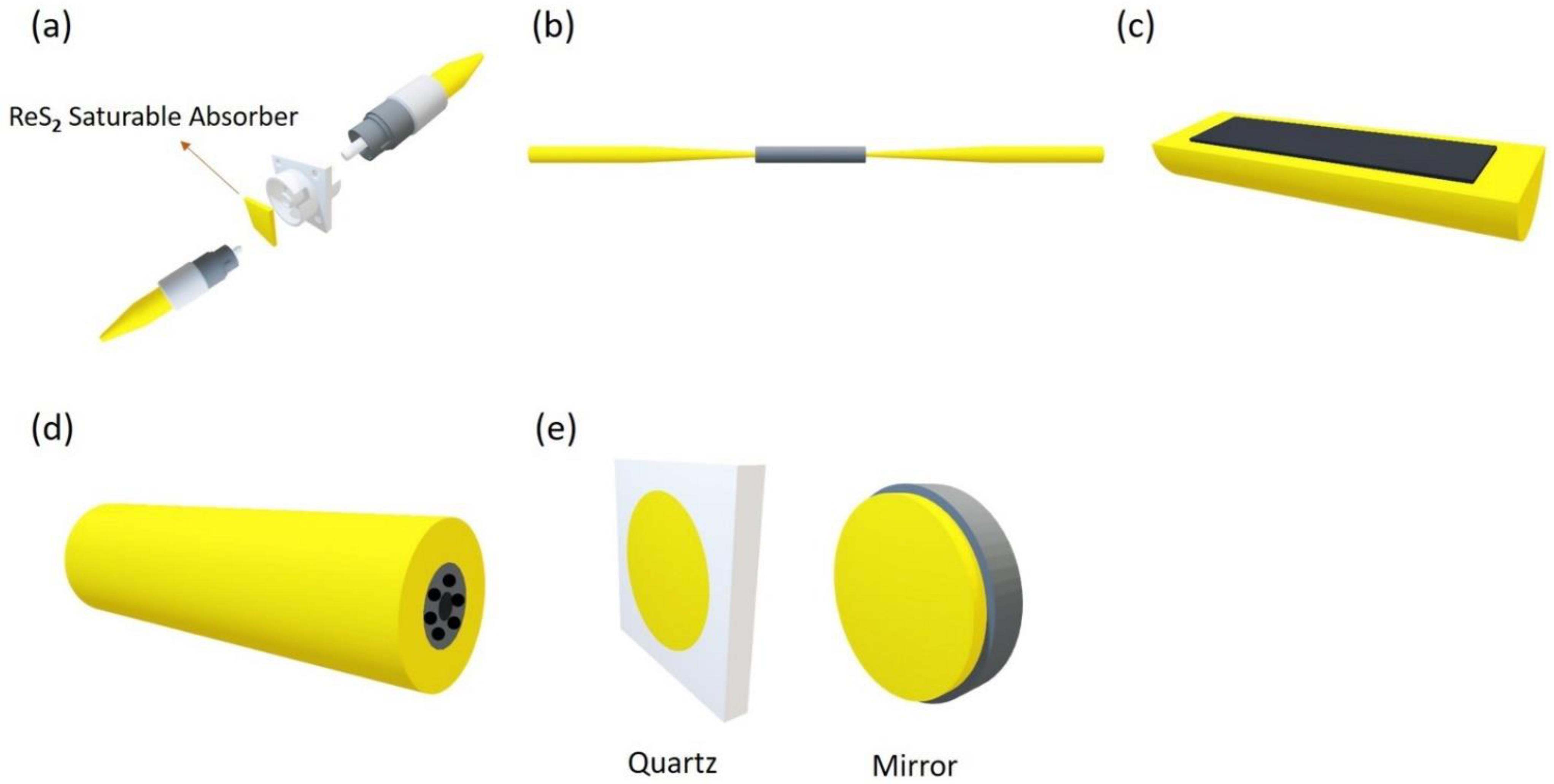
3.1. Saturable Absorbers

The absorption basis of 2D layered materials is primarily the Pauli blocking impact [35,106]; this is schematically depicted in Figure 11. When light having photon energy magnitude more than an incident material’s bandgap falls on the 2D material surface, valence band electrons are excited to the conduction band due to incident photon absorption (Figure 11a). The hot electrons created are swiftly thermalized to institute a hot Fermi–Dirac dissemination. The thermalized carriers are then cooled down more through the intraband scattering impact (Figure 11b). Next, electron-hole recombination process is active until hole distribution is in equilibrium with electron relaxation. Hence, low transmission is the consequence of a majority of incident photons being absorbed. This phenomenon can be attributed for linear optical photon absorption during relatively weak excitation scenario. During high-intensity incident light conditions, there is a substantial increase in photogenerated carriers; consequently, conduction band states are filled with photon energy up to half of their level. This will impede additional absorption due to the Pauli blocking impact (Figure 11c). Pauli blocking effect indicates that two similar electrons cannot occupy an identical state; consequently, light absorption bleaching occurs (majority of the incident light is not absorbed, causing a high transmission) [35].
The produced 2D materials are in the form of thin small sheets having nanometer-scale thickness; hence, they cannot be used directly for lasers. Therefore, it is essential to couple materials into proper optical structures to ease the interface between the light and materials. This type of photonic device having 2D materials utilized in optical fiber or free space structures is known as saturable absorbers (SAs) [58,106]. There are many coupling methods which are summarized in Figure 12. Techniques used for fiber laser applications require material transfer to an end facet of a fiber connector (Figure 12a), tapered fiber (Figure 12b), side-polished fiber (Figure 12c) or filled into the empty photonic crystal fiber (PCF) channels (Figure 12d). It is straightforward and flexible to handle the fiber connector method. A fiber adapter is used to integrate two fibers by placing the SA material in the middle of two end facets. Nevertheless, the obtained material has less damage threshold because SA chemical bonds break due to heat collection due to the high-intensity laser obtained by strong transmission coupling [107]. Side-polished and tapered fiber forms provide the benefit of increased power endurance and damage limits since only a fraction of the light (i.e., evanescent field) interact with the 2D material. Nevertheless, considering that the material has relatively less light intensity, enhancing interaction length can lead to higher non-linearity [108,109]. The PCF scheme is also associated with adequate material-light interaction length and high power-handling ability. In contrast, it is challenging to produce; also, single mode fibers and PCFs have less coupling effectiveness [107]. In the case of solid-state lasers, the coupling schemes are such that there is direct light interaction with the material spin coated on substrates such as mirror or quartz glass surface in free-space using reflection or transmission (Figure 12e).
Choosing an appropriate technique for transferring material onto optical devices relies on material production techniques. Considering the mechanical exfoliation method, it is possible to move flake layers to the fiber connector by pressing down the end facet on scotch tape having few-layer thick peeled flakes. Consequently, the adhesive force between the ceramic and flakes causes a 2D-material layer to deposit on the fiber core (Figure 13a) [41]. Optical-driven deposition may be employed for solution-based exfoliation. Initially, the fiber’s end facet is dipped inside the solution; subsequently, a strong beam of light is injected. Consequently, the fiber tip becomes coated with the material because of temperature-gradient induced material movement [110,111,112], as depicted in Figure 13b. Additionally, solution exfoliation nanomaterials can now be transferred using inkjet printing technology. This technique comprises an ink based on 2D flakes; the ink is deposited on the substrate surface, thereby facilitating precisely controlled production at scale [113,114]. Moreover, these nanomaterials may be spread using polymer films such as PMMA, PVA or other substances. Subsequently, the composite layer is placed in the middle of fiber connectors [115].

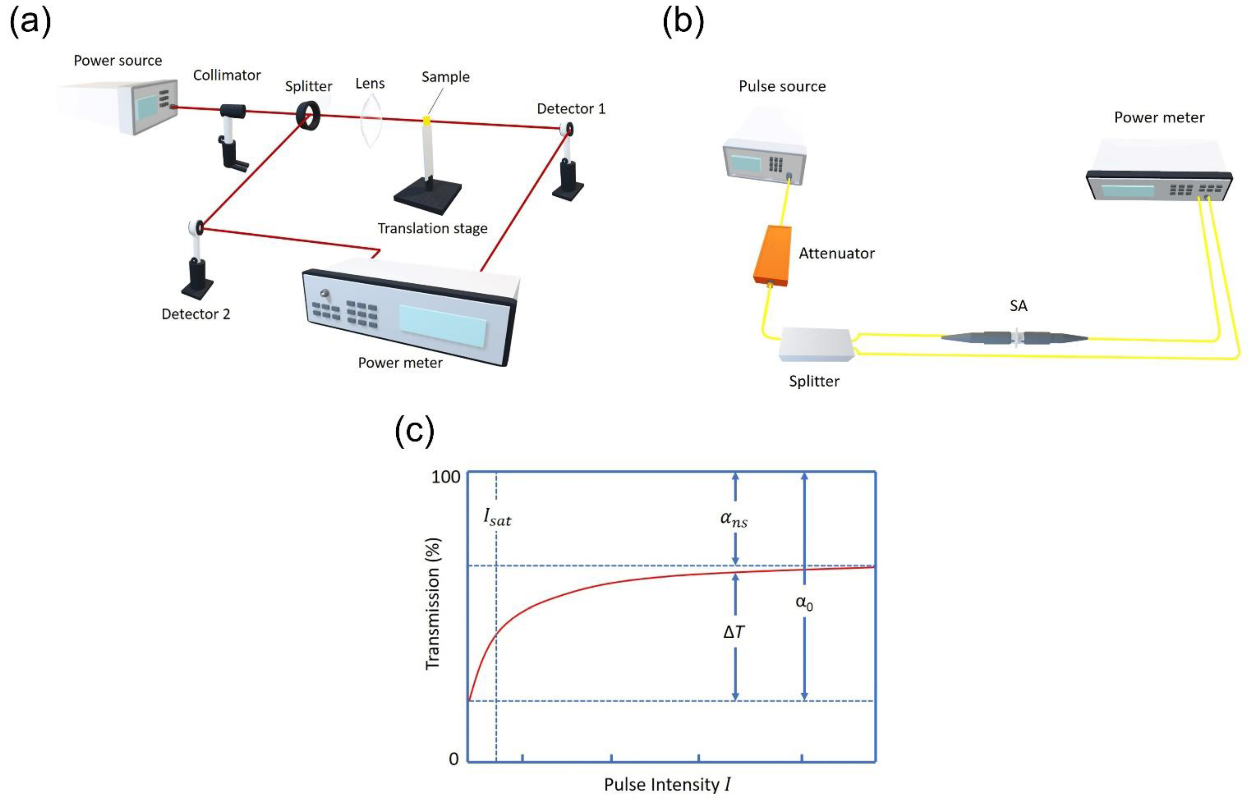
3.2. Nonlinear Absorption Characterization

As per the nonlinear optical theory [116], the expression of the absorption of sample could be acquired based on the relation between the absorption coefficient α and intensity of incident light I as given in Equation (1).
α ( I ) = α 0 +   α NL   I
here, α 0 denotes the linear absorption coefficient and α NL   represents the nonlinear absorption coefficient. The expression of nonlinear absorption of SAs could be acquired as shown in Equation (2) [35,117,118].
α ( I ) = α s 1 + I I sat + α ns
here, α s denotes the saturable loss (also called as modulation depth ΔR or ΔT), I sat signifies the saturation intensity and α ns represents the non-saturable loss. Other key parameters pertaining to SAs include the wavelength range (where it absorbs) as well as recovery time τ A , which need to be of very short time in order to enable passive mode-locking, but not too short with regards to passive Q-switching [119].
For convenience, expression of I can be acquired as the energy E as well as the incident light’s fluence F, thus I sat in Equation (2) could be replaced by the saturation energy E sat as well as saturation fluence F sat [120]. Various SA parameters with their units and definitions are summarized in Table 1 below:
Two common measurement techniques can be employed to characterize these SA parameters: I-scan measurement (often called as the balanced twin-detector technique) [121] and Z-scan measurement [116,122]. The Z-scan measurement technique allows characterizing the free-space-type SA sample. As presented in Figure 14a, with the help of a splitter, the pulsed light is first split into two beams of light from the pumping source. The measurement beam would be the beam that propagates along the SA sample’s incorporated path, while the other beam would be regarded as the reference beam. The measurement beam is focused by a lens to the SA sample, which has been mounted on a Z-direction translation stage. Changing of light intensity per unit area of the sample can be acquired based on various beam sizes by moving the sample towards the z-axis along with the measurement beam. The dual-channel power meter is employed to collect the power from both paths. The power from the two detectors is compared in order to obtain the sample’s nonlinear absorption. Closed-aperture Z-scan measurement may explore the Kerr effect of the sample and acquire the nonlinear index because the beam diameter after the sample is connected to the beam induced refractive index change of the sample [116]. Balanced twin-detector measurement is chosen for SAs that have been integrated as the fiber-based device to perform nonlinear absorption characterization. The principle can be said to be analogous to Z-scan, except that the setup is completely fiberized (Figure 14b). An optical coupler is employed to split the light from a pulsed laser into reference and measurement beams. In contrast with the Z-scan method, a variable optical attenuator is mounted before the optical coupler in order to achieve the variation in light intensity for twin-detector measurement [58].
The optical attenuator is employed to change the input power gradually, which enables recording a series of optical transmittance based on different input intensities. Then, characterization and plotting (Figure 14c) of the corresponding nonlinear optical parameters can be acquired via fitting the relation between the input laser power (I) and the optical transmission rate T ( I ) based on Equation (3) [108].
T ( I ) = 1 Δ T exp ( I / I sat )   α ns
Based on the operation of Q-switching or mode-locking, integrating SA devices within the laser cavity can aid in creating short optical pulses. Usually, Q-switching can generate pulses possessing high energy (μJ–mJ) at low repetition frequency (kHz) as well as pulse durations in the range of μs–ns. While shorter durations (ps–fs) at higher repetition rate (MHz–GHz) are associated with the mode-locked laser pulses, they also possess lower energy versus Q-switched lasers (pJ–μJ). Both mode-locking and Q-switching can exist together within the same laser cavity but with differing thresholds. Various factors such as gain and loss in cavity due to alteration of input power, and balancing between cavity’s dispersion and nonlinearity [114] can impact the transition between the two operations.

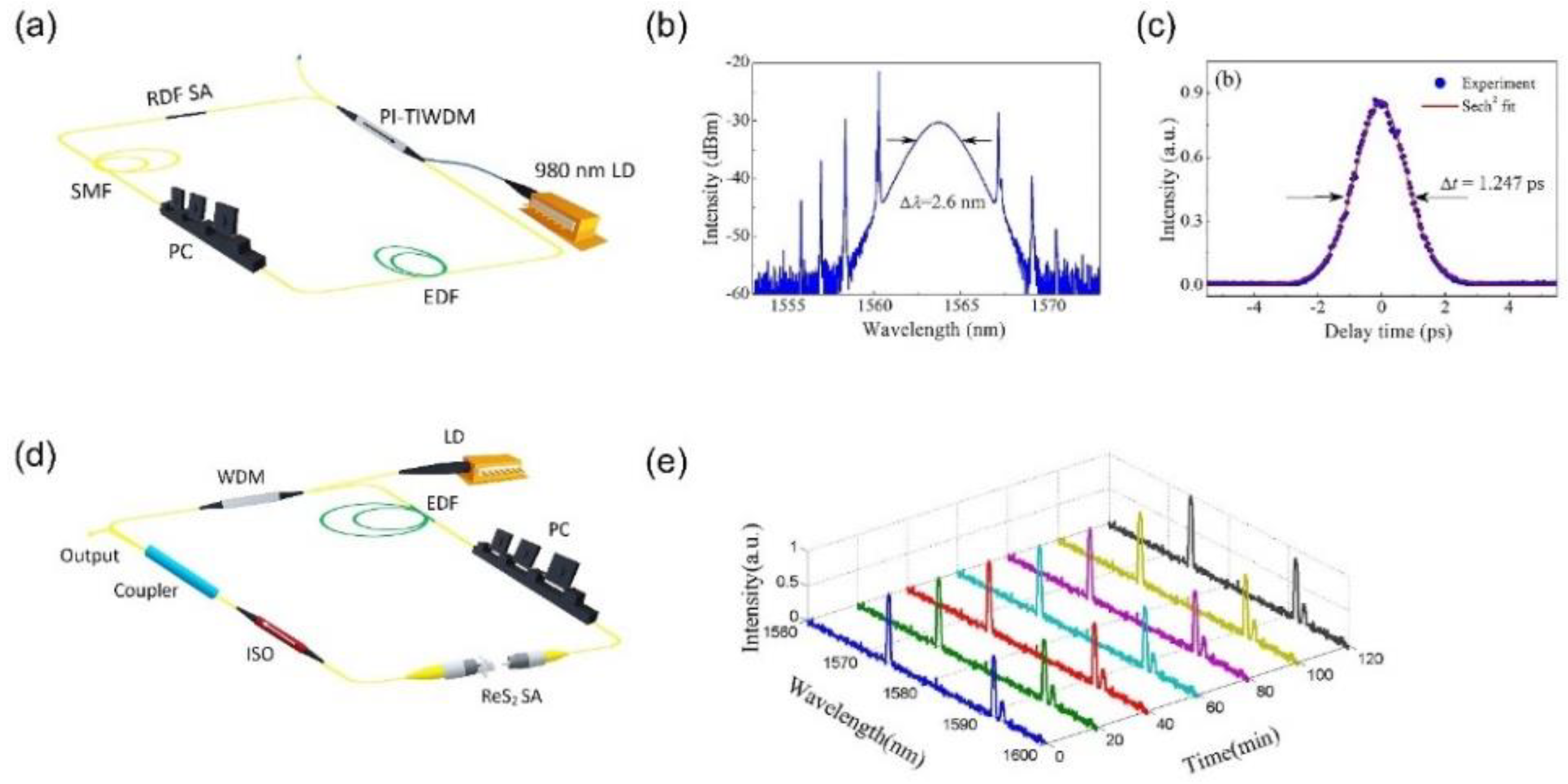
3.3. Q-Switched Lasers

Typically, Q-switching operation gives pulses possessing higher energy as well as peak power versus mode-locked lasers. Table 2 presents the performance pertaining to Q-switched fiber lasers as well as solid-state lasers with regards to ReS2-SA. X. Su et al. presented the initial work [62], in which they showed a Q-switched Er:YSGG solid-state pulsed laser at 2.8 μm along with 324 ns pulse duration. Later, various bulk gain medium such as Er:SrF2, Pr:YLF, Nd:GdLaNbO4, Tm:YAP and Nd:YAG, were employed, which encompassed broad wavelengths ranging from 640 nm to 2950 nm [68,123]. The ReS2 was spin-coated on various substrates such as mirror, quartz, sapphire, Yttrium, aluminum garnet (YAG) and K9 glass in order to fabricate the SA device [71,124,125].
With regards to fiber-based laser system, Xu et al. and B. Lu et al. employed Erbium and Ytterbium-doped fibers in order to produce Q-switched laser pulses at 1 μm and 1.5 μm waveband with an average output power of 2.48 mW and 3.2 mW [61,126], respectively. In contrast to fiber lasers, solid-state pulsed lasers offer the benefits of low undesirable nonlinear impacts as well as a wider mode area, which make them optimum for applications that need high power sources [35]. Q-switched solid-state laser possessing maximum average output power of 580 mW as well as highest peak power of 22.1 W was reported by M. Fan et al. who employed Er:SrF2 crystal as gain medium [125].
Apart from the wide application in infrared lasers, ReS2-SA is employed for the visible spectrum region. X. Su et al. designed a passively Q-switched laser at 640 nm, which possessed 160 ns pulse duration and 52 mW average output power [123]. Moreover, a Q-switched Nd-doped crystal laser was reported by Han et al. close to ReS2 bandgap at 950 nm [71]. Various schematic setups are demonstrated in Figure 15 in order to generate Q-switched lasers based on ReS2-SA as well as their output characteristics at 1047 nm, 1064 nm and 1557.3 nm [63,69,126].

3.4. Mode-Locked Lasers

The performance of mode-locked lasers based on ReS2 SA is shown in Table 3. As observed, majority of the reports were found to be on near-infrared communication band at 1.5 μm by employing Erbium fiber as gain medium. High quality beam can be produced via fiber lasers platforms along with alignment-free, compact and low-cost structure [30]. In 2017, first identification of mode-locking operation that was based on ReS2-SA was acquired [60]. By including the D-shaped fiber possessing ReS2–polymer composite, generation of mode-locked pulses centered at 1564 nm with pulse duration of 1.25 ps was acquired as demonstrated in Figure 16a–c. In addition, stable mode-locked pulses at 1563.3 nm possessing pulse width of 3.8 ps was reported by Xu et al. The nature of double covered ReS2 microfiber structure allowed obtaining high optical damage threshold of 410 mw [67]. In addition, a multi-wavelength Er-doped fiber laser (1573.5 nm, 1591.1 nm and 1592.6 nm) was produced by sandwiching ReS2 between the two fiber connecters as presented in Figure 16d [65]. Figure 16e displays the output spectrum, which was monitored for about 2 h to observe long-term stability operation. Similarly, Mao et al. employed a fiber connecter to build a ReS2-SA device inside the Erbium-doped fiber laser (EDFL) system, which allowed obtaining self-started mode-locked pulses that were centered at 1558.6 nm along with the duration of 1.6 ps by altering the polarization controller [63]. The first report was realized with regarding mode-locked laser employing ReS2 in longer wavelengths at 2 μm waveband in thulium-doped fiber laser possessing 893 fs pulse duration as well as 4.13 mw maximum average power [128]. Su et al. employed Yb:CALGO solid-state laser as well as ReS2 saturable absorption mirror (SAM) to produce 1060 nm mode-locked laser pulses with higher average output power of 350 mW as well as shorter pulse duration of 323 fs [123]. These reports demonstrate that ReS2 can be employed as broadband SA for various wavelengths, at discrete or multiwavelength operation.
Apart from the broadband saturable absorption, we can also employ large third-order nonlinear effects of ReS2 to yield pulses possessing high repetition rates with potential applications in frequency combs and soliton communications. Feifei Lu produced pulses with repetition rate, which could reach as high as 318.5 MHz and corresponded to the 168th harmonic mode-locking of Erbium-doped fiber laser [17].

4. Discussion and Outlook

As for the reported results on employing ReS2 as saturable absorber, the laser performance showed steady improvements. With regards to integration, variety of transfer methods were utilized, such as embedding ReS2 within polymer composite [64], optical driven deposition [65], spin coating [123] and drop casting [69]. Material fabrication techniques exhibited consistent progress in being more controllable such as CVD [127] and low-cost fabrication such as mechanical exfoliation [126]. As depicted in Figure 17, the operation bands of ReS2-based SA have been employed successfully for various wavelength regions ranging from visible to mid-infrared (0.64–3 μm) in fiber-based as well as solid state laser systems [61,68,71,123,128] leading to several optical applications.
The bandgap of ReS2 amounts to ~1.4 eV which corresponds to an optical absorption at ~800 nm wavelength [130]. Nonetheless, previous works have reported generation of Q-switched and mode-locked lasers using ReS2 functioning as SA at 1550 nm (~0.8 eV) and 2950 nm (~0.4 eV), which is much less than the bandgap of ReS2. Thus, in theory, there ought to be no light absorption. Nonetheless, the absorption occurs due to the unavoidable deficiencies in the formation of the material, e.g., grain boundaries and point defects [60]. The introduction of crystallographic or the edge state defect in the material enables the absorption of light photons with energies less than the material bandgap (i.e., sub-bandgap absorption) [131]. By leveraging the effect of sub-bandgap absorption, ReS2 based SA could consequently support pulsed lasers in the mid-infrared and near-infrared wavelengths where energies of the photons are less than the intended material bandgap. Various theories have been developed to rationalize the sub-bandgap absorption of TMDs, namely decrease in bandgap due to defects [132,133], materials’ edge state [134] (can be considered as a special defect at the nanosheets’ edges) and saturation of two-photon absorption [135]. X. Su et al. computed the ReS2 band structure with various ratios of Re and S by using technique of Vienna ab initio simulation, and the results suggest that the bandgap can be decreased from 1.38 to 0.56 eV by introducing S defects in an appropriate range [123]. Moreover, Horzum et al. theoretically examined the atomic imperfections in monolayer ReS2. It was observed that the S vacancy formation decreases the bandgap from 1.43 to 1.08 eV and the bandgap with Re imperfections becomes only 0.35 eV [136].
The modulation depth, as the main classification parameter of the nonlinear absorption of SA, which is significantly influenced by the material thickness, has a considerable impact on the laser performance. Considerable modulation depth is advantageous for producing short pulses. A concern for monolayer ReS2-SA (thickness of 0.7 nm [54]) is the low modulation depth that is generally 1% only [60]. By increasing the ReS2 thickness, the modulation depth can be increased. B. Lu et al. attained up to 44% modulation depth by piling up 30 layers (21 nm) of ReS2 [126], though this also increases the thresholds of saturation intensity. This is due to the fact that thicker films have higher density of localized defective states on the grain edge and more photons are trapped [67,137]. Intensity/fluence of high saturation implies that the pulsed function can be initiated at higher power level.
Nonetheless, increasing the thickness may have a reverse or positive impact on modulation depth [107]. Mao et al. obtained only 0.12% modulation depth with 6 layers (4 nm) of ReS2 [63]. ReS2-SA performance also depends on the wavelength of operation. X. Su et al. demonstrates a reduction in the saturation fluence at higher wavelengths, for instance, 58.2 μJ/ cm 2 at 640 nm, 21.5 μJ/ cm 2 at 1064 nm and 2.7 μJ/ cm 2 at 1991 nm [123]. This dependence on wavelength makes the use of ReS2-SA in the mid-infrared region more favorable.
Saturable absorbers having low optical damage threshold can lead to collapse of pulsed operation and instead of that, the laser engages in CW operation, particularly when the material becomes deposited on the fiber connector’s tip, where the laser connects directly with the material. For instance, pump power above 330 mW caused strong signal jittering to dominate and obliterate the Q-switched pulses [61]; nonetheless, the Q-switched pulses could be obtained again just by reducing the pump power. This is because of the over-saturation of ReS2-SA instead of thermal damage [138,139]. Many attempts have been carried out to increase the ReS2-SA damage threshold by utilizing the evanescent field effect through D-shaped or tapered fibers. X. Xu et al. attained stable mode-locking pulses with comparatively high laser damage threshold of 410 mW through double covered ReS2 micro-fiber as SA device [67].
One of the challenges lies in a proper deposition/transferring process of the material into the laser system. If the material is not distributed entirely and evenly on the laser integration platform, only a fraction of the region of ReS2 can sustain the Q-switching/mod-locking operation which may cause deterioration in long-term stability performance. Moreover, ReS2 production is costly due to its complex structure and low abundance on earth [140]. Furthermore, generating finely tunable pulsed laser with high performance based on ReS2-SA is still difficult. Using ultrafast laser in the mid-infrared region can advance the chemical and biomedical sensing applications, since many absorption bands of molecular solids, liquids and gases can be found in this particular region [141]. However, only one study has reported ultrafast sub-picosecond mode-locked pulses in the MIR region using ReS2-SA [128].
A future direction for the SAs is to investigate the integration of the emergent ReS2 with conventional well-established materials such as MoS2 and WS2 to form heterostructures [142,143,144,145]. This is likely to help in achieving SAs with greater nonlinearity, higher damage threshold, as well as ultrafast relaxation time by using the properties of various materials. Furthermore, developing hybrid SAs by using artificial SAs such as NPE, and real SAs can increase the parameter modulation depth and improve the performance of the output laser. Several applications will be benefited from such ultrafast lasers, and we suppose ReS2 is a potential material for SAs devices based on different laser sources.
Finally, we note that ReS2 is only one member of the TMDs family which has unique and strong anisotropic properties. We believe that further study on these properties can stimulate the use of other similar low symmetry 2D materials in developing innovative photonic devices.

5. Conclusions

In this review, we have emphasized how the property of broadband absorption and large third-order nonlinear effect of ReS2 can help in the development of flexible and low-cost SAs integrated in fiber-based and solid-state lasers. The ReS2-SA has been effectively used in short pulse generation, providing pulses with maximum peak power up to 22 W, broadband wavelength extending from visible (640 nm) to mid-infrared (2.95 μm) range, and pulse widths down to as low as 270 fs. Moreover, high signal-to-noise ratio (SNR) of more than 70 dB was observed, which demonstrates the high level of pulse stability. These outcomes show that ReS2 is a potential material for several applications such as broadband optical modulator, pulsed lasers and sensors. Majority of the studies utilized liquid-phase exfoliation to form ReS2. Liquid-phase exfoliation technique is an efficient, convenient and cheap method to produce 2D materials. Molecular beam epitaxy (MBE) is another interesting fabrication method which has not been employed yet for ReS2 synthesis. MBE is regarded as one of the most effective techniques for controlling the number of layers while maintaining monolayer homogeneity. This review produces an introduction to the potential of ReS2 as novel saturable absorber for ultrafast photonic technology. Nonetheless, the most challenging concern is to use these controlled laboratory photonic devices in environmentally stable industrial applications.

Author Contributions

M.M.F. drafted the original manuscript, data collection, data analysis and conceptualization; N.A. (Norazida Ali) further data collection; H.R., methodology; N.A. (Norhana Arsad) supervised and validated the work with the help of other authors of N.M.S., A.E.H., M.S.D.Z., N.A.A. All authors have read and agreed to the published version of the manuscript.

Funding

Kementerian Sains, Teknologi dan Inovasi (MOSTI) with grant code IF0419IF1082 and Universiti Kebangsaan Malaysia under Modal Insan funding with grant code MI-2020-002 and GUP-2019-010.

Acknowledgments

The authors gratefully acknowledge the financial support of the Department of Electrical, Electronic and Systems Engineering/Faculty of Engineering and Built Environment/Universiti Kebangsaan Malaysia (UKM) for their encouragement and grant support (MI-2020-002, GUP-2019-010 and IF0419IF1082).

Conflicts of Interest

The authors declare no conflict of interest.

References

  1. Keller, U. Recent developments in compact ultrafast lasers. Nature 2003, 424, 831–838. [Google Scholar] [CrossRef] [PubMed]
  2. Shi, W.; Fang, Q.; Zhu, X.; Norwood, R.A.; Peyghambarian, N. Fiber lasers and their applications. Appl. Opt. 2014, 53, 6554–6568. [Google Scholar] [CrossRef] [PubMed]
  3. Kobayashi, T. Development of ultrashort pulse lasers for ultrafast spectroscopy. Photonics 2018, 5, 19. [Google Scholar] [CrossRef] [Green Version]
  4. Morgenweg, J.; Barmes, I.; Eikema, K.S.E. Ramsey-comb spectroscopy with intense ultrashort laser pulses. Nat. Phys. 2014, 10, 30–33. [Google Scholar] [CrossRef] [Green Version]
  5. Udem, T.; Holzwarth, R.; Hänsch, T.W. Optical frequency metrology. Nature 2002, 416, 233–237. [Google Scholar] [CrossRef]
  6. Muhanad Fadhel, M.; Rashid, H.; Essa Hamzah, A.; Dzulkefly Zan, M.S.; Abd Aziz, N.; Arsad, N. Flat frequency comb generation employing cascaded single-drive Mach–Zehnder modulators with a simple analogue driving signal. J. Mod. Opt. 2021, 68, 536–541. [Google Scholar] [CrossRef]
  7. Elgaud, M.M.; Bakar, A.A.A.; Ghaith, A.A.; Naim, N.F.; Arsad, N.; Mokhtar, M.H.H.; Azeman, N.H.; Zan, M.S.D. Pulse Compressed Time Domain Multiplexed Fiber Bragg Grating Sensor: A Comparative Study. IEEE Access 2018, 6, 64427–64434. [Google Scholar] [CrossRef]
  8. Hamzah, A.E.; Zan, M.S.D.; Elgaud, M.; Fadhel, M.M.; Alwash, S.A.; Abushagur, A.A.; Mokhtar, M.H.H.; Azeman, N.H.; Ali, S.H.b.M.; Bakar, A.A.A. Signal Generation using System on Chip for Coded Fiber Bragg Grating Sensor. In Proceedings of the 2020 IEEE 8th International Conference on Photonics (ICP), Kota Bharu, Malaysia, 12 May–30 June 2020; pp. 80–81. [Google Scholar]
  9. Zan, M.S.D.; Elgaud, M.M.; Zainuddin, A.R.; Kadhim, A.S.; Mokhtar, M.H.H.; Arsad, N.; Bakar, A.A.A. Simulation Analysis on the Simultaneous Deployment of Brillouin Gain and Loss in Coded Brillouin Optical Time Domain Analysis (BOTDA) Fiber Sensor. J. Phys. Conf. Ser. 2021, 1892, 012034. [Google Scholar] [CrossRef]
  10. Liu, X.; Cui, Y.; Han, D.; Yao, X.; Sun, Z. Distributed ultrafast fibre laser. Sci. Rep. 2015, 5, 9101. [Google Scholar] [CrossRef] [PubMed] [Green Version]
  11. Taha, B.A.; Ali, N.; Sapiee, N.M.; Fadhel, M.M.; Mat Yeh, R.M.; Bachok, N.N.; Al Mashhadany, Y.; Arsad, N. Comprehensive Review Tapered Optical Fiber Configurations for Sensing Application: Trend and Challenges. Biosensors 2021, 11, 253. [Google Scholar] [CrossRef]
  12. Ippen, E.P. Principles of passive mode locking. Appl. Phys. B 1994, 58, 159–170. [Google Scholar] [CrossRef]
  13. Liu, J.; Wu, J.; Chen, H.; Chen, Y.; Wang, Z.; Ma, C.; Zhang, H. Short-pulsed Raman fiber laser and its dynamics. Sci. China Phys. Mech. 2020, 64, 214201. [Google Scholar] [CrossRef]
  14. Haus, H.A. Mode-locking of lasers. IEEE J. Sel. Top. Quantum Electron. 2000, 6, 1173–1185. [Google Scholar] [CrossRef]
  15. Xia, W.; Chen, X. Recent developments in fiber-based optical frequency comb and its applications. Meas. Sci. Technol. 2016, 27, 041001. [Google Scholar] [CrossRef] [Green Version]
  16. Woodward, R.I.; Kelleher, E.J. 2D saturable absorbers for fibre lasers. Appl. Sci. 2015, 5, 1440–1456. [Google Scholar] [CrossRef] [Green Version]
  17. Lu, F. Passively harmonic mode-locked fiber laser based on ReS2 saturable absorber. Mod. Phys. Lett. B 2017, 31, 1750206. [Google Scholar] [CrossRef]
  18. Soffer, B.H. Giant Pulse Laser Operation by a Passive, Reversibly Bleachable Absorber. J. Appl. Phys. 1964, 35, 2551. [Google Scholar] [CrossRef]
  19. Bret, G.; Gires, F. Giant-Pulse Laser and Light Amplifier Using Variable Transmission Coefficient Glasses as Light Switches. Appl. Phys. Lett. 1964, 4, 175–176. [Google Scholar] [CrossRef]
  20. Maiman, T.H. Stimulated Optical Radiation in Ruby. Nature 1960, 187, 493–494. [Google Scholar] [CrossRef]
  21. Ippen, E.P.; Shank, C.V.; Dienes, A. Passive mode locking of the cw dye laser. Appl. Phys. Lett. 1972, 21, 348–350. [Google Scholar] [CrossRef]
  22. Dzhibladze, M.I.; Ésiashvili, Z.G.; Teplitskiĭ, É.S.; Isaev, S.K.; Sagaradze, V.R. Mode locking in a fiber laser. Sov. J. Quantum Electron. 1983, 13, 245–247. [Google Scholar] [CrossRef]
  23. Keller, U.; Miller, D.; Boyd, G.; Chiu, T.; Ferguson, J.; Asom, M. Solid-state low-loss intracavity saturable absorber for Nd: YLF lasers: An antiresonant semiconductor Fabry–Perot saturable absorber. Opt. Lett. 1992, 17, 505–507. [Google Scholar] [CrossRef]
  24. Bogusławski, J.; Wang, Y.; Xue, H.; Yang, X.; Mao, D.; Gan, X.; Ren, Z.; Zhao, J.; Dai, Q.; Soboń, G.; et al. Graphene Actively Mode-Locked Lasers. Adv. Funct. Mater. 2018, 28, 1801539. [Google Scholar] [CrossRef]
  25. Wen, Q.-Y.; Tian, W.; Mao, Q.; Chen, Z.; Liu, W.-W.; Yang, Q.-H.; Sanderson, M.; Zhang, H.-W. Graphene based All-Optical Spatial Terahertz Modulator. Sci. Rep. 2014, 4, 7409. [Google Scholar] [CrossRef] [PubMed]
  26. Zhang, H.; Healy, N.; Shen, L.; Huang, C.C.; Hewak, D.W.; Peacock, A.C. Enhanced all-optical modulation in a graphene-coated fibre with low insertion loss. Sci. Rep. 2016, 6, 23512. [Google Scholar] [CrossRef] [Green Version]
  27. Cho, B.; Hahm, M.G.; Choi, M.; Yoon, J.; Kim, A.R.; Lee, Y.-J.; Park, S.-G.; Kwon, J.-D.; Kim, C.S.; Song, M.; et al. Charge-transfer-based Gas Sensing Using Atomic-layer MoS2. Sci. Rep. 2015, 5, 8052. [Google Scholar] [CrossRef]
  28. Wang, S.; Wang, J.; Zhao, W.; Giustiniano, F.; Chu, L.; Verzhbitskiy, I.; Zhou Yong, J.; Eda, G. Efficient Carrier-to-Exciton Conversion in Field Emission Tunnel Diodes Based on MIS-Type van der Waals Heterostack. Nano Lett. 2017, 17, 5156–5162. [Google Scholar] [CrossRef]
  29. Sun, X.; Qiu, C.; Wu, J.; Zhou, H.; Pan, T.; Mao, J.; Yin, X.; Liu, R.; Gao, W.; Fang, Z.; et al. Broadband photodetection in a microfiber-graphene device. Opt. Express 2015, 23, 25209–25216. [Google Scholar] [CrossRef] [PubMed]
  30. Martinez, A.; Sun, Z. Nanotube and graphene saturable absorbers for fibre lasers. Nat. Photonics 2013, 7, 842–845. [Google Scholar] [CrossRef]
  31. Hu, X.; Yasaei, P.; Jokisaari, J.; Öğüt, S.; Salehi-Khojin, A.; Klie, R.F. Mapping thermal expansion coefficients in freestanding 2D materials at the nanometer scale. Phys. Rev. Lett. 2018, 120, 055902. [Google Scholar] [CrossRef] [PubMed] [Green Version]
  32. Guerreiro, P.T.; Ten, S.; Borrelli, N.F.; Butty, J.; Jabbour, G.E.; Peyghambarian, N. PbS quantum-dot doped glasses as saturable absorbers for mode locking of a Cr:forsterite laser. Appl. Phys. Lett. 1997, 71, 1595–1597. [Google Scholar] [CrossRef]
  33. Set, S.Y.; Yaguchi, H.; Tanaka, Y.; Jablonski, M. Ultrafast fiber pulsed lasers incorporating carbon nanotubes. IEEE J. Sel. Top. Quantum Electron. 2004, 10, 137–146. [Google Scholar] [CrossRef]
  34. Bao, Q.; Zhang, H.; Wang, Y.; Ni, Z.; Yan, Y.; Shen, Z.X.; Loh, K.P.; Tang, D.Y. Atomic-layer graphene as a saturable absorber for ultrafast pulsed lasers. Adv. Funct. Mater. 2009, 19, 3077–3083. [Google Scholar] [CrossRef]
  35. Zhang, B.; Liu, J.; Wang, C.; Yang, K.; Lee, C.; Zhang, H.; He, J. Recent Progress in 2D Material-Based Saturable Absorbers for All Solid-State Pulsed Bulk Lasers. Laser Photonics Rev. 2020, 14, 1900240. [Google Scholar] [CrossRef]
  36. Novoselov, K.S.; Geim, A.K.; Morozov, S.V.; Jiang, D.; Zhang, Y.; Dubonos, S.V.; Grigorieva, I.V.; Firsov, A.A. Electric field effect in atomically thin carbon films. Science 2004, 306, 666–669. [Google Scholar] [CrossRef] [PubMed] [Green Version]
  37. Zhao, C.; Zhang, H.; Qi, X.; Chen, Y.; Wang, Z.; Wen, S.; Tang, D. Ultra-short pulse generation by a topological insulator based saturable absorber. Appl. Phys. Lett. 2012, 101, 211106. [Google Scholar] [CrossRef]
  38. Salim, M.A.M.; Ab Razak, M.Z.; Azzuhri, S.R.; Ismail, M.A. Generation of Microsecond Ytterbium-Doped Fibre Laser Pulses using Bismuth Telluride Thin Film as Saturable Absorber. Sains Malays. 2019, 48, 1289–1294. [Google Scholar] [CrossRef]
  39. Zhang, H.; Lu, S.; Zheng, J.; Du, J.; Wen, S.; Tang, D.; Loh, K. Molybdenum disulfide (MoS2) as a broadband saturable absorber for ultra-fast photonics. Opt. Express 2014, 22, 7249–7260. [Google Scholar] [CrossRef]
  40. Aizi Mat Salim, M.; Razalli Azzuhri, S.; Afiq Ismail, M.; Ab Razak, M.Z. Few Layer Molybdenum Selenide Saturable Absorber using Optical Deposition Technique for Q-switched Ytterbium Pulses Laser Generation. J. Phys. Conf. Ser. 2020, 1484, 012025. [Google Scholar] [CrossRef]
  41. Chen, Y.; Jiang, G.; Chen, S.; Guo, Z.; Yu, X.; Zhao, C.; Zhang, H.; Bao, Q.; Wen, S.; Tang, D. Mechanically exfoliated black phosphorus as a new saturable absorber for both Q-switching and mode-locking laser operation. Opt. Express 2015, 23, 12823–12833. [Google Scholar] [CrossRef] [Green Version]
  42. Sotor, J.; Sobon, G.; Macherzynski, W.; Paletko, P.; Abramski, K.M. Black phosphorus saturable absorber for ultrashort pulse generation. Appl. Phys. Lett. 2015, 107, 051108. [Google Scholar] [CrossRef] [Green Version]
  43. Jhon, Y.I.; Koo, J.; Anasori, B.; Seo, M.; Lee, J.H.; Gogotsi, Y.; Jhon, Y.M. Metallic MXene saturable absorber for femtosecond mode-locked lasers. Adv. Mater. 2017, 29, 1702496. [Google Scholar] [CrossRef] [PubMed]
  44. Song, Y.; Liang, Z.; Jiang, X.; Chen, Y.; Li, Z.; Lu, L.; Ge, Y.; Wang, K.; Zheng, J.; Lu, S.; et al. Few-layer antimonene decorated microfiber: Ultra-short pulse generation and all-optical thresholding with enhanced long term stability. 2D Mater. 2017, 4, 045010. [Google Scholar] [CrossRef]
  45. Hu, P.; Liu, Y.; Guo, L.; Ge, X.; Liu, X.; Yu, L.; Liu, Q. Passively Q-switched erbium-doped fiber laser based on antimonene as saturable absorber. Appl. Opt. 2019, 58, 7845–7850. [Google Scholar] [CrossRef]
  46. Lu, L.; Liang, Z.; Wu, L.; Chen, Y.; Song, Y.; Dhanabalan, S.C.; Ponraj, J.S.; Dong, B.; Xiang, Y.; Xing, F.; et al. Few-layer Bismuthene: Sonochemical Exfoliation, Nonlinear Optics and Applications for Ultrafast Photonics with Enhanced Stability. Laser Photonics Rev. 2018, 12, 1700221. [Google Scholar] [CrossRef]
  47. Chai, T.; Li, X.; Feng, T.; Guo, P.; Song, Y.; Chen, Y.; Zhang, H. Few-layer bismuthene for ultrashort pulse generation in a dissipative system based on an evanescent field. Nanoscale 2018, 10, 17617–17622. [Google Scholar] [CrossRef]
  48. Guo, B.; Wang, S.-H.; Wu, Z.-X.; Wang, Z.-X.; Wang, D.-H.; Huang, H.; Zhang, F.; Ge, Y.-Q.; Zhang, H. Sub-200 fs soliton mode-locked fiber laser based on bismuthene saturable absorber. Opt. Express 2018, 26, 22750–22760. [Google Scholar] [CrossRef]
  49. Ma, X.; Zhang, Z.; Jiang, W.; Tong, L.; Liu, S.; Dai, W.; Chen, W.; Zhou, Y.; Zhang, W.; Qiu, J.; et al. Passively mode-locked thulium doped fiber laser based on SnSe nanoparticles as a saturable absorber. Opt. Laser Technol. 2021, 138, 106870. [Google Scholar] [CrossRef]
  50. Chhowalla, M.; Shin, H.S.; Eda, G.; Li, L.-J.; Loh, K.P.; Zhang, H. The chemistry of two-dimensional layered transition metal dichalcogenide nanosheets. Nat. Chem. 2013, 5, 263–275. [Google Scholar] [CrossRef]
  51. Wilson, J.A.; Yoffe, A. The transition metal dichalcogenides discussion and interpretation of the observed optical, electrical and structural properties. Adv. Phys. 1969, 18, 193–335. [Google Scholar] [CrossRef]
  52. Li, X.; Chen, C.; Yang, Y.; Lei, Z.; Xu, H. 2D Re-Based Transition Metal Chalcogenides: Progress, Challenges, and Opportunities. Adv. Sci. 2020, 7, 2002320. [Google Scholar] [CrossRef]
  53. Rahman, M.; Davey, K.; Qiao, S.Z. Advent of 2D rhenium disulfide (ReS2): Fundamentals to applications. Adv. Funct. Mater. 2017, 27, 1606129. [Google Scholar] [CrossRef] [Green Version]
  54. Tongay, S.; Sahin, H.; Ko, C.; Luce, A.; Fan, W.; Liu, K.; Zhou, J.; Huang, Y.-S.; Ho, C.-H.; Yan, J.; et al. Monolayer behaviour in bulk ReS2 due to electronic and vibrational decoupling. Nat. Commun. 2014, 5, 3252. [Google Scholar] [CrossRef] [PubMed] [Green Version]
  55. Zhang, Q.; Fu, L. Novel Insights and Perspectives into Weakly Coupled ReS2 toward Emerging Applications. Chem 2019, 5, 505–525. [Google Scholar] [CrossRef] [Green Version]
  56. Zhang, E.; Jin, Y.; Yuan, X.; Wang, W.; Zhang, C.; Tang, L.; Liu, S.; Zhou, P.; Hu, W.; Xiu, F. ReS2-Based Field-Effect Transistors and Photodetectors. Adv. Funct. Mater. 2015, 25, 4076–4082. [Google Scholar] [CrossRef] [Green Version]
  57. Zulkefli, A.; Mukherjee, B.; Iwasaki, T.; Hayakawa, R.; Nakaharai, S.; Wakayama, Y. Gate-bias tunable humidity sensors based on rhenium disulfide field-effect transistors. Jpn. J. Appl. Phys. 2020, 60, SBBH01. [Google Scholar] [CrossRef]
  58. Hao, Q.; Wang, C.; Liu, W.; Liu, X.; Liu, J.; Zhang, H. Low-dimensional saturable absorbers for ultrafast photonics in solid-state bulk lasers: Status and prospects. Nanophotonics 2020, 9, 2603–2639. [Google Scholar] [CrossRef]
  59. Liu, X.; Gao, Q.; Zheng, Y.; Mao, D.; Zhao, J. Recent progress of pulsed fiber lasers based on transition-metal dichalcogenides and black phosphorus saturable absorbers. Nanophotonics 2020, 9, 2215–2231. [Google Scholar] [CrossRef] [Green Version]
  60. Cui, Y.; Lu, F.; Liu, X. Nonlinear Saturable and Polarization-induced Absorption of Rhenium Disulfide. Sci. Rep. 2017, 7, 40080. [Google Scholar] [CrossRef] [PubMed]
  61. Xu, X.; Jiang, M.; Li, D.; Wang, R.; Ren, Z.; Bai, J. Passive Q-switching based on ReS2 saturable absorber in Er-doped fiber laser at 1532 nm. Opt Quantum Electron 2018, 50, 39. [Google Scholar] [CrossRef]
  62. Su, X.; Nie, H.; Wang, Y.; Li, G.; Yan, B.; Zhang, B.; Yang, K.; He, J. Few-layered ReS2 as saturable absorber for 2.8 μm solid state laser. Opt. Lett. 2017, 42, 3502–3505. [Google Scholar] [CrossRef] [PubMed]
  63. Mao, D.; Cui, X.; Gan, X.; Li, M.; Zhang, W.; Lu, H.; Zhao, J. Passively Q-Switched and Mode-Locked Fiber Laser Based on an ReS2 Saturable Absorber. IEEE J. Sel. Top. Quantum Electron. 2018, 24, 1–6. [Google Scholar] [CrossRef]
  64. He, J.; Zeng, G.; Liu, S.; Lu, H.; Xie, R.; Qi, J.; Tao, L.; Zhou, B. Preparation of ultrathin ReS2 nanosheets and their application to Q-switched Er-doped fiber lasers. Front. Inf. Technol. Electron. Eng. 2021, 22, 296–302. [Google Scholar] [CrossRef]
  65. Zhao, R.; Li, G.; Zhang, B.; He, J. Multi-wavelength bright-dark pulse pair fiber laser based on rhenium disulfide. Opt. Express 2018, 26, 5819–5826. [Google Scholar] [CrossRef]
  66. Zhang, M.; Yin, J.; Yan, P. Two-dimensional ReS2 nanosheets based saturable absorbers for passively mode-locked fiber lasers. In Proceedings of the CLEO Pacific Rim Conference 2018, Hong Kong, 29 July 2018; p. W3A.151. [Google Scholar]
  67. Xu, X.; He, M.; Quan, C.; Wang, R.; Liu, C.; Zhao, Q.; Zhou, Y.; Bai, J.; Xu, X. Saturable Absorption Properties of ReS2 Films and Mode-Locking Application Based on Double-Covered ReS2 Micro Fiber. J. Light. Technol. 2018, 36, 5130–5136. [Google Scholar] [CrossRef]
  68. Zuo, C.; Cao, Y.; Yang, Q.; He, J.; Zhang, B. Passively Q-switched 2.95-μm bulk laser based on rhenium disulfide as saturable absorber. IEEE Photon. Technol. Lett. 2019, 31, 206–209. [Google Scholar] [CrossRef]
  69. Liu, S.; Wang, M.; Yin, S.; Xie, Z.; Wang, Z.; Zhou, S.; Chen, P. Nonlinear Optical Properties of Few-Layer Rhenium Disulfide Nanosheets and Their Passively Q-switched Laser Application. Phys. Status Solidi A 2019, 216, 1800837. [Google Scholar] [CrossRef]
  70. Lin, M.; Peng, Q.; Hou, W.; Fan, X.; Liu, J. 1.3 μm Q-switched solid-state laser based on few-layer ReS2 saturable absorber. Opt. Laser Technol. 2019, 109, 90–93. [Google Scholar] [CrossRef]
  71. Han, S.; Zhou, S.; Liu, X.; Liu, Y.; Zhang, S.; Yang, X. Rhenium disulfide-based passively Q-switched dual-wavelength laser at 0.95 μm and 1.06 μm in Nd:YAG. Laser Phys. Lett. 2018, 15, 085804. [Google Scholar] [CrossRef]
  72. Noddack, W. Die ekamangane. Naturwissenschaften 1925, 13, 567. [Google Scholar]
  73. Lin, Y.-C.; Komsa, H.-P.; Yeh, C.-H.; Bjorkman, T.; Liang, Z.-Y.; Ho, C.-H.; Huang, Y.-S.; Chiu, P.-W.; Krasheninnikov, A.V.; Suenaga, K. Single-layer ReS2: Two-dimensional semiconductor with tunable in-plane anisotropy. ACS Nano 2015, 9, 11249–11257. [Google Scholar] [CrossRef] [PubMed]
  74. Liu, E.; Fu, Y.; Wang, Y.; Feng, Y.; Liu, H.; Wan, X.; Zhou, W.; Wang, B.; Shao, L.; Ho, C.-H.; et al. Integrated digital inverters based on two-dimensional anisotropic ReS2 field-effect transistors. Nat. Commun. 2015, 6, 6991. [Google Scholar] [CrossRef]
  75. Yun, W.S.; Han, S.; Hong, S.C.; Kim, I.G.; Lee, J. Thickness and strain effects on electronic structures of transition metal dichalcogenides: 2H-M X 2 semiconductors (M = Mo, W; X = S, Se, Te). Phys. Rev. B 2012, 85, 033305. [Google Scholar] [CrossRef]
  76. Zhang, H.; Li, X.-B.; Liu, L.-M. Tunable electronic and magnetic properties of WS2 nanoribbons. J. Appl. Phys. 2013, 114, 093710. [Google Scholar] [CrossRef] [Green Version]
  77. Ho, C.; Huang, Y.; Tiong, K.; Liao, P. In-plane anisotropy of the optical and electrical properties of layered ReS2 crystals. J. Phys. Condens. Matter 1999, 11, 5367. [Google Scholar] [CrossRef]
  78. Mohamed, N.B.; Shinokita, K.; Wang, X.; Lim, H.E.; Tan, D.; Miyauchi, Y.; Matsuda, K. Photoluminescence quantum yields for atomically thin-layered ReS2: Identification of indirect-bandgap semiconductors. Appl. Phys. Lett. 2018, 113, 121112. [Google Scholar] [CrossRef]
  79. Chenet, D.A.; Aslan, O.B.; Huang, P.Y.; Fan, C.; van der Zande, A.M.; Heinz, T.F.; Hone, J.C. In-Plane Anisotropy in Mono- and Few-Layer ReS2 Probed by Raman Spectroscopy and Scanning Transmission Electron Microscopy. Nano Lett. 2015, 15, 5667–5672. [Google Scholar] [CrossRef]
  80. Feng, Y.; Zhou, W.; Wang, Y.; Zhou, J.; Liu, E.; Fu, Y.; Ni, Z.; Wu, X.; Yuan, H.; Miao, F.; et al. Raman vibrational spectra of bulk to monolayer ReS2 with lower symmetry. Phys. Rev. B 2015, 92, 054110. [Google Scholar] [CrossRef] [Green Version]
  81. Nagler, P.; Plechinger, G.; Schüller, C.; Korn, T. Observation of anisotropic interlayer Raman modes in few-layer ReS2. Phys. Status Solidi RRL 2016, 10, 185–189. [Google Scholar] [CrossRef] [Green Version]
  82. Lee, C.; Yan, H.; Brus, L.E.; Heinz, T.F.; Hone, J.; Ryu, S. Anomalous Lattice Vibrations of Single- and Few-Layer MoS2. ACS Nano 2010, 4, 2695–2700. [Google Scholar] [CrossRef] [Green Version]
  83. Lee, C.; Wei, X.; Kysar, J.W.; Hone, J. Measurement of the elastic properties and intrinsic strength of monolayer graphene. Science 2008, 321, 385–388. [Google Scholar] [CrossRef]
  84. Bertolazzi, S.; Brivio, J.; Kis, A. Stretching and Breaking of Ultrathin MoS2. ACS Nano 2011, 5, 9703–9709. [Google Scholar] [CrossRef]
  85. Novoselov, K.S.; Geim, A.K.; Morozov, S.V.; Jiang, D.; Katsnelson, M.I.; Grigorieva, I.V.; Dubonos, S.V.; Firsov, A.A. Two-dimensional gas of massless Dirac fermions in graphene. Nature 2005, 438, 197–200. [Google Scholar] [CrossRef]
  86. Zhang, Y.; Tan, Y.-W.; Stormer, H.L.; Kim, P. Experimental observation of the quantum Hall effect and Berry’s phase in graphene. Nature 2005, 438, 201–204. [Google Scholar] [CrossRef] [PubMed] [Green Version]
  87. Liu, E.; Long, M.; Zeng, J.; Luo, W.; Wang, Y.; Pan, Y.; Zhou, W.; Wang, B.; Hu, W.; Ni, Z. High responsivity phototransistors based on few-layer ReS2 for weak signal detection. Adv. Funct. Mater. 2016, 26, 1938–1944. [Google Scholar] [CrossRef] [Green Version]
  88. Lorchat, E.; Froehlicher, G.; Berciaud, S. Splitting of Interlayer Shear Modes and Photon Energy Dependent Anisotropic Raman Response in N-Layer ReSe2 and ReS2. ACS Nano 2016, 10, 2752–2760. [Google Scholar] [CrossRef] [Green Version]
  89. Xiong, Y.; Chen, H.; Zhang, D.W.; Zhou, P. Electronic and optoelectronic applications based on ReS2. Phys. Status Solidi—Rapid Res. Lett. 2019, 13, 1800658. [Google Scholar] [CrossRef]
  90. Kang, J.; Sangwan, V.K.; Wood, J.D.; Liu, X.; Balla, I.; Lam, D.; Hersam, M.C. Layer-by-Layer Sorting of Rhenium Disulfide via High-Density Isopycnic Density Gradient Ultracentrifugation. Nano Lett. 2016, 16, 7216–7223. [Google Scholar] [CrossRef]
  91. Xu, X.; Guo, Y.; Zhao, Q.; Si, K.; Zhou, Y.; Ma, J.; Bai, J.; Xu, X. Green and efficient exfoliation of ReS2 and its photoelectric response based on electrophoretic deposited photoelectrodes. Mater. Des. 2018, 159, 11–19. [Google Scholar] [CrossRef]
  92. Miao, Z.H.; Lv, L.X.; Li, K.; Liu, P.Y.; Li, Z.; Yang, H.; Zhao, Q.; Chang, M.; Zhen, L.; Xu, C.Y. Liquid exfoliation of colloidal rhenium disulfide nanosheets as a multifunctional theranostic agent for in vivo photoacoustic/ct imaging and photothermal therapy. Small 2018, 14, 1703789. [Google Scholar] [CrossRef]
  93. Fujita, T.; Ito, Y.; Tan, Y.; Yamaguchi, H.; Hojo, D.; Hirata, A.; Voiry, D.; Chhowalla, M.; Chen, M. Chemically exfoliated ReS2 nanosheets. Nanoscale 2014, 6, 12458–12462. [Google Scholar] [CrossRef] [PubMed]
  94. Wu, S.; Huang, C.; Aivazian, G.; Ross, J.S.; Cobden, D.H.; Xu, X. Vapor–solid growth of high optical quality MoS2 monolayers with near-unity valley polarization. ACS Nano 2013, 7, 2768–2772. [Google Scholar] [CrossRef] [Green Version]
  95. Feng, Q.; Zhu, Y.; Hong, J.; Zhang, M.; Duan, W.; Mao, N.; Wu, J.; Xu, H.; Dong, F.; Lin, F.; et al. Growth of Large-Area 2D MoS2(1-x)Se2x Semiconductor Alloys. Adv. Mater. 2014, 26, 2648–2653. [Google Scholar] [CrossRef] [PubMed]
  96. Qi, F.; Chen, Y.; Zheng, B.; Zhou, J.; Wang, X.; Li, P.; Zhang, W. Facile growth of large-area and high-quality few-layer ReS2 by physical vapour deposition. Mater. Lett. 2016, 184, 324–327. [Google Scholar] [CrossRef]
  97. Wang, D.; Luo, F.; Lu, M.; Xie, X.; Huang, L.; Huang, W. Chemical Vapor Transport Reactions for Synthesizing Layered Materials and Their 2D Counterparts. Small 2019, 15, 1804404. [Google Scholar] [CrossRef]
  98. Jariwala, B.; Voiry, D.; Jindal, A.; Chalke, B.A.; Bapat, R.; Thamizhavel, A.; Chhowalla, M.; Deshmukh, M.; Bhattacharya, A. Synthesis and Characterization of ReS2 and ReSe2 Layered Chalcogenide Single Crystals. Chem. Mater. 2016, 28, 3352–3359. [Google Scholar] [CrossRef]
  99. Xing, L.; Yan, X.; Zheng, J.; Xu, G.; Lu, Z.; Liu, L.; Wang, J.; Wang, P.; Pan, X.; Jiao, L. Highly crystalline ReSe2 atomic layers synthesized by chemical vapor transport. InfoMat 2019, 1, 552–558. [Google Scholar] [CrossRef] [Green Version]
  100. Zhou, X.; Gan, L.; Tian, W.; Zhang, Q.; Jin, S.; Li, H.; Bando, Y.; Golberg, D.; Zhai, T. Ultrathin SnSe2 Flakes Grown by Chemical Vapor Deposition for High-Performance Photodetectors. Adv. Mater. 2015, 27, 8035–8041. [Google Scholar] [CrossRef]
  101. Lee, Y.-H.; Zhang, X.-Q.; Zhang, W.; Chang, M.-T.; Lin, C.-T.; Chang, K.-D.; Yu, Y.-C.; Wang, J.T.-W.; Chang, C.-S.; Li, L.-J.; et al. Synthesis of Large-Area MoS2 Atomic Layers with Chemical Vapor Deposition. Adv. Mater. 2012, 24, 2320–2325. [Google Scholar] [CrossRef] [PubMed] [Green Version]
  102. Keyshar, K.; Gong, Y.; Ye, G.; Brunetto, G.; Zhou, W.; Cole, D.P.; Hackenberg, K.; He, Y.; Machado, L.; Kabbani, M. Chemical vapor deposition of monolayer rhenium disulfide (ReS2). Adv. Mater. 2015, 27, 4640–4648. [Google Scholar] [CrossRef] [PubMed]
  103. Hafeez, M.; Gan, L.; Li, H.; Ma, Y.; Zhai, T. Large-area bilayer ReS2 film/multilayer ReS2 flakes synthesized by chemical vapor deposition for high performance photodetectors. Adv. Funct. Mater. 2016, 26, 4551–4560. [Google Scholar] [CrossRef]
  104. Dathbun, A.; Kim, Y.; Kim, S.; Yoo, Y.; Kang, M.S.; Lee, C.; Cho, J.H. Large-Area CVD-Grown Sub-2 V ReS2 Transistors and Logic Gates. Nano Lett. 2017, 17, 2999–3005. [Google Scholar] [CrossRef]
  105. Yin, J.; Li, J.; Chen, H.; Wang, J.; Yan, P.; Liu, M.; Liu, W.; Lu, W.; Xu, Z.; Zhang, W.; et al. Large-area highly crystalline WSe2 atomic layers for ultrafast pulsed lasers. Opt. Express 2017, 25, 30020–30031. [Google Scholar] [CrossRef]
  106. Wang, G.; Baker-Murray, A.A.; Blau, W.J. Saturable Absorption in 2D Nanomaterials and Related Photonic Devices. Laser Photonics Rev. 2019, 13, 1800282. [Google Scholar] [CrossRef]
  107. Liu, W.; Liu, M.; Liu, X.; Wang, X.; Deng, H.X.; Lei, M.; Wei, Z.; Wei, Z. Recent advances of 2D materials in nonlinear photonics and fiber lasers. Adv. Opt. Mater. 2020, 8, 1901631. [Google Scholar] [CrossRef]
  108. Du, J.; Wang, Q.; Jiang, G.; Xu, C.; Zhao, C.; Xiang, Y.; Chen, Y.; Wen, S.; Zhang, H. Ytterbium-doped fiber laser passively mode locked by few-layer Molybdenum Disulfide (MoS2) saturable absorber functioned with evanescent field interaction. Sci. Rep. 2014, 4, 6346. [Google Scholar] [CrossRef] [PubMed]
  109. Song, Y.-W.; Yamashita, S.; Maruyama, S. Single-walled carbon nanotubes for high-energy optical pulse formation. Appl. Phys. Lett. 2008, 92, 021115. [Google Scholar] [CrossRef]
  110. Ge, Y.; Zhu, Z.; Xu, Y.; Chen, Y.; Chen, S.; Liang, Z.; Song, Y.; Zou, Y.; Zeng, H.; Xu, S.; et al. Broadband Nonlinear Photoresponse of 2D TiS2 for Ultrashort Pulse Generation and All-Optical Thresholding Devices. Adv. Opt. Mater. 2018, 6, 1701166. [Google Scholar] [CrossRef]
  111. Khazaeinezhad, R.; Hosseinzadeh Kassani, S.; Nazari, T.; Jeong, H.; Kim, J.; Choi, K.; Lee, J.-U.; Kim, J.H.; Cheong, H.; Yeom, D.-I.; et al. Saturable optical absorption in MoS2 nano-sheet optically deposited on the optical fiber facet. Opt. Commun. 2015, 335, 224–230. [Google Scholar] [CrossRef]
  112. Ahmad, H.; Muhammad, F.D.; Zulkifli, M.Z.; Harun, S.W. Graphene-Oxide-Based Saturable Absorber for All-Fiber Q-Switching with a Simple Optical Deposition Technique. IEEE Photonics J. 2012, 4, 2205–2213. [Google Scholar] [CrossRef]
  113. Jin, X.; Hu, G.; Zhang, M.; Hu, Y.; Albrow-Owen, T.; Howe, R.C.; Wu, T.-C.; Wu, Q.; Zheng, Z.; Hasan, T. 102 fs pulse generation from a long-term stable, inkjet-printed black phosphorus-mode-locked fiber laser. Opt. Express 2018, 26, 12506–12513. [Google Scholar] [CrossRef]
  114. Zhang, M.; Wu, Q.; Zhang, F.; Chen, L.; Jin, X.; Hu, Y.; Zheng, Z.; Zhang, H. 2D Black Phosphorus Saturable Absorbers for Ultrafast Photonics. Adv. Opt. Mater. 2019, 7, 1800224. [Google Scholar] [CrossRef] [Green Version]
  115. Mao, D.; Li, M.; Cui, X.; Zhang, W.; Lu, H.; Song, K.; Zhao, J. Stable high-power saturable absorber based on polymer-black-phosphorus films. Opt. Commun. 2018, 406, 254–259. [Google Scholar] [CrossRef]
  116. Sheik-Bahae, M.; Said, A.A.; Wei, T.; Hagan, D.J.; Stryland, E.W.V. Sensitive measurement of optical nonlinearities using a single beam. IEEE J. Quantum Electron. 1990, 26, 760–769. [Google Scholar] [CrossRef] [Green Version]
  117. Woodward, R.; Howe, R.; Hu, G.; Torrisi, F.; Zhang, M.; Hasan, T.; Kelleher, E. Few-layer MoS2 saturable absorbers for short-pulse laser technology: Current status and future perspectives. Photonics Res. 2015, 3, A30–A42. [Google Scholar] [CrossRef]
  118. Jeon, J.; Lee, J.; Lee, J.H. Numerical study on the minimum modulation depth of a saturable absorber for stable fiber laser mode locking. JOSA B 2015, 32, 31–37. [Google Scholar] [CrossRef]
  119. Haiml, M.; Grange, R.; Keller, U. Optical characterization of semiconductor saturable absorbers. Appl. Phys. B 2004, 79, 331–339. [Google Scholar] [CrossRef] [Green Version]
  120. Zhang, Y.; Lu, D.; Yu, H.; Zhang, H. Low-Dimensional Saturable Absorbers in the Visible Spectral Region. Adv. Opt. Mater. 2019, 7, 1800886. [Google Scholar] [CrossRef] [Green Version]
  121. Du, J.; Zhang, M.; Guo, Z.; Chen, J.; Zhu, X.; Hu, G.; Peng, P.; Zheng, Z.; Zhang, H. Phosphorene quantum dot saturable absorbers for ultrafast fiber lasers. Sci. Rep. 2017, 7, 42357. [Google Scholar] [CrossRef] [Green Version]
  122. Guo, B. 2D noncarbon materials-based nonlinear optical devices for ultrafast photonics. Chin. Opt. Lett. 2018, 16, 020004. [Google Scholar] [CrossRef]
  123. Su, X.; Zhang, B.; Wang, Y.; He, G.; Li, G.; Lin, N.; Yang, K.; He, J.; Liu, S. Broadband rhenium disulfide optical modulator for solid-state lasers. Photonics Res. 2018, 6, 498–505. [Google Scholar] [CrossRef] [Green Version]
  124. Zhang, N.; Zeng, Z.; Wang, Z.; Li, B.; Pan, Y. Nd:YSAG Q-switched laser with anisotropic ReS2 nanosheets. Optik 2020, 208, 164542. [Google Scholar] [CrossRef]
  125. Fan, M.; Li, T.; Zhao, J.; Zhao, S.; Li, G.; Yang, K.; Su, L.; Ma, H.; Kränkel, C. Continuous wave and ReS2 passively Q-switched Er : SrF2 laser at ∼3  μm. Opt. Lett. 2018, 43, 1726–1729. [Google Scholar] [CrossRef] [PubMed]
  126. Lu, B.; Wen, Z.; Huang, K.; Qi, X.; Wang, N.; Chen, H.; Bai, J. Passively Q-Switched Yb3+-Doped Fiber Laser With ReS2 Saturable Absorber. IEEE J. Sel. Top. Quantum Electron. 2019, 25, 1–4. [Google Scholar] [CrossRef]
  127. Zhang, S.; Ma, Y.; Liu, X.; Ding, S.; Yu, X.; Zhang, Q. Continuous wave and rhenium disulfide passively Q-switched Nd:GdLaNbO4 laser under direct pumping. Opt. Commun. 2020, 473, 125977. [Google Scholar] [CrossRef]
  128. Zhou, Y.; Fang, C.; Zhang, Z.; Tong, L.; Ma, X.; Zhang, W.; Yu, R.; Gao, W.; Xu, J.; Liao, M.; et al. Sub-picosecond passively mode-locked thulium-doped fiber laser by ReS2 nanoparticles. Jpn. J. Appl. Phys. 2020, 60, 011001. [Google Scholar] [CrossRef]
  129. Steinberg, D.; Zapata, J.D.; Souza, E.A.T.d.; Saito, L.A.M. Mechanically exfoliated Rhenium disulfide onto D-shaped optical fiber for sub-300 fs EDFL mode-locking. In Proceedings of the 2018 Conference on Lasers and Electro-Optics (CLEO), San Jose, CA, USA, 13–18 May 2018; pp. 1–2. [Google Scholar]
  130. Cui, Q.; He, J.; Bellus, M.Z.; Mirzokarimov, M.; Hofmann, T.; Chiu, H.Y.; Antonik, M.; He, D.; Wang, Y.; Zhao, H. Transient absorption measurements on anisotropic monolayer ReS2. Small 2015, 11, 5565–5571. [Google Scholar] [CrossRef]
  131. Trushin, M.; Kelleher, E.J.R.; Hasan, T. Theory of edge-state optical absorption in two-dimensional transition metal dichalcogenide flakes. Phys. Rev. B 2016, 94, 155301. [Google Scholar] [CrossRef] [Green Version]
  132. Mao, D.; Zhang, S.; Wang, Y.; Gan, X.; Zhang, W.; Mei, T.; Wang, Y.; Wang, Y.; Zeng, H.; Zhao, J. WS2 saturable absorber for dissipative soliton mode locking at 1.06 and 1.55 µm. Opt. Express 2015, 23, 27509–27519. [Google Scholar] [CrossRef] [PubMed]
  133. Wang, S.; Yu, H.; Zhang, H.; Wang, A.; Zhao, M.; Chen, Y.; Mei, L.; Wang, J. Broadband few-layer MoS2 saturable absorbers. Adv. Mater. 2014, 26, 3538–3544. [Google Scholar] [CrossRef] [PubMed]
  134. Woodward, R.I.; Kelleher, E.J.R.; Howe, R.C.T.; Hu, G.; Torrisi, F.; Hasan, T.; Popov, S.V.; Taylor, J.R. Tunable Q-switched fiber laser based on saturable edge-state absorption in few-layer molybdenum disulfide (MoS2). Opt. Express 2014, 22, 31113–31122. [Google Scholar] [CrossRef]
  135. Wang, K.; Feng, Y.; Chang, C.; Zhan, J.; Wang, C.; Zhao, Q.; Coleman, J.N.; Zhang, L.; Blau, W.J.; Wang, J. Broadband ultrafast nonlinear absorption and nonlinear refraction of layered molybdenum dichalcogenide semiconductors. Nanoscale 2014, 6, 10530–10535. [Google Scholar] [CrossRef] [Green Version]
  136. Horzum, S.; Çakır, D.; Suh, J.; Tongay, S.; Huang, Y.-S.; Ho, C.-H.; Wu, J.; Sahin, H.; Peeters, F. Formation and stability of point defects in monolayer rhenium disulfide. Phys. Rev. B 2014, 89, 155433. [Google Scholar] [CrossRef] [Green Version]
  137. Karatay, A.; Yaglioglu, H.G.; Elmali, A.; Parlak, M.; Karaagac, H. Thickness-dependent nonlinear absorption behaviors in polycrystalline ZnSe thin films. Opt. Commun. 2012, 285, 1471–1475. [Google Scholar] [CrossRef]
  138. Yu, Z.; Song, Y.; Tian, J.; Dou, Z.; Guoyu, H.; Li, K.; Li, H.; Zhang, X. High-repetition-rate Q-switched fiber laser with high quality topological insulator Bi2Se3 film. Opt. Express 2014, 22, 11508–11515. [Google Scholar] [CrossRef] [PubMed]
  139. Li, H.; Xia, H.; Lan, C.; Li, C.; Zhang, X.; Li, J.; Liu, Y. Passively Q-switched erbium-doped fiber laser based on few-layer MoS2 saturable absorber. IEEE Photonics Technol. Lett. 2014, 27, 69–72. [Google Scholar] [CrossRef]
  140. Cao, Y.-D.; Sun, Y.-H.; Shi, S.-F.; Wang, R.-M. Anisotropy of two-dimensional ReS2 and advances in its device application. Rare Met. 2021. [Google Scholar] [CrossRef]
  141. Wang, Z.; Zhang, B.; Liu, J.; Song, Y.; Zhang, H. Recent developments in mid-infrared fiber lasers: Status and challenges. Opt. Laser Technol. 2020, 132, 106497. [Google Scholar] [CrossRef]
  142. Liu, L.; Chu, H.; Zhang, X.; Pan, H.; Zhao, S.; Li, D. Heterostructure ReS2/GaAs Saturable Absorber Passively Q-Switched Nd:YVO4 Laser. Nanoscale Res. Lett. 2019, 14, 112. [Google Scholar] [CrossRef] [PubMed]
  143. Ahn, J.; Kyhm, J.-H.; Kang, H.K.; Kwon, N.; Kim, H.-K.; Park, S.; Hwang, D.K. 2D MoTe2/ReS2 van der Waals Heterostructure for High-Performance and Linear Polarization-Sensitive Photodetector. ACS Photonics 2021. [Google Scholar] [CrossRef]
  144. Wadhwa, R.; Agrawal, A.V.; Kushavah, D.; Mushtaq, A.; Pal, S.K.; Kumar, M. Investigation of charge transport and band alignment of MoS2-ReS2 heterointerface for high performance and self-driven broadband photodetection. Appl. Surf. Sci. 2021, 569, 150949. [Google Scholar] [CrossRef]
  145. Wang, Z.; Zeng, P.; Hu, S.; Wu, X.; He, J.; Wu, Z.; Wang, W.; Zheng, P.; Zheng, H.; Zheng, L.; et al. Broadband photodetector based on ReS2/graphene/WSe2 heterostructure. Nanotechnology 2021, 32, 465201. [Google Scholar] [CrossRef] [PubMed]
Figure 1. The evolution of real saturable absorber technologies and their applications as photonic devices. Reprinted with permission from ref. [24]. Copyright 2018 John Wiley and Sons. Reprinted under the terms of a Creative Commons Attribution 4.0 International License from ref. [25]. Copyright 2014 Springer Nature. Reprinted under the terms of a Creative Commons Attribution 4.0 International License from ref. [26]. Copyright 2016 Springer Nature. Reprinted under the terms of a Creative Commons Attribution 4.0 International License from ref. [27]. Copyright 2015 Springer Nature. Adapted with permission from ref. [28]. Copyright 2017 American Chemical Society. Reprinted under the terms of a Creative Commons Attribution 4.0 International License from ref. [29]. Copyright 2015 The Optical Society.
Nanomaterials 11 02367 g001
Figure 2. Periodic table showing TMDs materials with its components of transition metals M and three chalcogen X elements.
Nanomaterials 11 02367 g002
Figure 3. (a) Atomic structure of a monolayer ReS2. Unit cell and Re chains are indicated. (b) Top view of the ReS2 monolayer shown by unit cell atoms. (c) Low magnification ADF image of ReS2. The upper part is single-layer with the diamond-shape (DS) phase structure, while the lower part is three-layer stacking. Reprinted with permission from ref. [73]. Copyright 2015 American Chemical Society.
Nanomaterials 11 02367 g003
Figure 4. Ab initio calculated electronic band structure of monolayer, trilayer and five-layer ReS2 indicating band gaps of 1.44, 1.4 and 1.35 eV, respectively. Reprinted under the terms of a Creative Commons Attribution 4.0 International License from ref. [74]. Copyright 2015 Springer Nature.
Nanomaterials 11 02367 g004
Figure 5. (a) Photoluminescence (PL) spectrum of ReS2 flakes with different number of layers. Reprinted with permission from ref. [78]. Copyright 2018 Applied Physics Letters. (b) 18 Raman modes observed on monolayer, five-layer and bulk ReS2. Six labelled Raman modes include two low frequency Ag-like modes corresponding to the out-of-plane vibrations of Re atoms and four Eg-like modes corresponding to the in-plane vibrations of Re atoms. The rest 12 higher frequency Raman modes are vibrations mainly from lighter S atoms. Reprinted under the terms of a Creative Commons Attribution 4.0 International License from ref. [74]. Copyright 2015 Springer Nature.
Nanomaterials 11 02367 g005
Figure 6. Typical fabrication and characterization methods for 2D TMD materials.
Nanomaterials 11 02367 g006
Figure 7. Optical image of a N-layer (a) ReSe2 and (b) ReS2 crystal. Reproduced with permission from Ref. [88]. Copyright 2016, American Chemical Society.
Nanomaterials 11 02367 g007
Figure 8. (a) Schematic diagram of synthesized ReS2 film by PVD. (b) SEM image of ReS2 film. (c) TEM image of the ReS2 film. Reprinted with permission from ref. [96]. Copyright 2016 Elsevier.
Nanomaterials 11 02367 g008
Figure 9. Optical image of the as-grown crystals of (a) ReS2 (inset shows the ingot as removed from the quartz tube) and (b) ReSe2. SEM images of (c) ReS2 and (d) ReSe2, showing the surface morphology of the flakes. Reprinted with permission from ref. [98]. Copyright 2016 American Chemical Society.
Nanomaterials 11 02367 g009
Figure 10. (a) A Schematic for the set-up of CVT growth of ReSe2 flakes. The end of ampoule with the source materials and transport agents is placed at the high temperature zone and the other end is placed at the low temperature zone. (b) Optical image of a typical CVT-grown ReSe2 flake on mica substrate. Reprinted under the terms of a Creative Commons Attribution 4.0 International License from ref. [99]. Copyright 2019 John Wiley and Sons.
Nanomaterials 11 02367 g010
Figure 11. The process of linear absorption and saturable absorption of 2D materials due to Pauli Blocking effect. (a) Electrons from the valence band absorb the incident light and are excited to the conduction band. (b) More electrons are excited, later they got thermalized and cooled down by the intraband scattering effect. (c) When the incident light is sufficiently high, the conduction band is saturated, and the vast majority of light is transmitted rather than absorbed due to the Pauli blocking effect.
Nanomaterials 11 02367 g011
Figure 12. Integration platform for 2D materials to make SA devices. (a) Sandwiched between two fiber connecters using fiber adapter. (b) Tapered fiber. (c) D-shaped (side-polished) fiber. (d) Photonic crystal fiber. (e) Substrate (e.g., quartz glass plate or mirrors) for free-space coupling.
Nanomaterials 11 02367 g012
Figure 13. (a) Transferring a mechanically exfoliated few-layer flakes to fiber connecter. (b) Deposition of SA material onto the optical fiber ferrule based on optical driven deposition technique.
Nanomaterials 11 02367 g013
Figure 14. (a) Z-scan measurement (b) I-scan measurement (or balanced twin-detector technique) (c) Example of a transmission curve.
Nanomaterials 11 02367 g014
Figure 15. Q-switched pulsed lasers with ReS2 SA. (a,c) cavity designs; (d,f) output spectrum; (g,i) output pulse trains and the corresponding pulse profile along with the repetition rate and pulse duration. (a) Adapted with permission from ref. [126]. Copyright 2018 IEEE. (b) Adapted with permission from ref. [69]. Copyright 2019 John Wiley and Sons. (c) Adapted with permission from ref. [63]. Copyright 2018 IEEE. (d,g), Reprinted with permission from ref. [126]. Copyright 2018 IEEE. (e,h), Reprinted with permission from ref. [69]. Copyright 2019 John Wiley and Sons. (f,i), Reprinted with permission from ref. [63]. Copyright 2018 IEEE.
Nanomaterials 11 02367 g015
Figure 16. Mode-locked laser pulses at 1.5 μm. (a) Laser setup using ReS2-covered D-shaped fiber SA (RDF SA). (b) Output optical spectrum with a spectral width Δλ of 2.6 nm. (c) Autocorrelation trace of the experimental data (dots) and Sech2-shaped fit (solid curve) (d) Laser setup with ReS2 sandwiched between two fiber connectors to form the SA. (e) The corresponding multi-wavelength output with long-term stability over 2 h. (a) Adapted under the terms of a Creative Commons Attribution 4.0 International License from ref. [60]. Copyright 2017 Springer Nature. (b,c), Reprinted under the terms of a Creative Commons Attribution 4.0 International License from ref. [60]. Copyright 2017 Springer Nature. (d) Adapted under the terms of a Creative Commons Attribution 4.0 International License from ref. [65]. Copyright 2018 The Optical Society. (e) Reprinted under the terms of a Creative Commons Attribution 4.0 International License from ref. [65]. Copyright 2018 The Optical Society.
Nanomaterials 11 02367 g016
Figure 17. Spectral coverage for several types of pulsed fiber lasers and solid-state lasers generated by ReS2 SA along with the corresponding output power. 1, Pr:YLF crystal [123]: 2, Nd:YAG crystal [71]: 3, Nd:YAG crystal [69]: 4, Nd:YAG crystal [123]: 5, Nd:YAG crystal [70]: 6, Nd:YAG crystal [69]: 7, Nd:GdLaNbO4 crystal [127]: 8, Nd:YSAG crystal [124]: 9, Tm:YAP crystal [123]: 10, Er:YSGG crystal [62]: 11, Ho,Pr:LLF crystal [68]: 12, Er:SrF2 crystal [125].
Nanomaterials 11 02367 g017
Table 1. SA parameters, their units and definitions.
ParameterSymbolUnitDefinition
Saturation intensity I sat W / cm 2 The required intensity/energy/fluence to reduce absorption by 0.5 α s
Saturation energy E sat J
Saturation fluence F sat J / cm 2
Recovery time τ A SThe decay time of the excitation after an exciting pulse
Modulation depth
(also known as saturable loss α s )
ΔT 1, ΔR or α s in %Maximum possible change in optical loss
α s = α 0 α ns [114]
Non-saturable loss α ns
( Δ T ns or Δ R ns )
in %Typically, unwanted part of the losses which cannot be saturated, meaning that the SA device will not reach 100% reflectivity or transmission, even for arbitrarily high pulse intensity [119]
1 In case the saturable absorber is used in transmission ΔT or reflection ΔR structure.
Table 2. Nonlinear optical characteristics and applications in laser cavities using ReS2 for Q-switched lasers.
Gain
Medium
Fabrication
Method
Integration
Platform
ReS2 ThicknessNonlinear CharacterizationLaser ParametersRef
Modulation Depth [%]Saturation Level Wavelength   Regime   ( λ center ) f r e p [ kHz ] τ p [ ns ] P p e a k [ W ] E p [ nJ ] P o u t [ mW ]
Yb:FiberMEFiber Ferrule21 nm
(30 layers)
448.4 MW/ cm 2 1 μm (1047 nm)13415600.0081313.023.2[126]
Er:FiberMEFiber Ferrule--150 GW/ cm 2 1.5 μm (1532 nm)642100-382.48[61]
Er:FiberLPEFiber Ferrule∼4 nm
(6 layers)
0.1274 MW/ cm 2 1.5 μm (1557.3 nm)195496-62,8001.2[63]
Er:FiberLPEFiber Ferrule5 nm
(7 layers)
--1.5 μm (1550 nm)66.522400-18.881.25[64]
Pr:YLF
Nd:YAG
Tm:YAP
crystals
LPEMirror4 nm
(6 layers)
3
5.2
2.9
58.2 μJ/ cm 2
21.5 μJ/ cm 2
2.7 μJ/ cm 2
Visible (640 nm)
1 μm (1064 nm)
2 μm (1991 nm)
520
644
677
160
139
415
0.625
1.34
8.72
-52
120
245
[123]
Nd:YAG
crystal
LPEQuartz15 layers0.332.54 GW/ cm 2 Visible (946 nm)
1 μm (1064 nm)
165834-49181[71]
Nd:GdLaNbO4 crystalCVDSapphire3.5–5 nm
(5–7 layers)
--1 μm (1060 nm)1474005.32120312[127]
Nd:YSAG crystalLPSK9 glass6 nm7.4207.19 MW/ cm 2 1 μm (1060 nm)70390--356[124]
Nd:YAG
crystal
LPESapphire1.4–2 nm
(2–3 layers)
2
4
2.17 KW/ cm 2
0.55 KW/ cm 2
1 μm (1060 nm, 1300 nm)504
308.4
121.6
111
1.08
2.95
130
330
66
101
[69]
Nd:YAG
crystal
LPESapphire4 nm
(6 layers)
1515.6 μJ/ cm 2 1 μm (1300 nm)2144030.942078[70]
Er:YSGG
crystal
LPESapphire3.5 nm
(5 layers)
9.722.6 μJ/ cm 2 3 μm (2800 nm)1263242.56825104[62]
Er:SrF2
crystal
LPEYttrium aluminum garnet (YAG)2.2 to 7.2 nm
(3–10 layers)
3.8-3 μm (2790 nm)4950822.112,100580[125]
Ho,Pr:LLF crystalLPESapphire4 nm
(6 layers)
10.223.5 μJ/ cm 2 3 μm (2950 nm)91.56761.671130103[68]
ME, mechanical exfoliation; LPE, liquid-phase exfoliation; CVD, chemical vapor deposition; LPS, liquid-phase stripping; f rep , repetition frequency; τ p , pulse duration; P peak , pulse peak power; E p , pulse energy; P out , output power.
Table 3. Nonlinear optical characteristics and applications in laser cavities using ReS2 for mode-locked lasers.
Gain
Medium
Fabrication MethodIntegration PlatformNonlinear CharacterizationLaser ParametersRef
Modulation Depth [%]Saturation Level Wavelength   Regime   ( λ c e n t e r ) Δ λ [ nm ] f r e p [ MHz ] τ p [ fs ] P o u t [ mW ] SNR [dB]
Yb:CALGO crystalLPEMirror5.221.5 μJ/ cm 2 1 μm (1060 nm)4.2350.732335060[123]
Er:FiberCVDD-shaped fiber127 μJ/ cm 2 1.5 μm (1564 nm)2.63.431250-60[60]
Er:FiberCVDMicrofiber--1.5 μm (1564.4 nm)0.451.896
(318.5 for HML)
25491240[17]
Er:FiberLPEFiber Ferrule6.927.5 μJ/ cm 2 1.5 μm (1573.6 nm, 1591.1 nm, 1592.6 nm)17.513.39--55[65]
Er:FiberLPEFiber Ferrule0.1274 MW/ cm 2 1.5 μm (1558.6 nm)1.855.4816000.4-[63]
Er:FiberLPEDouble-Covered
Microfiber
0.25410 mW1.5 μm (1563.3 nm)8.21.783800-68[67]
Er:FiberMED-shaped fiber--1.5 μm (~1560 nm)15.414.532701.08-[129]
Er:FiberLPEMicrofiber--1.5 μm (1565 nm)10.720-4080[66]
Tm:FiberHydrothermal synthesisSide-polished fiber6273.6 W2 μm (1970.65 nm)5.0526.18934.1370[128]
Δ λ , spectral bandwidth; HML, harmonic mode-locking.
Publisher’s Note: MDPI stays neutral with regard to jurisdictional claims in published maps and institutional affiliations.

