
Graphene-Modulated Terahertz Metasurfaces for Selective and Active Control of Dual-Band Electromagnetic Induced Reflection (EIR) Windows

 ,
,  ,
, 
Abstract
:1. Introduction
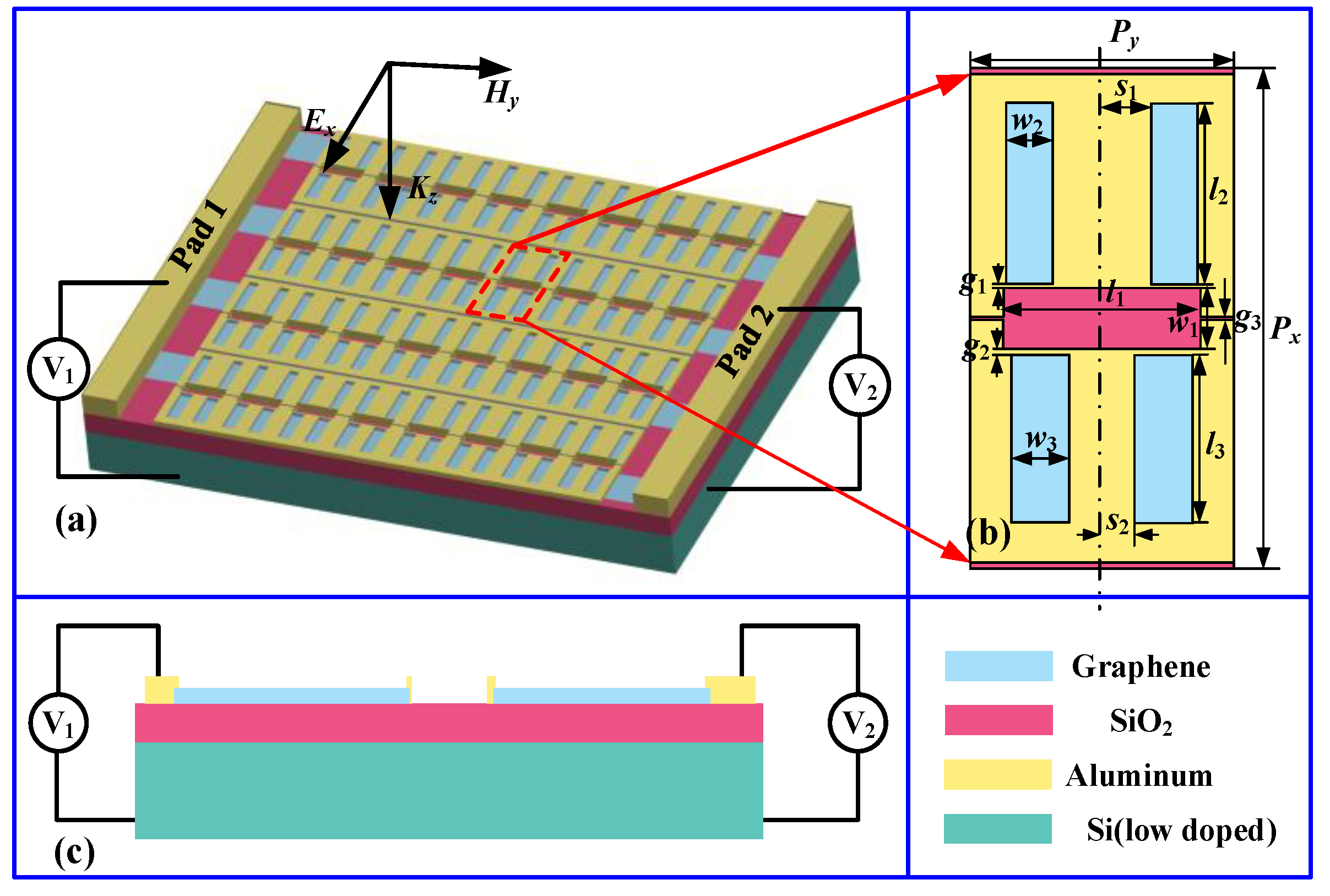
2. Structures, Materials and Methods
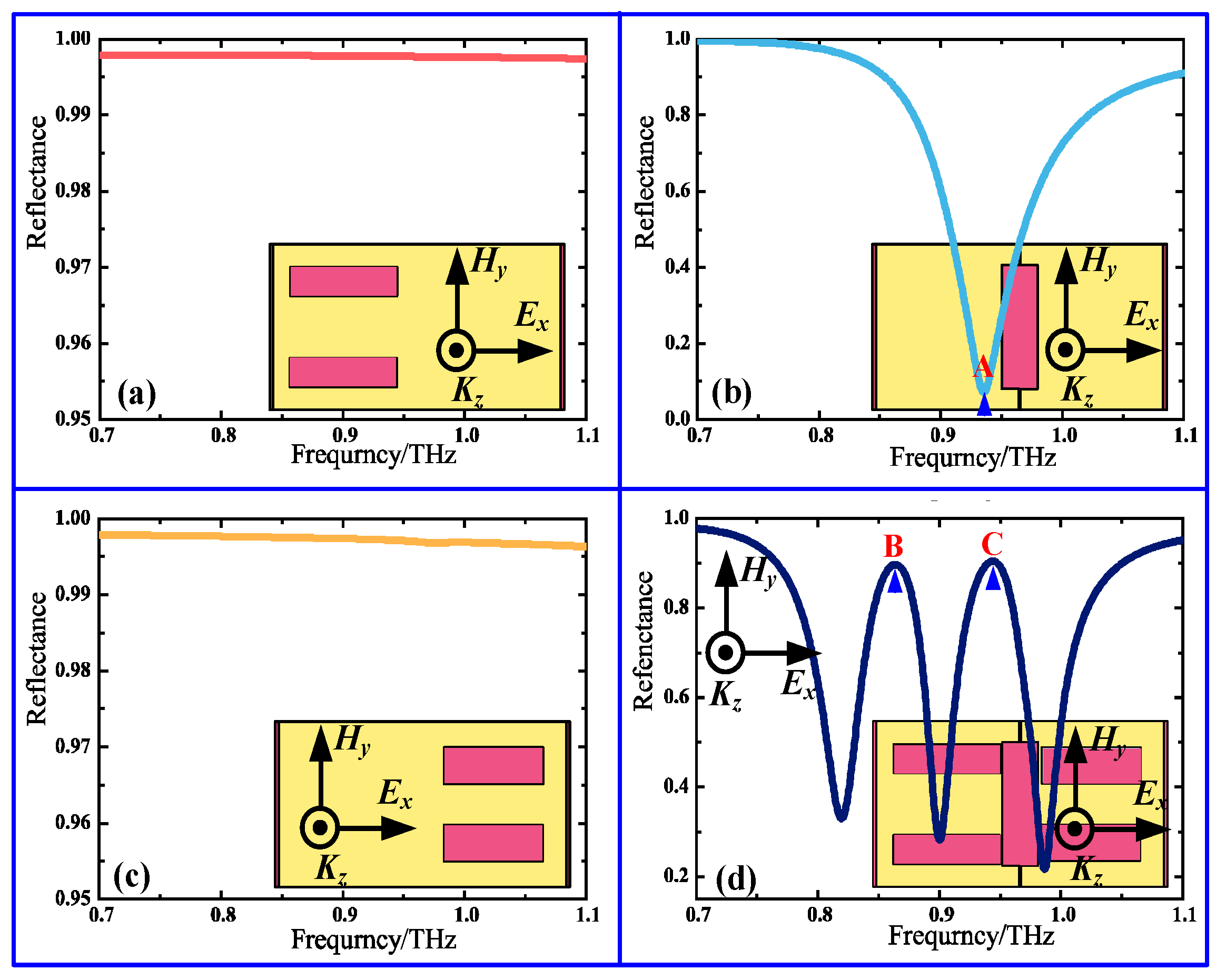
3. Evolution Mechanism of Two EIR Windows
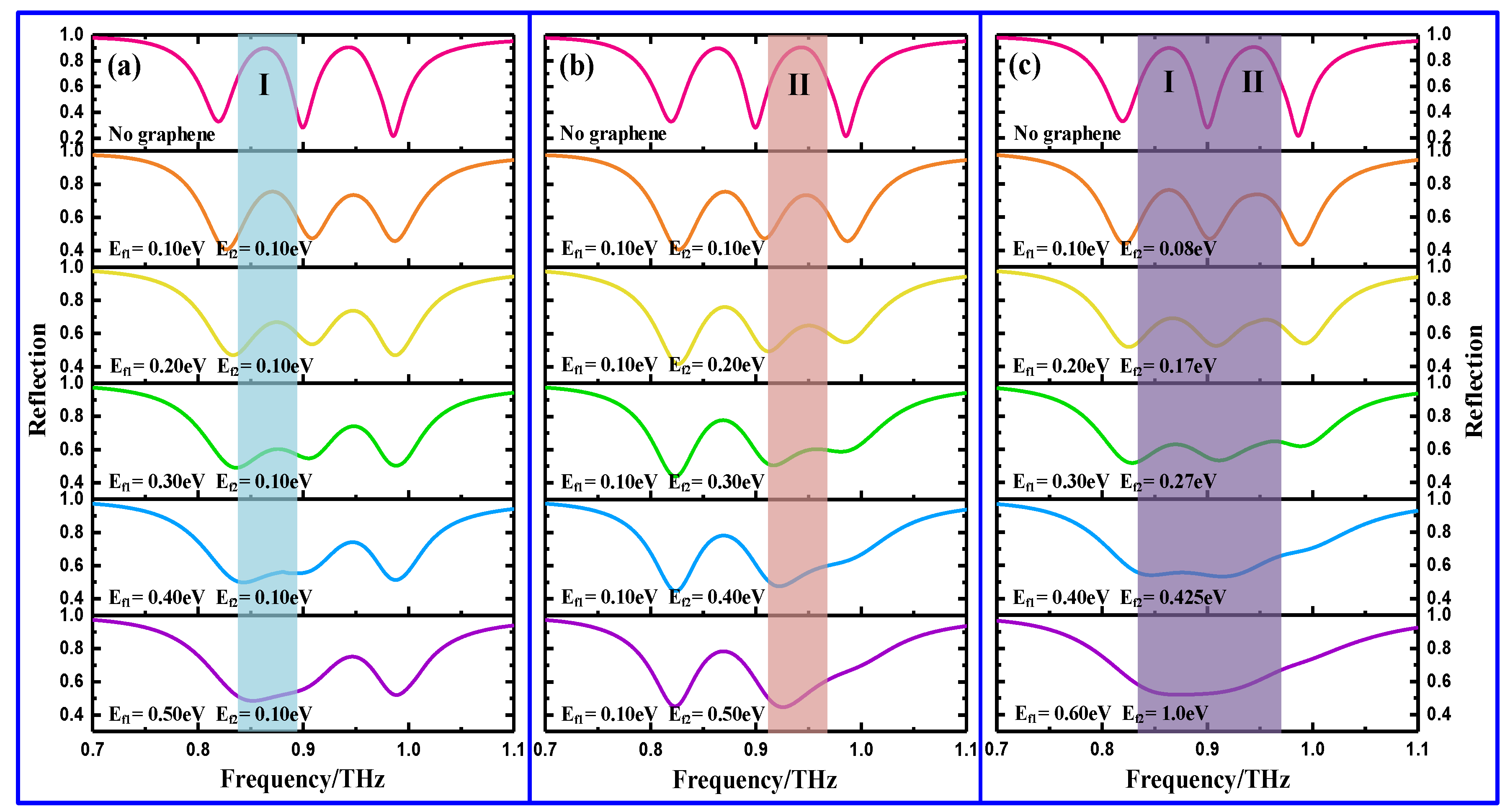
4. Selective and Active Modulation of Two EIR Windows
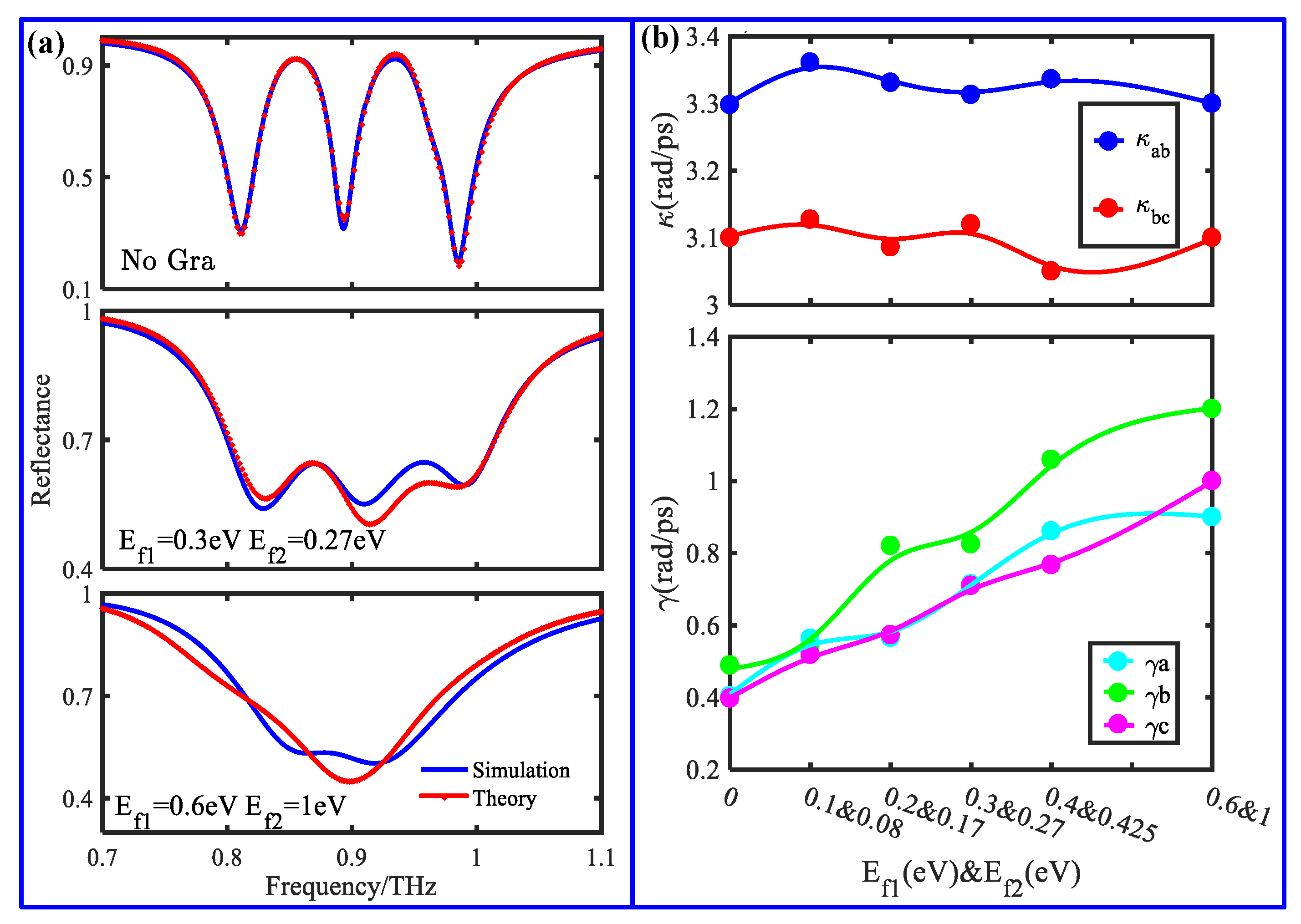
5. Tunable Slow-Light Applications
6. Conclusions
Author Contributions
Funding
Data Availability Statement
Conflicts of Interest
References
- Boller, K.J.; Imamolu, A.; Harris, S.E. Observation of electromagnetically induced transparency. Phys. Rev. Lett. 1991, 66, 2593–2596. [Google Scholar] [CrossRef] [Green Version]
- Hau, L.V.; Harris, S.E.; Dutton, Z.; Behroozi, C.H. Light speed reduction to 17 metres per second in an ultracold atomic gas. Nature 1999, 397, 594–598. [Google Scholar] [CrossRef]
- Zhang, Y.P.; Brown, A.W.; Xiao, M. Opening four-wave mixing and six-wave mixing channels via dual electromagnetically induced transparency windows. Phys. Rev. Lett. 2007, 99, 123603. [Google Scholar] [CrossRef] [Green Version]
- Fleischhauer, M.; Imamoglu, A.; Marangos, J.P. Electromagnetically induced transparency: Optics in coherent media. Rev. Mod. Phys. 2005, 77, 633. [Google Scholar] [CrossRef] [Green Version]
- Papasimakis, N.; Fedotov, V.A.; Zheludev, N.I. Metamaterial analog of electromagnetically induced transparency. Phys. Rev. Lett. 2008, 101, 253903. [Google Scholar] [CrossRef] [PubMed] [Green Version]
- Yang, Y.M.; Kravchenko, I.I.; Briggs, D.P.; Valentine, J. All-dielectric metasurface analogue of electromagnetically induced transparency. Nat. Commun. 2014, 5, 5753. [Google Scholar] [CrossRef] [Green Version]
- Devi, K.M.; Sarma, A.K.; Chowdhury, D.R.; Kumar, G. Plasmon induced transparency effect through alternately coupled resonators in terahertz metamaterial. Opt. Express 2017, 25, 10484–10493. [Google Scholar] [CrossRef]
- Yahiaoui, R.; Burrow, J.A.; Mekonen, S.M.; Sarangan, A.; Mathews, J.; Agha, I.; Searles, T.A. Electromagnetically induced transparency control in terahertz metasurfaces based on bright-bright mode coupling. Phys. Rev. B 2018, 15, 155403. [Google Scholar] [CrossRef] [Green Version]
- Chen, M.M.; Xiao, Z.Y.; Lu, X.J.; Lv, F.; Zhou, Y.J. Simulation of dynamically tunable and switchable electromagnetically induced transparency analogue based on metal-graphene hybrid metamaterial. Carbon 2020, 59, 273–282. [Google Scholar] [CrossRef]
- Xiao, B.G.; Tong, S.J.; Fyffe, A.; Shi, Z.M. Tunable electromagnetically induced transparency based on graphene metamaterials. Opt. Express 2020, 28, 4049. [Google Scholar] [CrossRef]
- Devi, K.M.; Chowdhury, D.R.; Kumar, G.; Sarma, A.K. Dual-band electromagnetically induced transparency effect in a concentrically coupled asymmetric terahertz metamaterial. J. Appl. Phys. 2018, 124, 063106. [Google Scholar] [CrossRef] [Green Version]
- Chen, M.M.; Xiao, Z.Y.; Lv, F.; Cui, Z.T.; Xu, Q.D. Dynamically tunable dual-band electromagnetically induced transparency-like in terahertz metamaterial. Opt. Mater. 2020, 107, 110060. [Google Scholar] [CrossRef]
- Chen, H.; Lu, W.B.; Liu, Z.G.; Geng, M.Y. Microwave Programmable Graphene Metasurface. ACS Photonics 2020, 7, 1425–1435. [Google Scholar] [CrossRef]
- Shamshirgar, A.S.; Hernández, R.E.R.; Tewari, G.C.; Fernández, J.F.; Ivanov, R.; Karppinen, M.; Hussainova, I. Functionally graded tunable microwave absorber with graphene-augmented alumina nanofibers. ACS Appl. Mater. Interfaces 2021, 13, 21613–21625. [Google Scholar] [CrossRef]
- Ioannidis, T.; Gric, T.; Rafailov, E. Surface plasmon polariton waves propagation at the boundary of graphene based metamaterial and corrugated metal in THz range. Opt. Quantum Electron. 2020, 52, 10. [Google Scholar] [CrossRef]
- Zhu, H.L.; Zhang, Y.; Ye, L.F.; Li, Y.K.; Xu, Y.H.; Xu, R.M. Switchable and tunable terahertz metamaterial absorber with broadband and multi-band absorption. Opt. Express 2020, 28, 38626–38637. [Google Scholar] [CrossRef] [PubMed]
- Ren, P.W.; Jia, Y.L.; Fan, C.Z. Investigation on Tunable and Enhanced Optical Properties with Graphene Metamaterials. J. Phys. Chem. C. 2020, 124, 21075–21081. [Google Scholar] [CrossRef]
- Gao, E.; Liu, Z.; Li, H.; Xu, H.; Zhang, Z.; Luo, X.; Xiong, C.; Liu, C.; Zhang, B.; Zhou, F. Dynamically tunable dual plasmon-inducedtransparency and absorption based on a single-layer patterned graphene metamaterial. Opt. Express 2019, 27, 13884. [Google Scholar] [CrossRef] [PubMed]
- Chen, X.; Fan, W.H. Polarization-insensitive tunable multiple electromagnetically induced transparencies analogue in terahertz graphene metamaterial. Opt. Mater. Express 2016, 6, 2607. [Google Scholar] [CrossRef]
- Zeng, C.; Cui, Y.D.; Liu, X.M. Tunable multiple phase-coupled plasmoninduced transparencies in graphene metamaterials. Opt. Express 2015, 23, 545. [Google Scholar] [CrossRef] [PubMed]
- Liu, T.T.; Wang, H.X.; Liu, Y.; Xiao, L.S.; Zhou, C.B.; Liu, Y.B.; Xu, C.; Xiao, S.Y. Independently tunable dual-spectral electromagnetically induced transparency in a terahertz metal-graphene metamaterial. J. Phys. D Appl. Phys. 2018, 51, 415105. [Google Scholar] [CrossRef] [Green Version]
- Liu, J.X.; Jin, K.L.; He, X.Y.; Zhang, W.J.; Lin, X.; Jin, Z.M.; Ma, G.H. Independently tunable dual-band plasmon induced transparency enabled by graphene-based terahertz metamaterial. Appl. Phys. Express 2010, 36, 1055–1063. [Google Scholar] [CrossRef]
- Zhang, K.; Liu, Y.; Wu, H.W.; Xia, F.; Kong, W.J. Dynamically selective control of dual-mode electromagnetically induced transparency in terahertz metal-graphene metamaterial. OSA Contin. 2020, 3, 505. [Google Scholar] [CrossRef]
- Manjappa, M.; Srivastava, Y.K.; Solanki, A.; Kumar, A.; Sum, T.C.; Singh, R. Hybrid lead halide perovskites for ultrasensitive photoactive switching in terahertz metamaterial devices. Adv. Mater. 2017, 29, 1605881. [Google Scholar] [CrossRef]
- Kim, J.; Son, H.; Cho, D.J.; Geng, B.; Regan, W.; Shi, S.; Kim, K.; Zettl, A.; Shen, Y.; Wang, F. Electrical control of optical plasmon resonance with graphene. Nano Lett. 2012, 12, 5598. [Google Scholar] [CrossRef] [Green Version]
- Vakil, A.; Engheta, N. Transformation optics using graphene. Science 2011, 332, 1291. [Google Scholar] [CrossRef] [PubMed] [Green Version]
- Hanson, G.W. Dyadic Green’s functions and guided surface waves for a surface conductivity model of graphene. J. Appl. Phys. 2008, 103, 064302. [Google Scholar] [CrossRef] [Green Version]
- Jnawali, G.; Rao, Y.; Yan, H.; Heinz, T.F. Observation of a transient decrease in terahertz conductivity of single-layer graphene induced by ultrafast optical excitation. Nano Lett. 2013, 13, 524. [Google Scholar] [CrossRef]
- Ergoktas, M.S.; Bakan, G.; Kovalska, E.; Fevre, L.W.L.; Fields, R.P.; Steiner, P.; Yu, X.; Salihoglu, O.; Balci, S.; Falko, V.I.; et al. Multispectral graphene-based electro-optical surfaces with reversible tunability from visible to microwave wavelengths. Nat. Photonics 2021, 15, 493–498. [Google Scholar] [CrossRef]
- Valmorra, F.; Scalari, G.; Maissen, C.; Fu, W.Y.; Schönenberger, C.; Choi, J.W.; Park, H.G.; Beck, M.; Faist, J. Low-bias active control of terahertz wave by coupling large-area CVD graphene to a terahertz metamaterial. Nano Lett. 2013, 13, 3193–3198. [Google Scholar] [CrossRef]
- Srivastava, Y.K.; Chaturvedi, A.; Manjappa, M.; Kumar, A.; Dayal, G.; Kloc, C.; Singh, R. MoS2 for ultrafast all-optical switching and modulation of THz fano metaphotonic devices. Adv. Opt. Mater. 2017, 5, 1700762. [Google Scholar] [CrossRef]
- Lu, H.; Liu, X.; Mao, D. Plasmonic analog of electromagnetically induced transparency inmulti-nanoresonator-coupled waveguide systems. Phys. Rev. A 2012, 85, 053803. [Google Scholar] [CrossRef]


Publisher’s Note: MDPI stays neutral with regard to jurisdictional claims in published maps and institutional affiliations. |
© 2021 by the authors. Licensee MDPI, Basel, Switzerland. This article is an open access article distributed under the terms and conditions of the Creative Commons Attribution (CC BY) license (https://creativecommons.org/licenses/by/4.0/).
Share and Cite
He, X.; Sun, C.; Wang, Y.; Lu, G.; Jiang, J.; Yang, Y.; Gao, Y. Graphene-Modulated Terahertz Metasurfaces for Selective and Active Control of Dual-Band Electromagnetic Induced Reflection (EIR) Windows. Nanomaterials 2021, 11, 2420. https://doi.org/10.3390/nano11092420
He X, Sun C, Wang Y, Lu G, Jiang J, Yang Y, Gao Y. Graphene-Modulated Terahertz Metasurfaces for Selective and Active Control of Dual-Band Electromagnetic Induced Reflection (EIR) Windows. Nanomaterials. 2021; 11(9):2420. https://doi.org/10.3390/nano11092420
Chicago/Turabian StyleHe, Xunjun, Chenguang Sun, Yue Wang, Guangjun Lu, Jiuxing Jiang, Yuqiang Yang, and Yachen Gao. 2021. "Graphene-Modulated Terahertz Metasurfaces for Selective and Active Control of Dual-Band Electromagnetic Induced Reflection (EIR) Windows" Nanomaterials 11, no. 9: 2420. https://doi.org/10.3390/nano11092420
APA StyleHe, X., Sun, C., Wang, Y., Lu, G., Jiang, J., Yang, Y., & Gao, Y. (2021). Graphene-Modulated Terahertz Metasurfaces for Selective and Active Control of Dual-Band Electromagnetic Induced Reflection (EIR) Windows. Nanomaterials, 11(9), 2420. https://doi.org/10.3390/nano11092420