Article

A Study on the Effects of Selenization Temperature on the Properties of Na-Doped Cu2ZnSn(S,Se)4 Thin Film and Its Correlation with the Performance of Solar Cells

1
Department of Life Sciences, Jilin Normal University, Siping 136000, China
2
Department of Physics, Jilin Normal University, Siping 136000, China
*
Author to whom correspondence should be addressed.
Nanomaterials 2021, 11(9), 2434; https://doi.org/10.3390/nano11092434
Submission received: 17 August 2021 / Revised: 15 September 2021 / Accepted: 15 September 2021 / Published: 18 September 2021
(This article belongs to the Section Synthesis, Interfaces and Nanostructures)

Abstract

:
In this study, we prepared Na-doped Cu2ZnSn(S,Se)4 [noted as (Na0.1Cu0.9)2ZnSn(S,Se)4] films on the Mo substrate using a simple and cheap sol–gel method together with the post-annealing technique. The effects of selenization temperature on the properties of Na-doped Cu2ZnSn(S,Se)4 were surveyed. The results indicated that some sulfur atoms in the films were substituted by selenium atoms by increasing the selenization temperature, and all films selenized at different temperatures had a kesterite structure. As the selenization temperature increased from 520 to 560 °C, the band gaps of the film can be tuned from 1.03 to 1 eV. The film with better morphology and opto-electrical properties can be obtained at an intermediate selenization temperature range (e.g., 540 °C), which had the lowest resistivity of 47.7 Ω cm, Hall mobility of 4.63 × 10⁻¹ cm2/Vs, and carrier concentration of 2.93 × 1017 cm−3. Finally, the best power conversion efficiency (PCE) of 4.82% was achieved with an open circuit voltage (Voc) of 338 mV, a short circuit current density (Jsc) of 27.16 mA/cm2 and a fill factor (FF) of 52.59% when the selenization temperature was 540 °C.

1. Introduction

Cu2ZnSn(S,Se)4 (CZTSSe) is a helpful absorber layer for high reserves and inexpensive thin film solar cells because of its appropriate semiconductor characteristics having a tunable band gap, p-type conduction characteristics, and high absorption coefficient [1,2,3]. Furthermore, it can be considered as a substitute to Cu(In, Ga)Se2 and CuInS2 absorbers, in which the extremely rare and expensive indium (In) is substituted by abundant and environmentally friendly zinc (Zn) and tin (Sn) [4,5,6]. At present, studies on Cu2ZnSnS4 (CZTS)-based solar cells are still in their infancy, with the highest reported PCE of 12.62% [7], which is far below the theoretical PCE of 32.2% [8], and at the same time, it also is far behind the PCE (22.9%) of CuInGaSe2 (CIGSe) counterparts [9]. The PCE of CZTS-based solar cells has not been greatly improved in recent years. There are several factors impeding the efficiency of further improvement for CZTSSe solar cells, including the crystal quality and optoelectronic properties of the CZTSSe semiconductors, as well as the energy band matching between the CZTSSe and CdS interface [10,11,12,13]. Recent research has shown that the fabrication of adjustable band gap absorbers is a practical way to solve the band matching of CdS and CZTSSe heterojunction interfaces and improve cell efficiency. Therefore, many studies on cationic replacement have been performed to adjust the band gap of the CZTSSe, for instance, GeSn and AgCu [14,15,16]. Although GeSn and AgCu can modulate the band gap of the CZTS, they are too expensive to be used as an ideal absorbing layer material for future commercial production. It was reported that the band gap of the CZTSSe was successfully adjusted by Na doping. In addition, Na doping can significantly improve the crystallization quality and optical–electrical characteristic of CZTSSe [17,18]. These similar results about Na doping have been observed in our previous work. Compared to Ge and Ag, the Na is cheaper, plentiful, and environmentally friendly. Thus, it is deduced that Na-doped Cu2ZnSn(S,Se)4 is more worthy of studying as a potential absorbing layer material.
It is well known that in order to obtain CZTSSe films with a single phase and uniform dense grains, the precursor film prepared by spin coating is usually heat-treated at a higher temperature. This indicated that the selenization temperature of the film plays a very important role in enhancing performance, such as crystal quality and photoelectric properties [19,20,21]. The impact of the selenization temperature on the optical-electrical characteristic of CZTSSe has been widely researched [22,23,24]. However, the impacts of the selenization temperature on the structural and photoelectric characteristic of Na-doped Cu2ZnSn(S,Se)4 films have not been researched to this day. In this work, we have reported the preparation of highly crystalline Na-doped Cu2ZnSn(S,Se)4 films utilizing a sol–gel spin-coating technique together with the selenization process. In addition, the impact of the selenization temperature on the structure and optoelectronic properties of Na-doped Cu2ZnSn(S,Se)4 as well as the device performance have been investigated in detail.

2. Experimental Details

2.1. Preparation of (Na0.1Cu0.9)2ZnSn(S,Se)4 Film

For the preparation of Na-doped Cu2ZnSn(S,Se)4 films, the precursor solution was obtained by dissolving copper (II) acetate monohydrate (5.400 × 10⁻³ mol), tin (II) chloride dihydrate (3.750 × 10⁻³ mol), zinc acetate (4.396 × 10⁻³ mol), sodium chloride (0.600 × 10⁻³ mol), thiourea (3 × 10⁻² mol) and monoethanolamine (MEA) in dimethyl sulfoxide. The precursor solution was incessantly stirred at a temperature of 45 °C to make the metal compounds completely dissolve. Thereafter, the solution was spun onto the Molybdenum-coated soda lime glasses (SLGs) at a speed of 3000 rpm for 30 s, then the substrate was dried at 300 °C in the air atmosphere. In the end, the Na-doped Cu2ZnSn(S,Se)4 precursor films were annealed at different temperatures for 15 min in the selenium atmosphere.

2.2. Device Fabrication

The Na-doped Cu2ZnSn(S,Se)4 thin films were prepared by spin coating a precursor solution onto a Mo-coated Na-free substrate, then the film was annealed at 540 °C for 15 min in an Se atmosphere. The CdS buffer layer was synthesized using a chemical-bath deposition (CBD). The reaction was accomplished in 190 mL of deionized water with 51.3 mg of Cd(SO)4, 10.7 mg NH4Cl, 10 mL NH3·H2O, and 76.12 mg thiourea at 75 °C for 14 min. The intrinsic zinc oxide/aluminum zinc oxide (AZO) was deposited as a transparent conducting layer by using a sputtering system. The Ag gate electrode (9 devices per substrate) was then evaporated to complete the device fabrication. The prepared devices were mechanically scribed into nine areas of a 0.19 cm2 area.

2.3. Characterization

Diffraction patterns of the selenized Na-doped Cu2ZnSn(S,Se)4 were measured using X-ray power diffraction (XRD, Rigaku Corporation, Tokyo, Japan) and equipped Cu Kα radiation. Raman spectra were surveyed with an excitation wavelength of 514 nm. The chemical component analysis of the films was measured by X-ray photoelectron spectroscopy (XPS; Thermo Fisher Scientific, Waltham, MA, USA) and energy-dispersive X-ray spectroscopy (EDS, JEOL Ltd., Tokyo, Japan). SEM and TEM images were taken using an FEI Nova NanoSEM 230 (Hitachi S-4800, JEOL Ltd., Tokyo, Japan). The electrical properties were performed by a Hall measurement system (Hall, Lakershore HMS 7707, Irvine, CA, USA). The optical spectra were measured using UV–Vis–NIR spectra. The external quantum efficiency (EQE) spectrum was measured using SPIQE200-5324 (QEX10, Newport, Irvine, CA, USA) in air. The current density–voltage characteristics (J–V) of Na-doped Cu2ZnSn(S,Se)4 solar cells were measured using a 94043A I-V Station under simulated AM 1.5G solar irradiation at a light intensity of 100 mW/cm2 (Model 91160, Newport, Irvine, CA, USA).

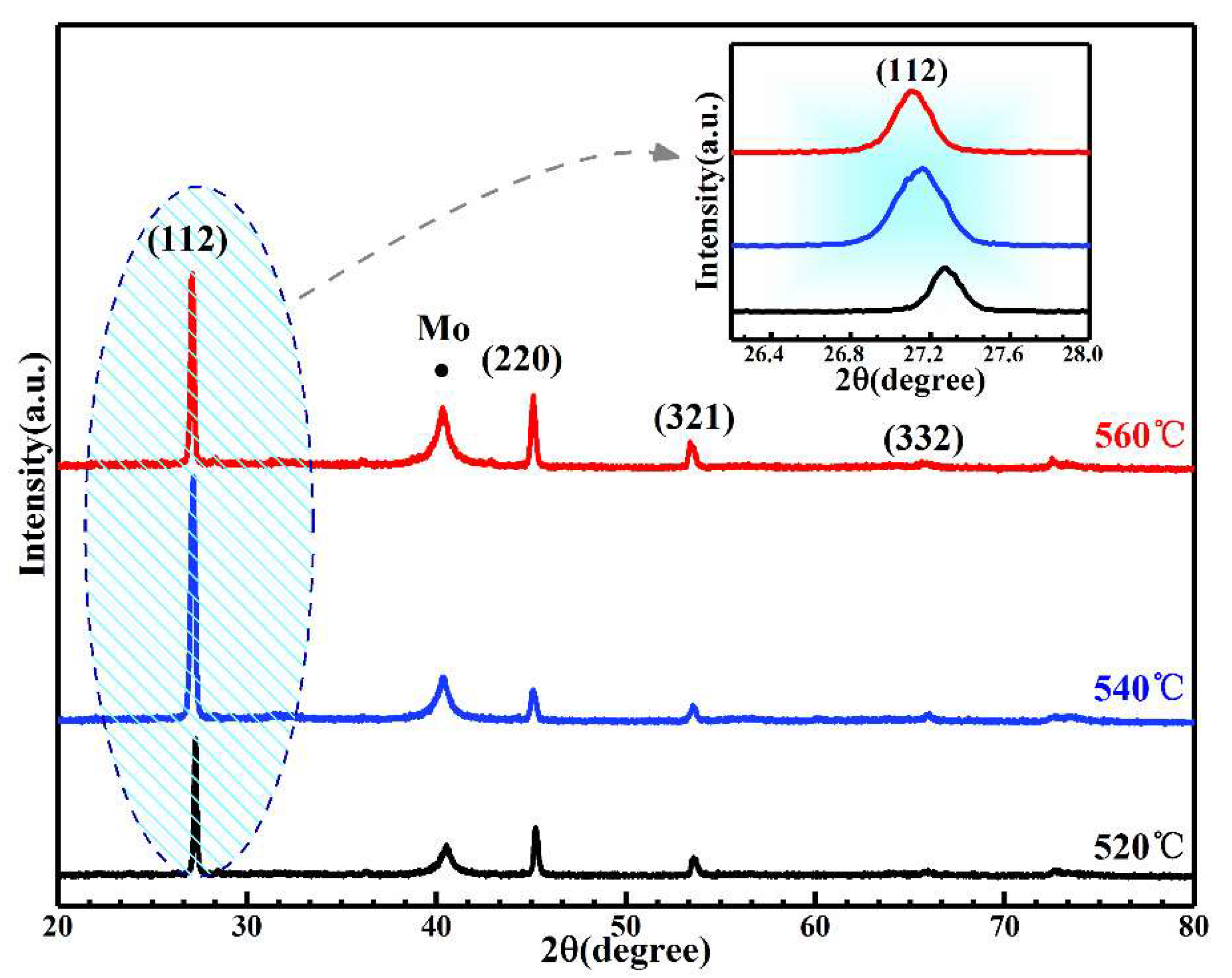
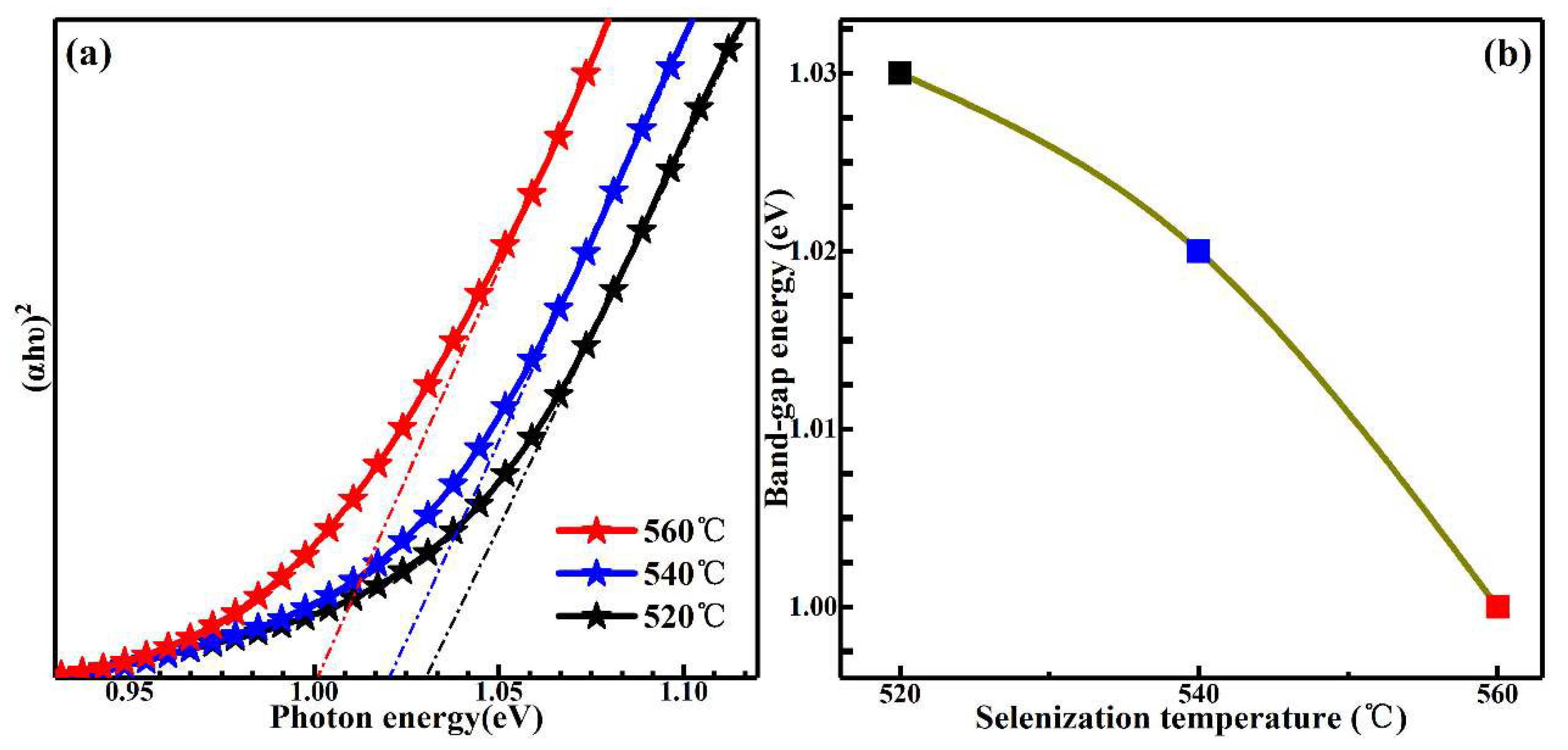
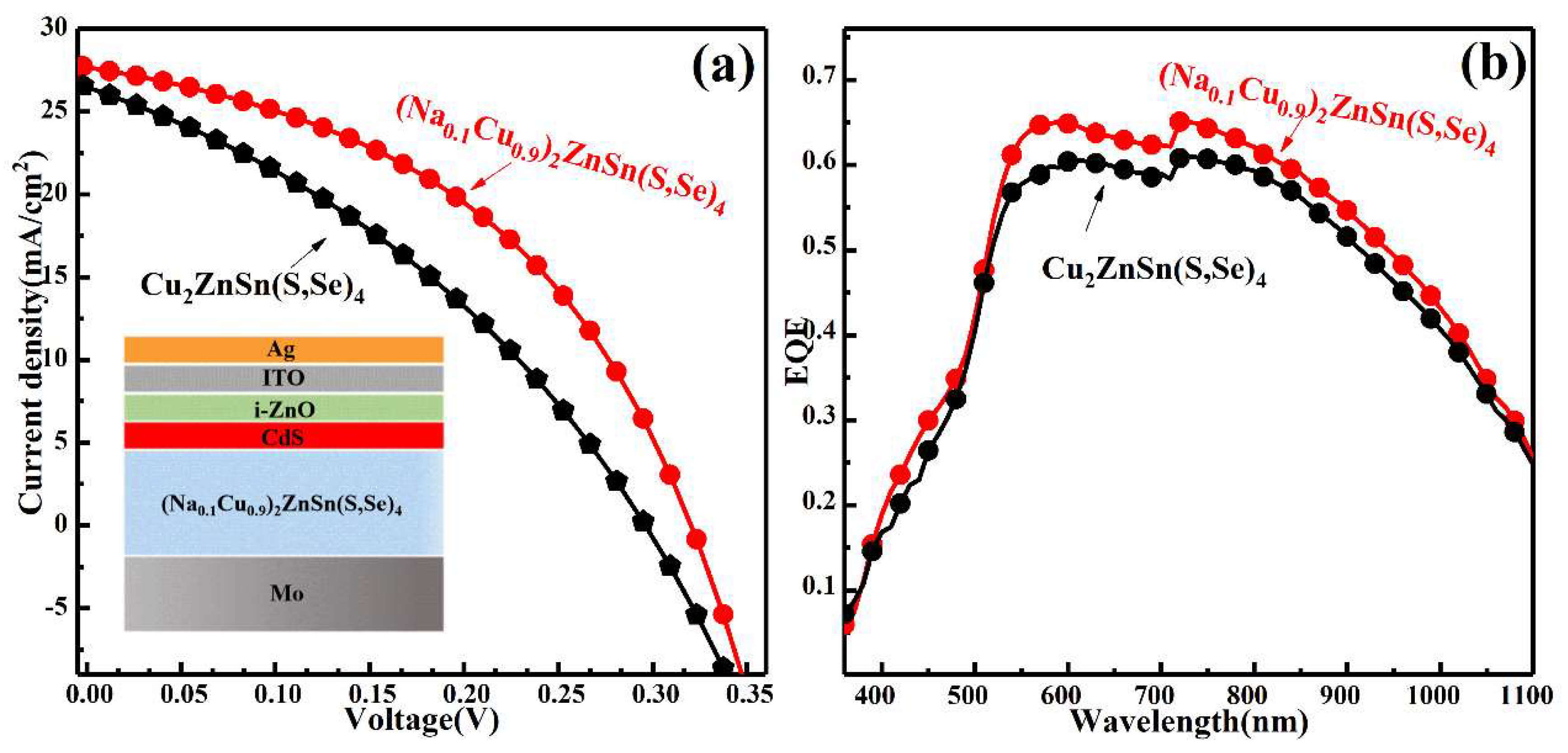
3. Results and Discussion

Figure 1 displays the XRD patterns of the three (Na0.1Cu0.9)2ZnSn(S,Se)4 annealed at the temperatures of 520, 540, and 560 °C (labeled as samples T520, T540, and T560). For all films, five distinct diffraction peaks, located at 27.27°, 45.20°, 53.61°, 66.04°, and 72.70° other than Mo peak (40.53°), can be observed and corresponded to the diffraction peaks of the (112), (220), (312), (008) and (323) lattice planes of the CZTS with kesterite structures [25,26]. Except for the CZTS and Mo diffraction peaks, no other secondary phase was detected, implying that kesterite structures (Na0.1Cu0.9)2ZnSn(S,Se)4 were successfully synthesized. In addition, it is observed that the intensity of the (112) peaks for the film selenized at 540 °C is larger than that of other samples, indicating the diffraction peak intensity increases and then decreases with the selenization temperature increasing. This may be because of the increase in the selenization temperature; the grains in the thin films grew stably as they increasingly obtained more energy. Thus, the intensity of the diffraction peak became larger. However, when the selenization temperature increased to a certain value, some atoms had adequate energy to escape from the thin films, which made the defects increase in the thin films. Thus, the peaks’ intensity became weak. We can explore the impact of selenization temperature on the lattice constant by observing the move of the diffraction angle. As shown in the inset of Figure 1, the change in the diffraction angle is linearly dependent on the annealing temperature. All (112) diffraction peaks shifted to small diffraction angles with increased selenization temperatures. Because the decrease in diffraction angles stands for the increase in the lattice distance, it is attributed that plenty of Se occupied the position of S with the temperature increase, which is proven in the EDX results later. These results show that the crystal structure of Na-doped Cu2ZnSn(S,Se)4 is not changed with the change in the selenization temperature, and when the selenization temperature reached 540 °C, the crystal quality was optimal.
As everyone knows, the detection of the kesterite CZTSSe merely by XRD is not easy, because the XRD feature peaks of the kesterite CZTSSe with some impurity phase chalcogenides are almost overlapped [27]. Therefore, to further determine the purity of the phase and the crystal quality of the Na-doped Cu2ZnSn(S,Se)4 films, it is usually necessary to characterize the Raman spectrum. Figure 2 depicts the Raman spectroscopy of the Na-doped Cu2ZnSn(S,Se)4 annealed at different temperatures of 520, 540, and 560 °C (labeled as samples T520, T540, and T560, respectively). The three Raman peaks at 175, 196, and 337 cm−1 match the Raman characteristic vibrational A2, A1, and E modes of the kesterite CZTSSe phase [28,29,30]. No Raman peaks of some possible secondary phases were detected for Na-doped Cu2ZnSn(S,Se)4 films at different temperatures. This result also confirmed the formation of pure phase Na-doped Cu2ZnSn(S,Se)4. The illustration in Figure 2 presents the change in the peak location of the A1 mode. As shown in the inset, the A1 mode peaks slightly move to a lower wave value with the selenization temperature increasing, which may be ascribed to the replacement of some larger Se for S in the lattice with the increased temperature, leading to the expanding of the lattice constant, which is in agreement with the XRD result.
The bonding states of the constituent chemical elements of the Na-doped Cu2ZnSn(S,Se)4 film selenized at 540 °C were studied by XPS measurements. As shown in Figure 3, the peaks corresponding to Cu 2p, Zn2p, Sn3d, S2p, Se3d, and Na1s were observed. Figure 3a presents the Cu 2p XPS spectra (green curve). The peaks at 950.75 and 930.88 eV accord with Cu 2p1/2 and Cu 2p3/2, and the interval value of the peaks is 19.87 eV. This indicates that Cu is present only in a Cu+ state [31]. Figure 3b reveals Zn 2p XPS spectra (red curve), two peaks situated at 1043.62 and 1020.58 eV were attributed to Zn 2p 1/2 and Zn 2p 3/2 peaks, respectively, and the binding energy interval is 23.04 eV, implying that Zn exists in the oxidation state of Zn2+ [32]. Figure 3c shows the XPS spectra of Sn 3d (blue curve), the peaks situated at 493.99 and 485.50 eV corresponding to Sn 3d 3/2 and Sn 3d 5/2, and the binding energy interval is 8.49 eV, indicating that Sn is presented in the oxidation state of Sn4+ [33]. The high-resolution spectra of the S 2p and the Se 3p peaks are displayed in Figure 3d. Due to the overlapping of the S 2p and the Se 3p core level, the XPS spectra were deconvoluted using a Gaussian fitting method. Four peaks lie at 158.86, 159.53, 160.38 and 165.02 eV, corresponding to the Se 3p 3/2, S 2p 3/2, S 2p 1/2, and Se 3p 1/2 peaks (yellow, red, blue and green curves), respectively. The peaks of S 2p 3/2 and S 2p 1/2 appeared at 159.53 and 160.38 eV, consistent with the standard reference value of S2− [34]. As shown in Figure 3e, the XPS spectra of Se 3d were fitted by two peaks (green and blue curves) situated at 53.23 and 53.97 eV using a Gaussian fitting method. The two peaks are ascribed to Se 3d 3/2 and Se 3d 1/2, respectively, implying that the Se valence state is 2- [34]. Figure 3f presents the XPS spectrum (orange curve) of Na 1s with the peak at 1070.49 eV, suggesting the existence of monovalent Na+ in Na-doped Cu2ZnSn(S,Se)4 film [25]. The results of the XPS show that the Na-doped Cu2ZnSn(S,Se)4 film with the constituent element in the form of Cu+, Zn2+, Sn4+, S2, Se2 and Na+ has been successfully synthesized.
The TEM measurements were carried out to further clarify the specific microscopic structure of the Na-doped Cu2ZnSn(S,Se)4 film. Figure 4a,b display the TEM images of Cu2ZnSn(S,Se)4 and Na-doped Cu2ZnSn(S,Se)4 films selenized at 540 °C, respectively. The lattice streaks are distinctly observed in Figure 4a, and the lattice fringes with an interplanar spacing of 0.406 nm were put down to the (112) planes of kesterite CZTSSe [35]. As shown in Figure 4b, for the Na-doped Cu2ZnSn(S,Se)4 film, the fringe spacing evidently increased to 0.474 nm. CZTSSe interplanar spacing (0.406 nm) smaller than that (0.474 nm) of Na-doped Cu2ZnSn(S,Se)4 indicated an enlargement of the lattice due to the substitution of some Cu with Na atoms. According to the above results, it is inferred that Na replaced some Cu in the CZTSSe crystal lattice. TEM images indicate that we have obtained Na-doped Cu2ZnSn(S,Se)4 film with a highly uniform nanostructure, which is an important prerequisite for obtaining CZTSSe-based thin film solar cells with a higher efficiency.
It is well known that the chemical composition of the absorbing layer films influences device performance. Table 1 presents the EDS measurement results of the samples annealed at the different temperatures of 520, 540, and 560 °C (labeled as samples T520, T540, and T560, respectively). It was recognized that the atomic percentage of S evidently reduced from 8.47 to 2.08, and the atomic percentages of Se rose from 43.47 to 46.64 as the annealing temperatures varied from 520 °C to 560 °C. Hence, it was deduced that the atomic percentages of Se increased with the selenization temperatures increasing. Moreover, it can be acknowledged that the change in the atomic percentage for other elements (Cu, Zn, Na and Sn) was only slight in comparison to the variation in the contents of Se and S. The percentages of Se/(S+Se) were 83.69, 91.49, and 97.74 when the selenization temperatures are 520, 540 and 560 °C, respectively. This result directly provides evidence for the introduction of Se atoms into the lattice by high-temperature selenization, which verifies the conclusion that more Se was substituted for S as the selenization temperature increased in the above analysis results.
The SEM surface images of the Cu2ZnSn(S,Se)4 selenized at 540 °C and the SEM images of the Na-doped Cu2ZnSn(S,Se)4 selenized at the different temperatures of 520, 540 and 560 °C displayed in Figure 5a–d. As displayed in Figure 5a, the surface morphology of the CZTSSe showed a relatively rough surface and irregular small grain of 500–800 nm. Figure 5b displays the surface morphology of the Na-doped Cu2ZnSn(S,Se)4 thin film selenized at 520 °C. Enhanced grain growth in the film was observed when Na was introduced, as the grain size was significantly enlarged to around 500 nm. When the selenization temperature increased to 540 °C, the evident morphological change of grain was observed. As displayed in Figure 5c, the crystalline size increased significantly to 1.0–2.5 μm, and the surface morphology was flat and dense. However, when the selenization temperature continually increased to 560 °C, the size of the crystal particle significantly decreased and the surface became rough, as displayed in Figure 5d. These results manifest that the optimum selenization temperature is 540 °C, which offers beneficial selenization surroundings to facilitate grain growth resulting in the formation of the compact thin film.
To survey the impact of selenization temperatures on the optical band gaps of Na-doped Cu2ZnSn(S,Se)4, the optical absorption of the samples were obtained by a UV–VIS–NIR spectrophotometer. On the basis of the solid band theory, the relational expression between the energy of the incident ray () and the absorption coefficient (α) can be expressed as:
(αhυ) = B(Eg)n
where h is the Plank’s constant, B is the band edge constant, and Eg is the optical band gap. The value of n is 1/2, since CZTS is a direct band gap semiconductor [36]. The relationship of (αhυ)2 versus for (Na0.1Cu0.9)2ZnSn(S,Se)4 has been shown in Figure 6a. Utilizing the data in Figure 6a and Equation (1), the band gaps are estimated to be 1.03, 1.02, and 1.00 eV for samples selenized at temperatures of 520, 540 and 560 °C, respectively. As shown in Figure 6b, we can clearly see that the band gaps show a declining trend. Combined with the XRD, Raman, TEM and EDS results, it is concluded that as the selenization temperature increased, the reduction in band gaps is ascribed to the change in lattice and difference in electronegativity due to alloying, as well as the modification of atomic structure owing to Se replacing the site of S. The adjustable band gap of Na-doped Cu2ZnSn(S,Se)4 film is of extraordinary importance for enhancing the performance of solar cells.
Table 2 lists the electrical properties of the films measured by Hall measurement. It is recognized that all Na-doped Cu2ZnSn(S,Se)4 films selenized at different temperatures show p-type conduction behaviors. When the selenization temperature increased, the carrier concentration first increased rapidly and then decreased slightly, and the carrier concentration reached a maximum value with 2.93 × 1017 cm−3 at the temperature of 540 °C. However, the resistivity first reduced rapidly and then rose slightly with the selenization temperature increasing, and reached a minimum value of 47.7 Ωcm at the temperature of 540 °C. Combined with the results of SEM, it was deduced that when the annealing temperature was increased from 520 to 540 °C, the crystal quality of the films was improved, the defects at the surface of films were passivated, and the resistivity and carrier concentration achieved the optimum value at the temperature of 540 °C. However, as the selenization temperature further increased from 540 to 560 °C, the surface morphology and crystallinity of the films began to deteriorate, leading to the resistivity and carrier concentration of the films worsening. By increasing the selenization temperature from 520 to 600 °C, the mobility decreased from 4.63 × 100 cm2V−1S−1 to 4.63 × 10⁻¹ cm2V−1S−1 and then increased to 2.57 × 100 cm2V−1S−1. It is well known that conductivity is proportional to the product of mobility and carrier concentration, and for semiconductors, the behavior of a material can be very different depending on whether there are many carriers with low Hall mobility, or few electrons with high Hall mobility. In the present work, according to the Hall measurement results, it was observed that the change in mobility is indeed opposite to that of carrier concentration with the change in selenization temperatures. Finally, it was found that when the film was selenized at 540 °C, the electrical conductivity of Na-doped Cu2ZnSn(S,Se)4 film reached its optimal state with the lowest resistivity of 47.7 Ωcm, Hall mobility of 4.63 × 10⁻¹cm2/Vs, carrier concentration of 2.93 × 1017 cm−3, and the film had higher carriers with low mobility. Thus, it implied that the selenization temperature of 540 °C may be more advantageous as this temperature supplied better annealing surroundings to form Na-doped Cu2ZnSn(S,Se)4 film.
According to the above results, it was found that the Na-doped Cu2ZnSn(S,Se)4 film had better crystallinity and opto-electrical properties at the temperature of 540 °C, which are regarded suitable as the absorbed layer. Thus, it was regarded as the absorbed layer to fabricate a solar cell. Figure 7a displays the current density (J) against voltage (V) curves of the corresponding CZTSSe and (Na0.1Cu0.9)2ZnSn(S,Se)4 solar cells fabricated under the same experimental conditions. The illustration of Figure 7 shows a structural sketch of the device (SLG/Mo/(Na0.1Cu0.9)2ZnSn(S,Se)4/CdS/ZnO/ITO/Al) with a traditional cell structure. The detailed performance parameters of the two devices are presented in Table 3. The CZTSSe device exhibits a Voc of 296 mV, a Jsc of 26.42 mA/cm2, an FF of 35.16%, and a PCE of 2.75%. However, the (Na0.1Cu0.9)2ZnSn(S,Se)4 device showed a PCE of 4.82% with Voc of 338 mV, Js of 27.16 mA/cm2, and FF of 52.59%. The Voc, Jsc, and FF values of Na-doped Cu2ZnSn(S,Se)4 solar cells were enhanced compared with that of CZTSSe solar cells. According to the J–V curve graph, the shunt resistance (RSH) was evaluated to be ~130.80 Ω·cm2 and the series resistance (RS) was ~30.37 Ω·cm2 in the CZTSSe device, whereas RSH is evaluated to be ~279.05 Ω·cm2 and RS is ~17.58 Ω·cm2 for the Na-doped Cu2ZnSn(S,Se)4 solar cell. The increase in shunt resistance and decrease in series resistance is a consequence of the increase in crystal particle size and decrease in defect density in the Na-doped Cu2ZnSn(S,Se)4 device. These enhancements in shunt and series resistance led to the improvement of the current density and fill factor. The tendency of Jsc, FF and Voc resulted in the increase in PCE from ~2.75% to ~4.82%, suggesting that Na doping can enhance the performance of solar cells. To survey the spectral response and in-depth understanding of the performance improvement of the device’, the spectral responses EQE was measured for CZTSSe and (Na0.1Cu0.9)2ZnSn(S,Se)4 device, as displayed in Figure 7b. The EQE data were enhanced in the entire visible region for the Na-doped Cu2ZnSn(S,Se)4 device, which can be interpreted by the increased Rsh and reduced RS, compared to the CZTSSe device. The results also revealed the preferable light carrier collection in Na-doped Cu2ZnSn(S,Se)4 solar cells, which was much enhanced in comparison with that of CZTSSe solar cells. Therefore, compared with the CZTSSe, the device obtained by using Na-doped Cu2ZnSn(S,Se)4 as the absorption layer had a better performance. Although there is still a discrepancy between the achieved efficiency and reported record efficiency, we will mainly explore and optimize the experimental condition of each part in the device structure to achieve the highly powered conversion efficiency for Na-doped Cu2ZnSn(S,Se)4 solar cells in our subsequent work.

4. Conclusions

The Na doping method has proven to be promising in the preparation of CZTS-based solar cells. The Na-doped Cu2ZnSn(S,Se)4 films were obtained at different selenization temperatures by the sol–gel method together with the rapid annealing technique. The crystallinity, electrical, and optical properties of Na-doped Cu2ZnSn(S,Se)4 films were highly influenced by the selenization temperatures. The annealing temperature of 540 °C supplied favorable selenization surroundings to promote the growth of the grain which brought about the formation of the compact thin film. The Eg of Na-doped Cu2ZnSn(S,Se)4 films can be tuned from 1.03 to 1 eV by an increase in the annealing temperature from 520 to 560 °C. All Na-doped Cu2ZnSn(S,Se)4 thin films had p-type conduction characteristics, and the films with better electrical properties were obtained by adjusting the selenization temperature. In the end, the Na-doped Cu2ZnSn(S,Se)4 film possessing the preferable crystallinity as well as optical and electrical properties, was acquired at the optimal selenization temperature of 540 °C, which was regarded as the absorbed layer to prepare the solar cell, achieving a PCE of 4.82%. Therefore, the selenization temperature of 540 °C can be more advantageous to synthesize the Na-doped Cu2ZnSn(S,Se)4 solar cells because this temperature supplies favorable annealing surroundings to form a Na-doped Cu2ZnSn(S,Se)4 absorber.

Author Contributions

Conceptualization, Z.W. and Y.S.; Writing—Original Draft Preparation, D.J.; Software, F.Z.; Formal Analysis, Z.W. and Y.S.; Investigation, Y.S. and D.J.; Writing—Review and Editing, Z.W. and F.Z. All authors have read and agreed to the published version of the manuscript.

Funding

This research was funded by the National Natural Science Foundation of China under Grant No. 61,505,067.

Institutional Review Board Statement

Not applicable.

Informed Consent Statement

Informed consent was obtained from all subjects involved in the study.

Conflicts of Interest

The authors declare no conflict of interest.

References

  1. Todorov, T.K.; Reuter, K.B.; Mitzi, D.B. High-efficiency solar cell with earth-abun-dant liquid-processed absorber. Adv. Mater. 2010, 22, E156–E159. [Google Scholar] [CrossRef]
  2. Kaur, K.; Kumar, N.; Kumar, M. Strategic review of interface carrier recombination in earth abundant Cu–Zn–Sn–S–Se solar cells: Current challenges and future prospects. J. Mater. Chem. A 2017, 5, 3069–3090. [Google Scholar] [CrossRef]
  3. Panthani, M.G.; Akhavan, V.; Goodfellow, B.; Schmidtke, J.P.; Dunn, L.; Dodabalapur, A.; Barbara, P.F.; Korgel, B.A. Synthesis of CuInS, CuInSe, and Cu(InxGa1-x)Se(CIGS) Nanocrystal “Inks” for Printable Photovoltaics. J. Am. Chem. Soc. 2008, 130, 16770–16777. [Google Scholar] [CrossRef] [PubMed]
  4. Lokhande, A.C.; Chalapathy, R.B.V.; He, M.; Jo, E.; Gang, M.; Pawar, S.A.; Lokhande, C.D.; Kim, J.H. Development of Cu2SnS3 (CTS) thin film solar cells by physical techniques: A status review. Sol. Energy Mater. Sol. Cells 2016, 153, 84–107. [Google Scholar] [CrossRef]
  5. Jackson, P.; Hariskos, D.; Wuerz, R.; Kiowski, O.; Bauer, A.; Friedlmeier, T.M.; Powalla, M. Properties of Cu(In,Ga)Se2 solar cells with new record efficiencies up to 21.7%. Phys. Status Solidi 2015, 9, 28–31. [Google Scholar] [CrossRef]
  6. Park, J.Y.; Chalapathy, R.B.V.; Lokhande, A.C.; Hong, C.W.; Kim, J.H. Fabrication of earth abundant Cu2ZnSnSSe4 (CZTSSe) thin film solar cells with cadmium free zinc sulfide (ZnS) buffer layers. J. Alloys Compd. 2017, 695, 2652–2660. [Google Scholar] [CrossRef]
  7. Son, D.H.; Kim, S.H.; Kim, S.Y.; Kim, Y.I.; Sim, J.H.; Park, S.N.; Jeon, D.H.; Hwang, D.K.; Sung, S.J.; Kang, J.K.; et al. Effect of solid-H2S gas reactions on CZTSSe thin film growth and photovoltaic properties of a 12.62% efficiency device. J. Mater. Chem. A 2019, 7, 25279–25289. [Google Scholar] [CrossRef] [Green Version]
  8. Shockley, W.; Queisser, H.J. Detailed balance limit of efficiency of p–n junction solar cells. J. Appl. Phys. 1961, 32, 510–519. [Google Scholar] [CrossRef]
  9. Kato, T.; Wu, J.L.; Hirai, Y.; Sugimoto, H.; Bermudez, V. Record Efficiency for Thin Film Polycrystalline Solar Cells Up to 22.9% Achieved by Cs-Treated Cu(In,Ga)(Se,S)2. IEEE J. Photovolt. 2018, 9, 325–330. [Google Scholar] [CrossRef]
  10. Wang, W.; Winkler, M.T.; Gunawan, O.; Gokmen, T.; Todorov, T.K.; Zhu, Y.; Mitzi, D.B. Device Characteristics of CZTSSe Thin-Film Solar Cells with 12.6% Efficiency. Adv. Energy Mater. 2014, 4, 1301465. [Google Scholar] [CrossRef]
  11. Tanaka, K.; Oonuki, M.; Moritake, N.; Uchiki, H. Cu2ZnSnS4 thin film solar cells prepared by non-vacuum processing. Sol. Energy Mater. Sol. Cells 2009, 93, 583–587. [Google Scholar] [CrossRef]
  12. Rey, G.; Redinger, A.; Sendler, J.; Weiss, T.P.; Thevenin, M.; Guennou, M.; El Adib, B.; Siebentritt, S. The bandgap of Cu2ZnSnSe4: Effect of order-disorder. Appl. Phys. Lett. 2014, 105, 112106. [Google Scholar] [CrossRef]
  13. Sui, Y.R.; Wu, Y.J.; Zhang, Y.; Wang, F.Y.; Gao, Y.B.; Lv, S.Q.; Wang, Z.W.; Sun, Y.F.; Wei, M.B.; Yao, B.; et al. Synthesis of simple, low cost and benign sol–gel Cu2InxZn1-xSnS4 alloy thin films: Influence of different rapid thermal annealing conditions and their photovoltaic solar cells. RSC Adv. 2018, 8, 9038–9048. [Google Scholar] [CrossRef] [Green Version]
  14. Fu, J.; Tian, Q.; Zhou, Z.; Kou, D.; Meng, Y.; Zhou, W.; Wu, S. Improving the performance of solution-processed Cu2ZnSn(S,Se)4 photovoltaic materials by Cd2+ Substitution. Chem. Mater. 2016, 28, 5821–5828. [Google Scholar] [CrossRef]
  15. Kim, I.; Kim, K.; Oh, Y.; Woo, K.; Cao, G.Z.; Jeong, S.; Moon, J. Bandgap-graded Cu2Zn(Sn1-xGex)S4 thin-film solar cells derived from metal chalcogenide complex ligand capped nanocrystals. Chem. Mater. 2014, 26, 3957–3965. [Google Scholar] [CrossRef]
  16. Li, W.; Liu, X.L.; Cui, H.T.; Huang, S.J.; Hao, X.J. The role of Ag in (Ag,Cu)2ZnSnS4 thin film for solar cell application. J. Alloys Compd. 2015, 625, 277–283. [Google Scholar] [CrossRef]
  17. Yang, Y.C.; Kang, X.J.; Huang, L.J.; Wei, S.; Pan, D.C. A general water-based precursor solution approach to deposit earth abundant Cu2ZnSn(S,Se)4 thin film solar cells. J. Power Sources 2016, 313, 15–20. [Google Scholar] [CrossRef]
  18. Nagaoka, A.; Scarpulla, M.A.; Yoshino, K. Na-doped Cu2ZnSnS4 single crystal grown by traveling-heater method. J. Cryst. Growth 2016, 453, 119–123. [Google Scholar] [CrossRef] [Green Version]
  19. Xiao, Z.Y.; Yao, B.; Li, Y.F.; Ding, Z.H.; Gao, Z.M.; Zhao, H.F.; Zhang, L.G.; Zhang, Z.Z.; Sui, Y.R.; Wang, G. Influencing Mechanism of the Selenization Temperature and Time on the Power Conversion Efficiency of Cu2ZnSn(S,Se)4-based Solar Cells. ACS Appl. Mater. Interfaces 2016, 8, 17334–17342. [Google Scholar] [CrossRef]
  20. Scragg, J.J.; Ericson, T.; Kubart, T.; Edoff, M.; Platzer-Björkman, C. Chemical Insights into the Instability of Cu2ZnSnS4 Films during Annealing. Chem. Mater. 2011, 23, 4625–4633. [Google Scholar] [CrossRef]
  21. Hsu, C.J.; Duan, H.S.; Yang, W.; Zhou, H.; Yang, Y. Benign Solutions and Innovative Sequential Annealing Processes for High Performance Cu2ZnSn(S,Se)4 Photovoltaics. Adv. Energy Mater. 2014, 4, 1301287. [Google Scholar] [CrossRef]
  22. Nguyen, D.C.; Ito, S.; Dung, D.V.A. Effects of Annealing Conditions on Crystallization of the CZTS Absorber and Photovoltaic Properties of Cu(Zn,Sn)(S,Se)2 Solar Cells. J. Alloys Compd. 2015, 632, 676–680. [Google Scholar] [CrossRef]
  23. Ranjbar, S.; Rajesh Menon, M.R.; Fernandes, P.A. Effect of Selenization Conditions on the Growth and Properties of Cu2ZnSn(S,Se)4 Thin Films. Thin Solid Films. 2015, 582, 188–192. [Google Scholar] [CrossRef] [Green Version]
  24. Kishor Kumar, Y.B.; Suresh Babu, G.; Uday Bhaskar, P.; Sundar Raja, V. Preparation and characterization of spray-deposited Cu2ZnSnS4 thin films. Sol. Energy Mater. Sol. Cells 2009, 93, 1230–1237. [Google Scholar] [CrossRef]
  25. Wu, Y.J.; Zhang, Y.; Sui, Y.R.; Wang, Z.W.; Lv, S.Q.; Wei, M.B.; Sun, Y.F.; Yao, B.; Liu, X.Y.; Yang, L.L. Bandgap engineering of Cu2InxZn1−xSn(S,Se)4 alloy films for photovoltaic applications. Ceram. Int. 2018, 44, 1942–1950. [Google Scholar] [CrossRef]
  26. Walsh, A.; Chen, S.; Wei, S.H.; Gong, X.G. Kesterite Thin-Film Solar Cells: Advances in Materials Modelling of Cu2ZnSnS4. Adv. Energy Mater. 2012, 2, 400–409. [Google Scholar] [CrossRef]
  27. Liu, K.; Yao, B.; Li, Y.; Ding, Z.; Sun, H.; Jiang, Y.; Wang, G.; Pan, D. A versatile strategy for fabricating various Cu2ZnSnS4 precursor solutions. J. Mater. Chem. C 2017, 5, 3035. [Google Scholar] [CrossRef]
  28. Embden, J.V.; Chesman, A.S.R.; Della Gaspera, E.; Duffy, N.W.; Watkins, S.E.; Jasieniak, J.J. Cu2ZnSnS4xSe4(1-x) solar cells from polar nanocrystal inks. J. Am. Chem. Soc. 2014, 136, 5237–5240. [Google Scholar] [CrossRef] [PubMed]
  29. Khadka, D.B.; Kim, J.H. Bandgap Engineering of Alloyed Cu2ZnGexSn1-xQ4 (Q=S,Se) Films for Solar Cell. J. Phys. Chem. C 2015, 119, 1706–1713. [Google Scholar] [CrossRef]
  30. Rondiya, S.; Wadnerkar, N.; Jadhav, Y.; Jadkar, S.; Haram, S.; Kabir, M. Structural, Electronic, and Optical Properties of Cu2NiSnS4: A Combined Experimental and Theoretical Study toward Photovoltaic Applications. Chem. Mater. 2017, 29, 3133–3142. [Google Scholar] [CrossRef]
  31. Calderón, C.; Gordillo, G.; Becerra, R.; Bartolo-Pérez, P. XPS analysis and characterization of thin films Cu2ZnSnS4 grown using a novel solution based route. Mater. Sci. Semicond. Process. 2015, 39, 492–498. [Google Scholar] [CrossRef]
  32. Tsega, M.; Dejene, F.B.; Kuo, D.H. Morphological evolution and structural properties of Cu2ZnSn(S,Se)4 thin films deposited from single ceramic target by a one-step sputtering process and selenization without H2Se. J. Alloys Compd. 2015, 642, 140–147. [Google Scholar] [CrossRef]
  33. Liu, W.C.; Guo, B.L.; Wu, X.S.; Zhang, F.M.; Mak, C.L.; Wong, K.H. Facile hydrothermal synthesis of hydrotropic Cu2ZnSnS4 nanocrystal quantum dots: Band-gap engineering and phonon confinement effect. J. Mater. Chem. A 2013, 1, 3182–3186. [Google Scholar] [CrossRef]
  34. Wu, Q.H.; ThiBen, A.; Jaegermann, W. XPS and UPS study of Na deposition on thin film V2O5. Appl. Surf. Sci. 2005, 252, 1801–1805. [Google Scholar] [CrossRef]
  35. Sui, Y.R.; Wu, Y.J.; Zhang, Y.; Wang, Z.W.; Wei, M.B.; Yao, B. Indium effect on structural, optical and electrical properties of Cu2InxZn1-xSnS4 alloy thin films for solar cell. Superlattices Microstruct. 2017, 111, 579–590. [Google Scholar] [CrossRef]
  36. Li, Y.F.; Yao, B.; Lu, Y.M.; Wei, Z.P.; Gai, Y.Q.; Zheng, C.J.; Zhang, Z.Z.; Li, B.H.; Shen, D.Z.; Fan, X.W.; et al. Realization of p-type conduction in undoped MgxZn1-xO thin films by controlling Mg content. Appl. Phys. Lett. 2007, 91, 232115. [Google Scholar] [CrossRef]
Figure 1. XRD patterns of Na-doped Cu2ZnSn(S,Se)4 films selenized at different temperatures. Inset: enlarged spectra of (112) diffraction peaks.
Nanomaterials 11 02434 g001
Figure 2. Raman patterns of Na-doped Cu2ZnSn(S,Se)4 films selenized at different temperatures. Inset: location tracking of the main Raman peak of the A1 mode.
Nanomaterials 11 02434 g002
Figure 3. XPS spectra of Na-doped Cu2ZnSn(S,Se)4 film selenized at 540 °C: (a) Cu, (b) Zn, (c) Sn, (d) Se, (e) S and (f) Na.
Nanomaterials 11 02434 g003
Figure 4. High-resolution TEM images of (a) Cu2ZnSn(S,Se)4 and (b) Na-doped Cu2ZnSn(S,Se)4 films selenized at 540 °C.
Nanomaterials 11 02434 g004
Figure 5. SEM images of Cu2ZnSn(S,Se)4 film selenized at (a) 540 °C and Na-doped Cu2ZnSn(S,Se)4 films selenized at (b) 520 °C; (c) 540 °C; (d) 560 °C.
Nanomaterials 11 02434 g005
Figure 6. (a) The plot of (αhυ)2 vs. hυ for the absorption spectra; (b) band gap variation as a function of the selenization temperature.
Nanomaterials 11 02434 g006
Figure 7. (a) J–V characteristics and (b) EQE of Cu2ZnSn(S,Se)4 and Na-doped Cu2ZnSn(S,Se)4 solar cells.
Nanomaterials 11 02434 g007
Table 1. EDS results of the Na-doped Cu2ZnSn(S,Se)4 films selenized at different temperatures ranging from 520 to 560 °C.
SampleCu (at%)Zn (at%)Sn (at%)Na (at%)S (at%)Se (at%)Se/(S+Se)
T52019.5716.129.183.198.4743.4783.69
T54020.7916.639.713.314.2245.3491.49
T56020.5616.6310.213.882.0846.6497.74
Table 2. Electrical properties of the Na-doped Cu2ZnSn(S,Se)4 films selenized at different temperatures ranging from 520 to 560 ℃.
Sampleρ (Ω·cm)n (cm−3)μ (cm−2V−1s−1)Conduction Type
T5205.59 × 1019.22 × 10164.63 × 100p
T5404.77 × 1012.93 × 10174.63 × 10−1p
T5605.61 × 1015.54 × 10162.57 × 100p
Table 3. The parameters of CZTSSe and Na-doped Cu2ZnSn(S,Se)4 device performance.
SampleVoc (mV)Jsc (mA/cm2)Rs (Ωcm2)Rsh (Ωcm2)FF (%)PCE (%)
CZTSSe29626.4230.37130.8035.162.75
(Na0.1Cu0.9)2ZnSn(S,Se)433827.1617.58279.0552.594.82
Publisher’s Note: MDPI stays neutral with regard to jurisdictional claims in published maps and institutional affiliations.

