
Graphene Growth Directly on SiO2/Si by Hot Filament Chemical Vapor Deposition

 ,
, 
Abstract
:1. Introduction
2. Materials and Methods
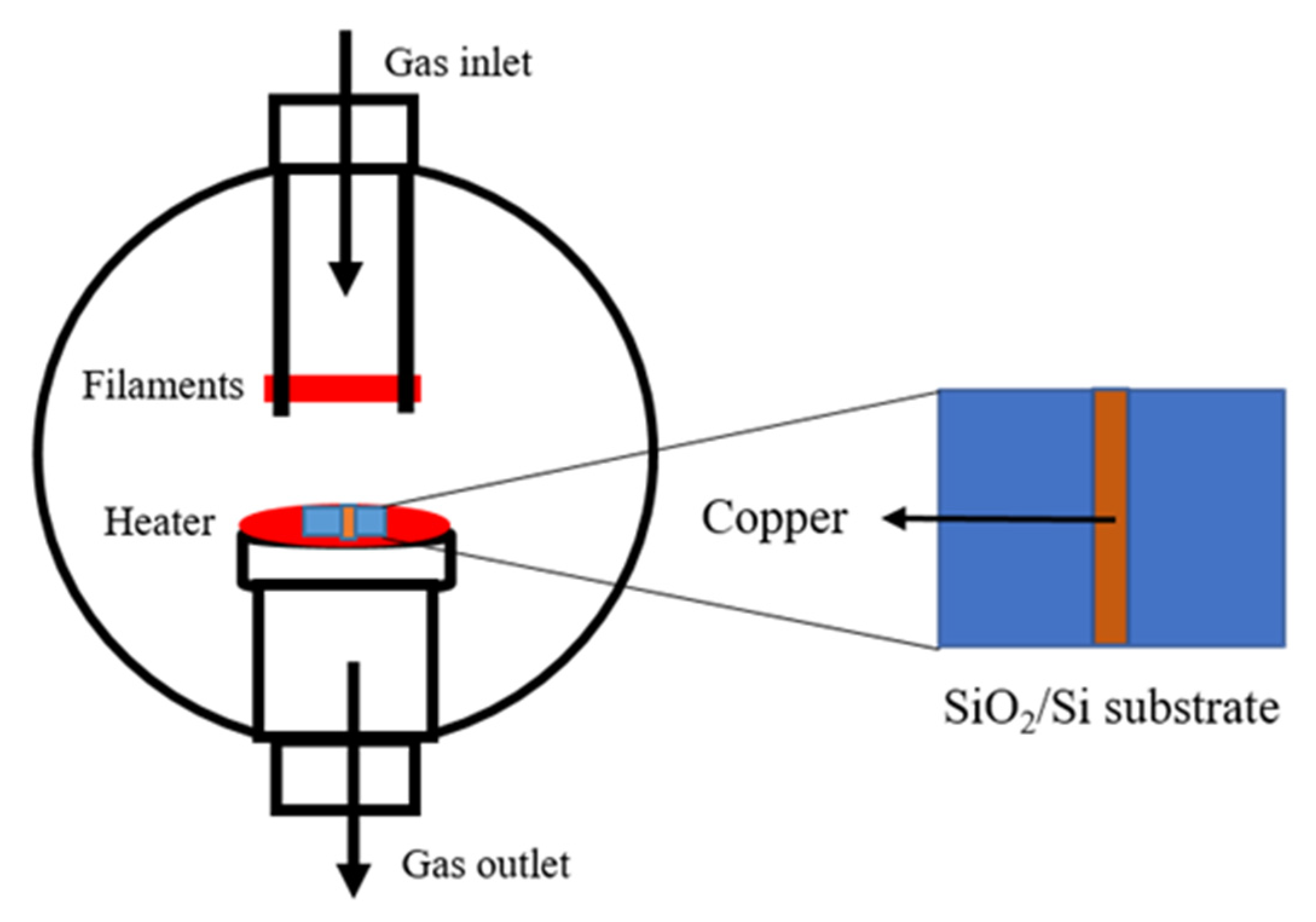
2.1. Substrate Preparation
2.2. Graphene Synthesis
2.3. Characterization
3. Results
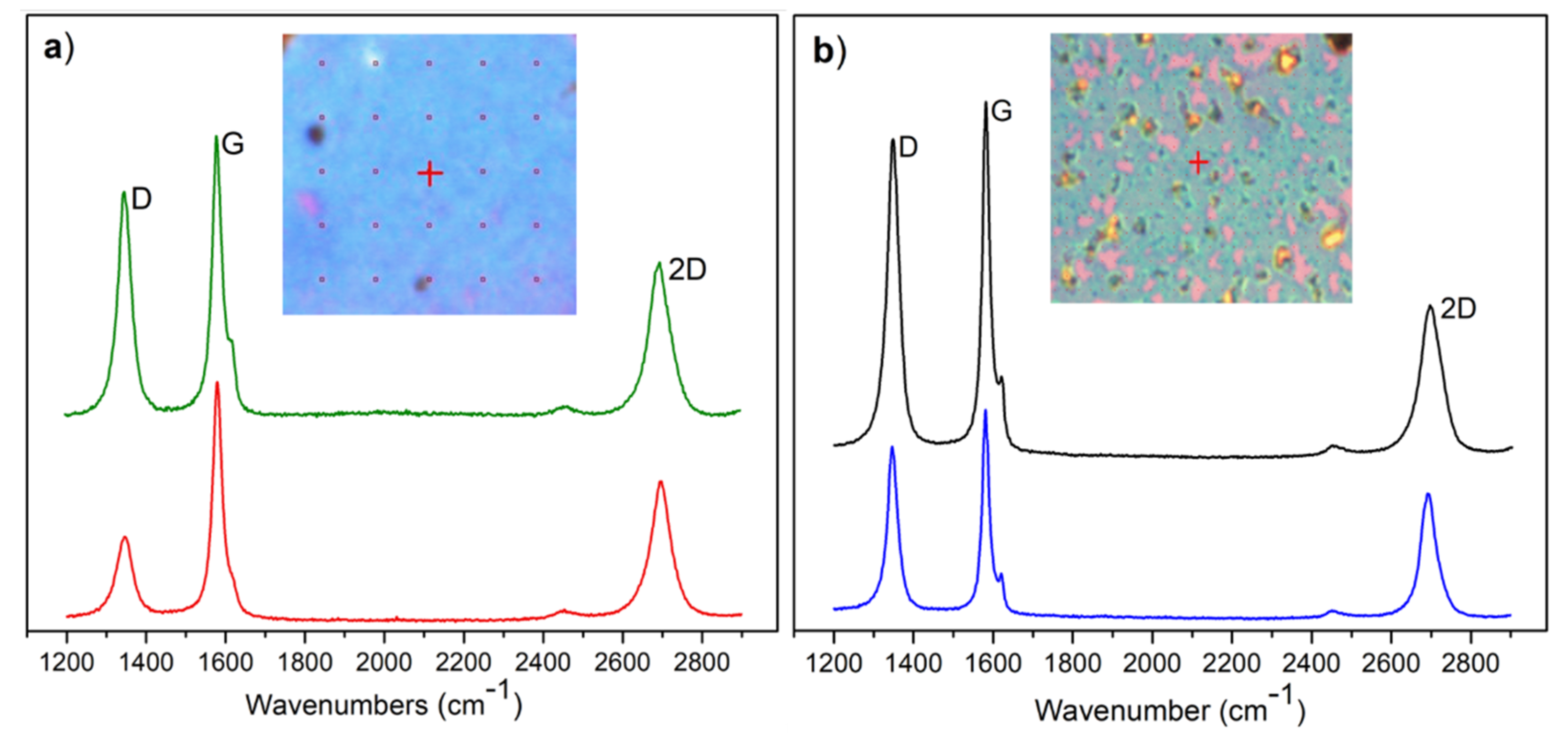
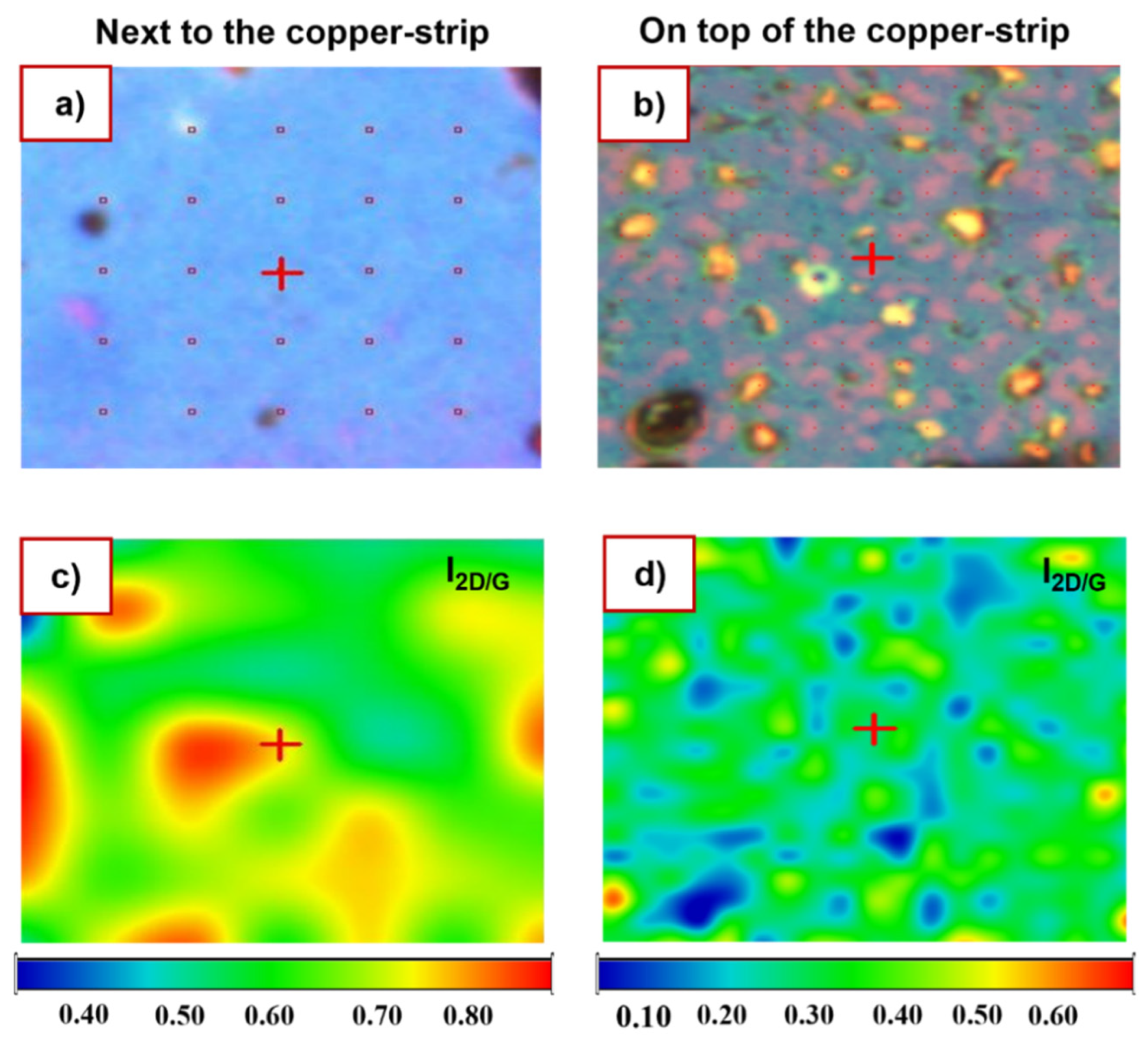
3.1. Raman Analysis
3.2. SEM Analysis
3.3. AFM Analysis
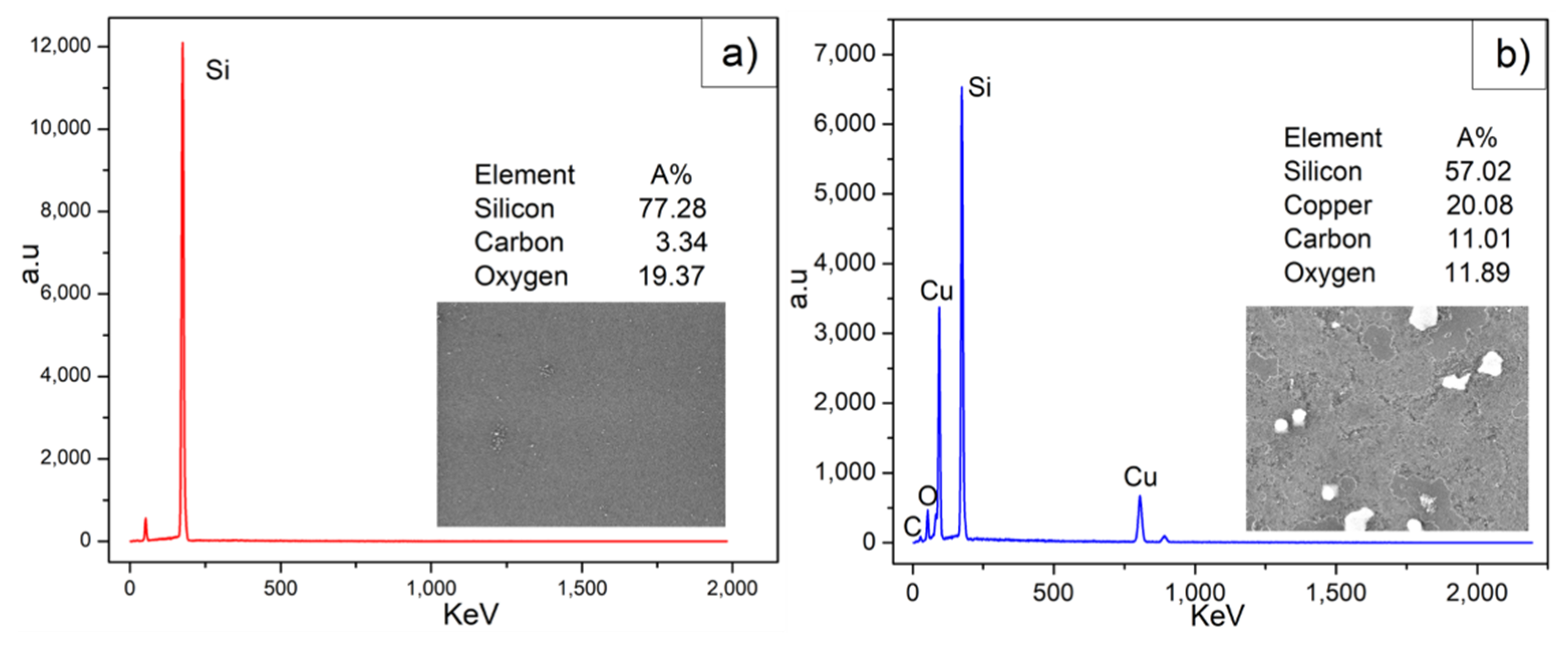
3.4. EDS Analysis
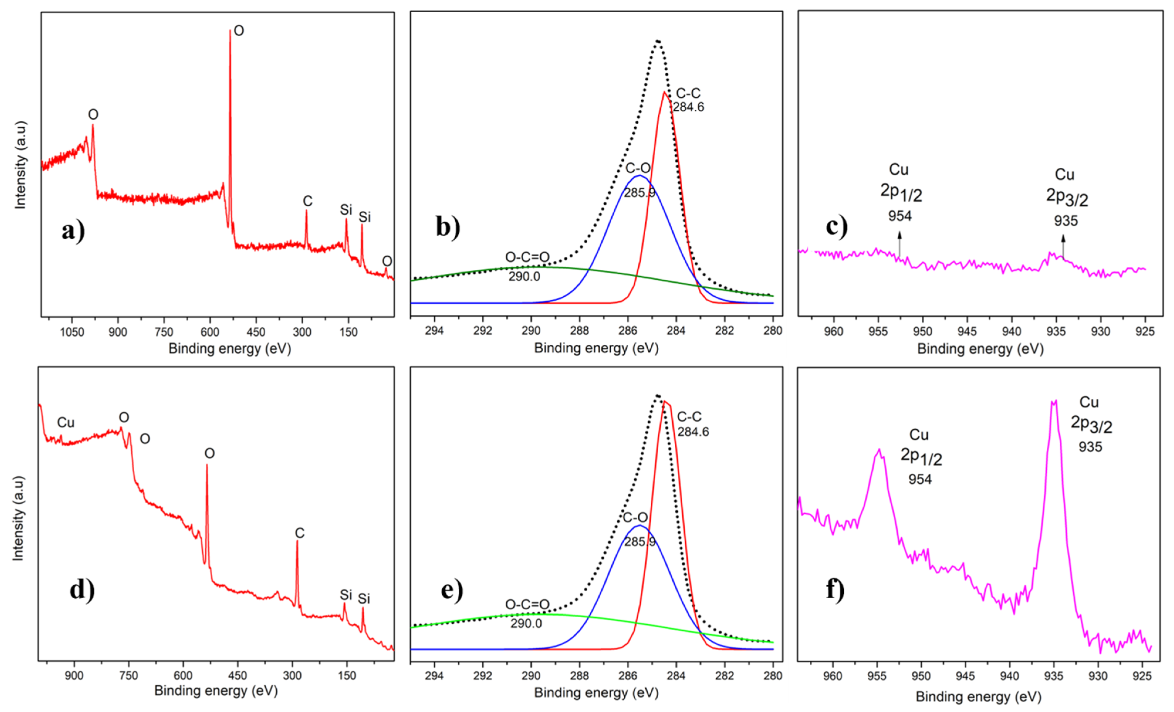
3.5. XPS Analysis
4. Discussion
5. Conclusions
Author Contributions
Funding
Institutional Review Board Statement
Informed Consent Statement
Data Availability Statement
Acknowledgments
Conflicts of Interest
References
- Novoselov, K.; Geim, A.; Morozov, S.; Jiang, D.; Zhang, Y.; Dubonos, S.; Grigorieva, I.; Firsov, A. Electric field in atomically thin carbon films. Science 2004, 306, 666–669. [Google Scholar] [CrossRef] [PubMed] [Green Version]
- De Fazio, D.; Purdie, D.; Ott, A.; Braeuninger-Weimer, P.; Khodkov, T.; Goossens, S.; Taniguchi, T.; Watanabe, K.; Livreri, P.; Koppens, F.; et al. High-mobility, wet-transferred graphene grown by chemical vapor deposition. ACS Nano 2019, 13, 8926–8935. [Google Scholar] [CrossRef] [Green Version]
- Randviir, E.; Brownson, D.; Banks, C. A decade of graphene research: Production, applications and outlook. Mater. Today 2014, 17, 426–432. [Google Scholar] [CrossRef]
- Bunch, J.; van der Zande, A.; Verbridge, S.; Frank, I.; Tanenbaum, D.; Parpia, J.; Craighead, H.; McEuen, P. Electromechanical resonators from graphene sheets. Science 2007, 315, 490–493. [Google Scholar] [CrossRef] [Green Version]
- Raju, A.; Lewis, A.; Derby, B.; Young, R.; Kinloch, I.; Zan, R.; Novoselov, K. Wide-area strain sensors based upon graphene-polymer composite coatings probed by Raman spectroscopy. Adv. Func. Mater. 2014, 24, 2865–2874. [Google Scholar] [CrossRef]
- Kong, W.; Kum, H.; Bae, S.; Shim, J.; Kim, H.; Kong, L.; Meng, Y.; Wang, K.; Kim, C.; Kim, J. Path towards graphene commercialization from lab to market. Nat. Nanotechnol. 2019, 14, 927–938. [Google Scholar] [CrossRef]
- Edwards, R.; Coleman, K. Graphene synthesis: Relationship to applications. Nanoscale 2013, 5, 38–51. [Google Scholar] [CrossRef]
- Bonaccorso, F.; Lombardo, A.; Hasan, T.; Sun, Z.; Colombo, L.; Ferrari, A. Production and processing of graphene and 2D crystals. Mater. Today 2012, 15, 564–589. [Google Scholar] [CrossRef]
- Tan, H.; Wang, D.; Guo, Y. Thermal growth of graphene: A review. Coatings 2018, 8, 40. [Google Scholar] [CrossRef] [Green Version]
- Cooper, D.; D’Anjou, B.; Ghattamaneni, N.; Harack, B.; Hilke, M.; Horth, A.; Majlis, N.; Massicotte, M.; Vandsburger, L.; Whiteway, E.; et al. Experimental review of graphene. Condens. Matter Phys. 2012, 2012, 501686. [Google Scholar] [CrossRef] [Green Version]
- Woehrl, N.; Ochedowski, O.; Gottlieb, S.; Shibasaki, K.; Schulz, S. Plasma-enhanced chemical vapor deposition of graphene on copper substrates. AIP Adv. 2014, 4, 047128. [Google Scholar] [CrossRef] [Green Version]
- Pei, S.; Cheng, H. The reduction of graphene oxide. Carbon 2012, 50, 3210–3228. [Google Scholar] [CrossRef]
- Mishra, N.; Boeckl, J.; Motta, N.; Iacopi, F. Graphene growth on silicon carbide: A review. Phys. Status Solidi A 2016, 213, 2277–2289. [Google Scholar] [CrossRef]
- Reza, G.; Iakimov, T.; Yakimova, R. Epitaxial Graphene on SiC: A Review of Growth and Characterization. Crystals 2016, 6, 53. [Google Scholar]
- Antonova, I. Chemical vapor deposition growth of graphene on copper substrates: Current trends. Phys. Uspekhi 2013, 56, 1013–1020. [Google Scholar] [CrossRef]
- Mattevi, C.; Kima, H.; Chhowalla, M. A review of chemical vapour deposition of graphene on copper. J. Mater. Chem. 2011, 21, 3324–3334. [Google Scholar] [CrossRef]
- Umair, A.; Raza, H. Controlled synthesis of bilayer Graphene on nickel. Nanoscale Res. Lett. 2012, 7, 437. [Google Scholar] [CrossRef] [PubMed] [Green Version]
- Limbu, T.; Hernández, J.; Mendoza, F.; Katiyar, R.; Razink, J.; Makarov, V.; Weiner, B.; Morell, G. A novel approach to the layer-number-controlled and grain-size-controlled growth of high-quality graphene for nanoelectronics. Appl. Nano Mater. 2018, 1, 1502–1512. [Google Scholar] [CrossRef]
- Li, X.; Cai, W.; An, J.; Kim, S.; Nah, J.; Yang, D.; Piner, R.; Velamakanni, A.; Jung, I.; Tutuc, E.; et al. Large-area synthesis of high-quality and uniform graphene films on copper foils. Science 2009, 324, 1312–1314. [Google Scholar] [CrossRef] [PubMed] [Green Version]
- Li, X.; Magnuson, C.; Venugopal, A.; An, J.; Suk, J.; Han, B.; Borysiak, M.; Cai, W.; Velamakanni, A.; Zhu, Y.; et al. Graphene films with large domain size by a two-step chemical vapor deposition process. Nano Lett. 2010, 10, 4328–4334. [Google Scholar] [CrossRef] [Green Version]
- Petrone, N.; Dean, C.; Meric, I.; van der Zande, A.; Huang, P.; Wang, L.; Muller, D.; Shepard, K.; Hone, J. Chemical vapor deposition-derived graphene with electrical performance of exfoliated graphene. Nano Lett. 2012, 12, 2751–2756. [Google Scholar] [CrossRef]
- Mendoza, F.; Limbu, T.; Weiner, B.; Morell, G. Large-area bilayer graphene synthesis in the hot filament chemical vapor deposition reactor. Diam. Relat. Mater. 2015, 51, 34–38. [Google Scholar] [CrossRef]
- Lau, K.; Caulfield, J.; Gleason, K. Structure and morphology of fluorocarbon films grown by hot filament chemical vapor deposition. Chem. Mater. 2000, 12, 3032–3037. [Google Scholar] [CrossRef]
- Hafiz, S.; Chong, S.; Huang, N.; Rahman, S. Fabrication of high-quality graphene by hot-filament thermal chemical vapor deposition. Carbon 2015, 86, 1–11. [Google Scholar] [CrossRef]
- Chen, J.; Wen, Y.; Guo, Y.; Wu, B.; Huang, L.; Xue, Y.; Geng, D.; Wang, D.; Yu, G.; Liu, Y. Oxygen-Aided synthesis of polycrystalline graphene on silicon dioxide substrates. J. Am. Chem. Soc. 2011, 133, 17548–17551. [Google Scholar] [CrossRef] [PubMed]
- Wang, H.; Yu, G. Direct CVD graphene growth on semiconductors and dielectrics for transfer-free device fabrication. Adv. Mater. 2016, 28, 4956–4975. [Google Scholar] [CrossRef]
- Liu, Q.; Gong, Y.; Wang, T.; Chan, W.; Wu, J. Metal-catalyst-free and controllable growth of high-quality monolayer and AB-stacked bilayer graphene on silicon dioxide. Carbon 2016, 96, 203–211. [Google Scholar] [CrossRef] [Green Version]
- Sun, J.; Lindvall, N.; Cole, M.; Wang, T.; Booth, T.; Bøggild, P.; Teo, K.; Liu, J.; Yurgens, A. Controllable chemical vapor deposition of large area uniform nanocrystalline graphene directly on silicon dioxide. Int. J. Appl. Phys. 2012, 111, 044103. [Google Scholar]
- Medina, H.; Lin, Y.; Jin, C.; Lu, C.; Yeh, C.; Huang, K.; Suenaga, K.; Robertson, J.; Chiu, P. Metal-Free Growth of Nanographene on Silicon Oxides for Transparent Conducting Applications. Adv. Funct. Mater. 2012, 22, 2123–2128. [Google Scholar] [CrossRef]
- McNerny, D.; Viswanath, B.; Copic, D.; Laye, F.; Prohoda, C.; Brieland, A.; Polsen, E.; Dee, N.; Veerasamy, V.; Hart, A. Direct fabrication of graphene on SiO2 enabled by thin film stress engineering. Sci. Rep. 2014, 4, 5049. [Google Scholar] [CrossRef] [Green Version]
- Dong, Y.; Xie, Y.; Xu, C.; Li, X.; Deng, J.; Fan, X.; Pan, G.; Wang, Q.; Xiong, F.; Fu, Y.; et al. Transfer-free, lithography-free, and micrometer-precision patterning of CVD graphene on SiO2 toward all-carbon electronics. APL Mater. 2018, 6, 026802. [Google Scholar] [CrossRef] [Green Version]
- Ismach, A.; Druzgalski, C.; Penwell, S.; Schwartzberg, A.; Zheng, M.; Javey, A.; Bokor, J.; Zhang, Y. Direct Chemical Vapor Deposition of Graphene on Dielectric Surfaces. Nano Lett. 2010, 10, 1542–1548. [Google Scholar] [CrossRef]
- Kato, T.; Hatakeyama, R. Direct growth of doping-density controlled hexagonal graphene on SiO2 substrate by rapid-heating plasma CVD. ACS Nano 2012, 6, 8508–8515. [Google Scholar] [CrossRef] [PubMed]
- Zimmer, J.; Ravi, K. Aspects of scaling CVD diamond reactors. Diam. Relat. Mater. 2006, 15, 229–233. [Google Scholar] [CrossRef]
- Ni, Z.; Wang, Y.; Yu, T.; Shen, Z. Raman spectroscopy and imaging of graphene. Nano Res. 2008, 1, 273–291. [Google Scholar] [CrossRef] [Green Version]
- Yang, W.; He, C.; Zhang, L.; Wang, Y.; Shi, Z.; Cheng, M.; Xie, G.; Wang, D.; Yang, R.; Shi, D.; et al. Growth, Characterization, and Properties of Nanographene. Small 2012, 8, 1429–1435. [Google Scholar] [CrossRef]
- Wu, J.; Lin, M.; Cong, X.; Liu, H.; Tan, P. Raman spectroscopy of graphene-based materials and its applications in related devices. Chem. Soc. Rev. 2018, 47, 1822–1873. [Google Scholar] [CrossRef] [PubMed] [Green Version]
- Hawaldar, R.; Merino, P.; Correia, M.; Bdikin, I.; Grácio, J.; Méndez, J.; Martin, J.; Kumar, M. Large-area high-throughput synthesis of monolayer graphene sheet by Hot Filament Thermal Chemical Vapor Deposition. Sci. Rep. 2012, 2, 682. [Google Scholar] [CrossRef] [PubMed] [Green Version]
- Cançado, L.; Takai, K.; Enoki, T. General equation for the determination of the crystallite size La of nanographite by Raman spectroscopy. Appl. Phys. Lett. 2006, 88, 163106. [Google Scholar] [CrossRef]
- Tuinstra, F.; Koenig, J. Raman Spectrum of Graphite. J. Chem. Phys. 1970, 53, 1126. [Google Scholar] [CrossRef] [Green Version]
- Jorio, A.; Ferreira, E.; Moutinho, M.; Stavale, F.; Achete, C.; Capaz, R. Measuring disorder in graphene with the G and D bands. Phys. Status Solidi B 2010, 247, 2980–2982. [Google Scholar] [CrossRef]
- Eckmann, A.; Felten, A.; Mishchenko, A.; Britnell, L.; Krupke, R.; Novoselov, K.; Casiraghi, C. Probing the Nature of Defects in Graphene by Raman Spectroscopy. Nano Lett. 2012, 12, 3925–3930. [Google Scholar] [CrossRef] [Green Version]
- Ferrari, A.; Basko, D. Raman spectroscopy as a versatile tool for studying the properties of graphene. Nat. Nanotechnol. 2013, 8, 235–246. [Google Scholar] [CrossRef] [PubMed] [Green Version]
- Rassapa, S.; Caridad, J.; Schulte, L.; Cagliani, A.; Borah, D.; Morris, M.; Bøggild, P.; Ndoni, S. High quality sub-10 nm graphene nanoribbons by on-chip PS-b-PDMS block copolymer lithography. RSC Adv. 2015, 5, 66711–66717. [Google Scholar] [CrossRef] [Green Version]
- Mikhailov, S. Measuring disorder in graphene with Raman spectroscopy. In Physics and Applications of Graphene—Experiments; InTech Publishers: London, UK, 2011; pp. 439–454. [Google Scholar]
- Reina, A.; Jia, X.; Ho, J.; Nezich, D.; Son, H.; Bulovic, V.; Dresselhaus, M.; Kong, J. Large Area, Few-Layer Graphene Films on Arbitrary Substrates by Chemical Vapor Deposition. Nano Lett. 2009, 9, 30–35. [Google Scholar] [CrossRef] [PubMed]
- Yao, Y.; Ren, L.; Gao, S.; Li, S. Histogram method for reliable thickness measurements of graphene films using atomic force microscopy (AFM). J. Mater. Sci. Technol. 2017, 33, 815–820. [Google Scholar] [CrossRef]
- Nemes-Incze, P.; Osvatha, Z.; Kamaras, K.; Biro, L. Anomalies in thickness measurements of graphene and few layer graphite crystals by tapping mode atomic force microscopy. Carbon 2008, 46, 1435–1442. [Google Scholar] [CrossRef] [Green Version]
- Ferrah, D.; Penuelas, J.; Bottela, C.; Grenet, G.; Ouerghi, A. X-ray photoelectron spectroscopy (XPS) and diffraction (XPD) study of a few layers of graphene on 6H-SiC (0001). Surf. Sci. 2013, 615, 47–56. [Google Scholar] [CrossRef]
- Moulder, J. Handbook of X-Ray Photoelectron Spectroscopy; Physical Electronics Division, Perkin-Elmer Corporation: Eden Prairie, MN, USA, 1992. [Google Scholar]
- Teng, P.; Lu, C.; Akiyama, K.; Lin, Y.; Yeh, C.; Suenaga, K.; Chiu, P. Remote Catalyzation for Direct Formation of Graphene Layers on Oxides. Nano Lett. 2012, 12, 1379–1384. [Google Scholar] [CrossRef]
- Song, Y.; Liu, J.; Quan, L.; Pan, N.; Zhu, H.; Wang, X. Size Dependence of Compressive Strain in Graphene Flakes Directly Grown on SiO2/Si Substrate. J. Phys. Chem. C 2014, 118, 12526–12531. [Google Scholar] [CrossRef]
- Kim, H.; Song, I.; Park, C.; Son, M.; Hong, M.; Kim, Y.; Kim, J.; Shin, H.; Baik, J.; Choi, H. Copper Vapor-Assisted Direct Growth of High Quality and Metal-Free Single Layer Graphene on Amorphous SiO2 Substrate. ACS Nano 2013, 7, 6575–6582. [Google Scholar] [CrossRef] [PubMed]
- Luo, B.; Caridad, J.; Whelan, P.; Thomsen, J.; Mackenzie, D.; Cabo, A.; Mahatha, S.; Bianchi, M.; Hofmann, P.; Jepsen, P.; et al. Sputtering an exterior metal coating on copper enclosure for large-scale growth of single-crystalline graphene. 2D Mater. 2017, 4, 045017. [Google Scholar] [CrossRef]
- Muñoz, R.; Gómez, C. Review of CVD synthesis of graphene. Chem. Vap. Depos. 2013, 19, 297–322. [Google Scholar] [CrossRef] [Green Version]
- Bhaviripudi, S.; Jia, X.; Dresselhaus, M.; Kong, J. Role of kinetic factors in chemical vapor deposition synthesis of uniform large area graphene using copper catalyst. Nano Lett. 2010, 10, 4128–4133. [Google Scholar] [CrossRef] [PubMed]


| Method | CVD Type | Substrate | Pre-Growth Step | Carbon Source/ Temperature | References |
|---|---|---|---|---|---|
| Catalyst-free | Tube Furnace | SiO2 (0, 90, 300, 500 nm)/Si | H2 (70–160 sccm)/1060–1100 °C | CH4 (30 sccm)/1060–1100 °C | [27] |
| SiO2 (300 nm)/Si | H2 (50 sccm) and Ar (1000 sccm)/1000 °C | CH4 (300 sccm)/1000 °C | [28] | ||
| ECR plasma | SiO2/Si, quartz, and glass | Ar (5sccm)/400 °C | C2H4 (0.12 sccm) and Ar (0.12 sccm)/400 °C | [29] | |
| Metal-catalyzed | Tube Furnace | Ni layer/silicon | H2 or He (400sccm)/ 900 °C | CH4 or C2H2 (50 sccm) and H2 (50 sccm)/900 °C | [30] |
| Cu layer (60 nm)/SiO2 (300 nm)/Si | H2 (35 sccm)/1000 °C | CH4 (30 sccm) and H2 (20 sccm)/960 °C | [31] | ||
| Cu layer (450 to 100 nm)/quartz, sapphire, SiO2 (300 nm)/Si, and fused silica | H2 (35 sccm)/1000 °C | CH4 (35 sccm) and H2 (2 sccm)/1000 °C | [32] | ||
| Rapid heating plasma | Ni film (55 nm)/SiO2 (300 nm)/Si | CH4:H2 (9:1)/600–975 °C | CH4:H2 (9:1)/950 °C | [33] |
Publisher’s Note: MDPI stays neutral with regard to jurisdictional claims in published maps and institutional affiliations. |
© 2021 by the authors. Licensee MDPI, Basel, Switzerland. This article is an open access article distributed under the terms and conditions of the Creative Commons Attribution (CC BY) license (https://creativecommons.org/licenses/by/4.0/).
Share and Cite
Rodríguez-Villanueva, S.; Mendoza, F.; Instan, A.A.; Katiyar, R.S.; Weiner, B.R.; Morell, G. Graphene Growth Directly on SiO2/Si by Hot Filament Chemical Vapor Deposition. Nanomaterials 2022, 12, 109. https://doi.org/10.3390/nano12010109
Rodríguez-Villanueva S, Mendoza F, Instan AA, Katiyar RS, Weiner BR, Morell G. Graphene Growth Directly on SiO2/Si by Hot Filament Chemical Vapor Deposition. Nanomaterials. 2022; 12(1):109. https://doi.org/10.3390/nano12010109
Chicago/Turabian StyleRodríguez-Villanueva, Sandra, Frank Mendoza, Alvaro A. Instan, Ram S. Katiyar, Brad R. Weiner, and Gerardo Morell. 2022. "Graphene Growth Directly on SiO2/Si by Hot Filament Chemical Vapor Deposition" Nanomaterials 12, no. 1: 109. https://doi.org/10.3390/nano12010109
APA StyleRodríguez-Villanueva, S., Mendoza, F., Instan, A. A., Katiyar, R. S., Weiner, B. R., & Morell, G. (2022). Graphene Growth Directly on SiO2/Si by Hot Filament Chemical Vapor Deposition. Nanomaterials, 12(1), 109. https://doi.org/10.3390/nano12010109