
Selective Area Epitaxy of GaN Nanowires on Si Substrates Using Microsphere Lithography: Experiment and Theory

 ,
,  , , ,
, , , 
Abstract
:1. Introduction
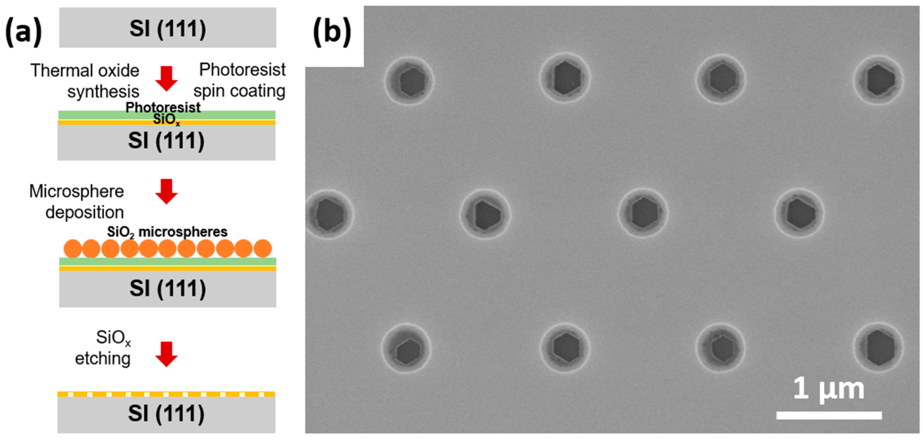
2. Experimental
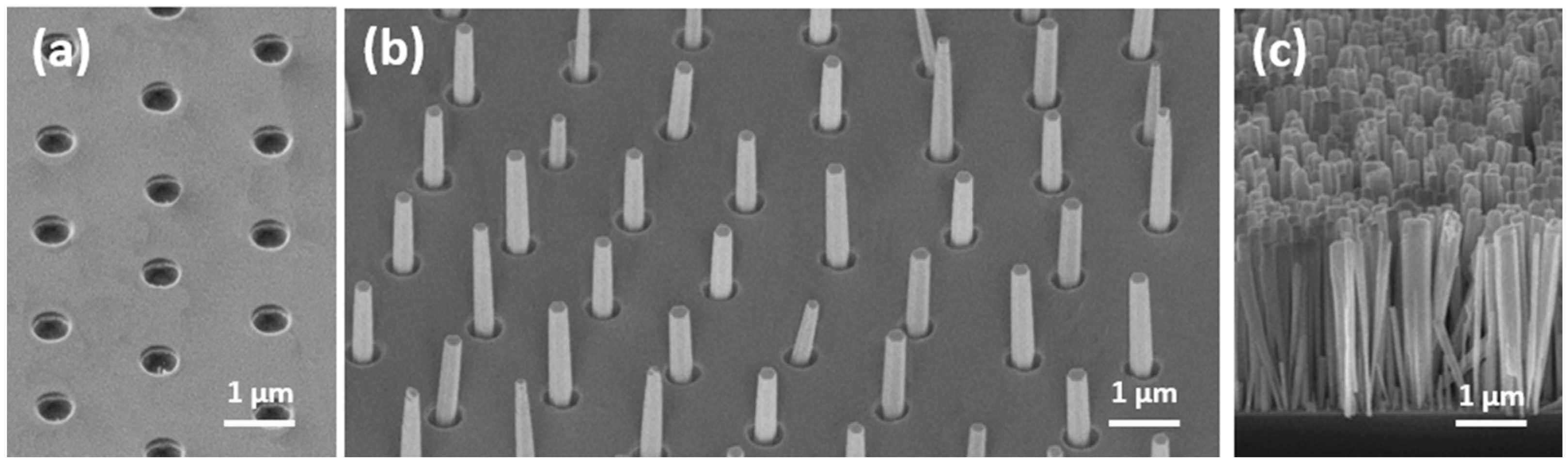
3. Results and Discussion
3.1. Influence of the MBE Growth Conditions on the NW Morphology
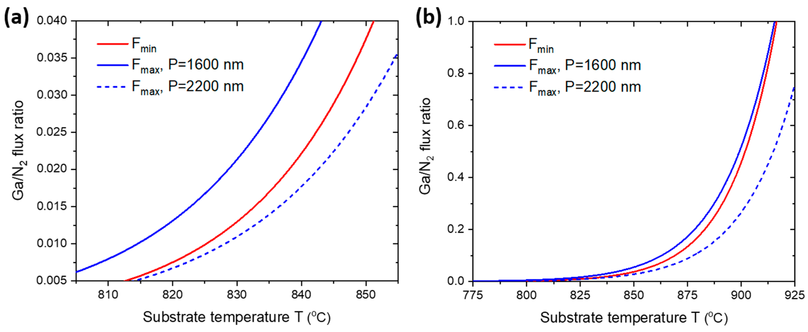
3.2. Model
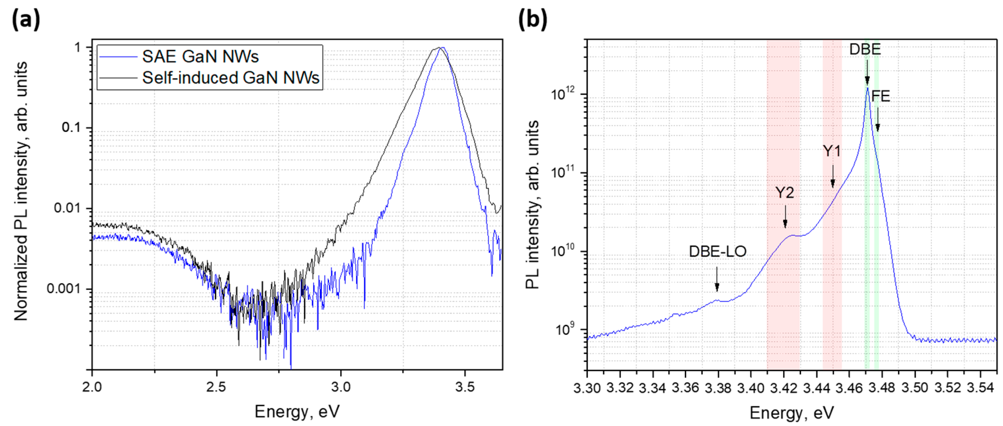
3.3. Optical Studies
4. Conclusions
Author Contributions
Funding
Data Availability Statement
Conflicts of Interest
References
- Holmes, M.J.; Choi, K.; Kako, S.; Arita, M.; Arakawa, Y. Room-Temperature Triggered Single Photon Emission from a III-Nitride Site-Controlled Nanowire Quantum Dot. Nano Lett. 2014, 14, 982–986. [Google Scholar] [CrossRef] [PubMed]
- Wright, J.B.; Liu, S.; Wang, G.T.; Li, Q.; Benz, A.; Koleske, D.D.; Lu, P.; Xu, H.; Lester, L.; Luk, T.S. Multi-Colour Nanowire Photonic Crystal Laser Pixels. Sci. Rep. 2013, 3, 2982. [Google Scholar] [CrossRef] [PubMed] [Green Version]
- Ra, Y.-H.; Lee, C.-R. Ultracompact Display Pixels: Tunnel Junction Nanowire Photonic Crystal Laser. Nano Energy 2021, 84, 105870. [Google Scholar] [CrossRef]
- Dvoretckaia, L.; Gridchin, V.; Mozharov, A.; Maksimova, A.; Dragunova, A.; Melnichenko, I.; Mitin, D.; Vinogradov, A.; Mukhin, I.; Cirlin, G. Light-Emitting Diodes Based on InGaN/GaN Nanowires on Microsphere-Lithography-Patterned Si Substrates. Nanomaterials 2022, 12, 1993. [Google Scholar] [CrossRef] [PubMed]
- Dubrovskii, V.; Cirlin, G.; Ustinov, V. Semiconductor Nanowhiskers: Synthesis, Properties, and Applications. Semiconductors 2009, 43, 1539–1584. [Google Scholar] [CrossRef]
- Tchernycheva, M.; Sartel, C.; Cirlin, G.; Travers, L.; Patriarche, G.; Harmand, J.; Dang, L.S.; Renard, J.; Gayral, B.; Nevou, L. Growth of GaN Free-Standing Nanowires by Plasma-Assisted Molecular Beam Epitaxy: Structural and Optical Characterization. Nanotechnology 2007, 18, 385306. [Google Scholar] [CrossRef]
- Xu, Z.; Zhang, L.; He, H.; Wang, J.; Xie, M. Growth of GaN on Si (111): Surfaces and Crystallinity of the Epifilms and the Transport Behavior of GaN/Si Heterojunctions. J. Appl. Phys. 2011, 110, 093514. [Google Scholar] [CrossRef] [Green Version]
- Alias, M.S.; Tangi, M.; Holguin-Lerma, J.A.; Stegenburgs, E.; Alatawi, A.A.; Ashry, I.; Subedi, R.C.; Priante, D.; Shakfa, M.K.; Ng, T.K. Review of Nanophotonics Approaches Using Nanostructures and Nanofabrication for III-Nitrides Ultraviolet-Photonic Devices. J. Nanophotonics 2018, 12, 043508. [Google Scholar] [CrossRef]
- Zhao, C.; Alfaraj, N.; Subedi, R.C.; Liang, J.W.; Alatawi, A.A.; Alhamoud, A.A.; Ebaid, M.; Alias, M.S.; Ng, T.K.; Ooi, B.S. III-Nitride Nanowires on Unconventional Substrates: From Materials to Optoelectronic Device Applications. Prog. Quantum Electron. 2018, 61, 1–31. [Google Scholar] [CrossRef]
- Akopian, N.; Lindner, N.; Poem, E.; Berlatzky, Y.; Avron, J.; Gershoni, D.; Gerardot, B.; Petroff, P. Entangled Photon Pairs from Semiconductor Quantum Dots. Phys. Rev. Lett. 2006, 96, 130501. [Google Scholar] [CrossRef] [Green Version]
- Peřina, J., Jr.; Centini, M.; Sibilia, C.; Bertolotti, M.; Scalora, M. Antisymmetric Entangled Two-Photon States Generated in Nonlinear Ga N/Al N Photonic-Band-Gap Structures. Phys. Rev. A 2007, 75, 013805. [Google Scholar] [CrossRef]
- Patra, S.K.; Schulz, S. Indium Gallium Nitride Quantum Dots: Consequence of Random Alloy Fluctuations for Polarization Entangled Photon Emission. Mater. Quantum Technol. 2020, 1, 015001. [Google Scholar] [CrossRef]
- Motayed, A.; Vaudin, M.; Davydov, A.V.; Melngailis, J.; He, M.; Mohammad, S. Diameter Dependent Transport Properties of Gallium Nitride Nanowire Field Effect Transistors. Appl. Phys. Lett. 2007, 90, 043104. [Google Scholar] [CrossRef]
- Sekiguchi, H.; Kishino, K.; Kikuchi, A. Emission Color Control from Blue to Red with Nanocolumn Diameter of InGaN/GaN Nanocolumn Arrays Grown on Same Substrate. Appl. Phys. Lett. 2010, 96, 231104. [Google Scholar] [CrossRef]
- Leng, H.; Yu, X.; Gong, Y.; Xu, P.; Xie, Z.; Jin, H.; Zhang, C.; Zhu, S. On-Chip Steering of Entangled Photons in Nonlinear Photonic Crystals. Nat. Commun. 2011, 2, 429. [Google Scholar] [CrossRef] [Green Version]
- Takeuchi, S. Recent Progress in Single-Photon and Entangled-Photon Generation and Applications. Jpn. J. Appl. Phys. 2014, 53, 030101. [Google Scholar] [CrossRef]
- Gotschke, T.; Schumann, T.; Limbach, F.; Stoica, T.; Calarco, R. Influence of the Adatom Diffusion on Selective Growth of GaN Nanowire Regular Arrays. Appl. Phys. Lett. 2011, 98, 103102. [Google Scholar] [CrossRef] [Green Version]
- Kruse, J.; Lymperakis, L.; Eftychis, S.; Adikimenakis, A.; Doundoulakis, G.; Tsagaraki, K.; Androulidaki, M.; Olziersky, A.; Dimitrakis, P.; Ioannou-Sougleridis, V. Selective-Area Growth of GaN Nanowires on SiO2-Masked Si (111) Substrates by Molecular Beam Epitaxy. J. Appl. Phys. 2016, 119, 224305. [Google Scholar] [CrossRef]
- Kishino, K.; Ishizawa, S. Selective-Area Growth of GaN Nanocolumns on Si (111) Substrates for Application to Nanocolumn Emitters with Systematic Analysis of Dislocation Filtering Effect of Nanocolumns. Nanotechnology 2015, 26, 225602. [Google Scholar] [CrossRef]
- Li, G.; Yao, Y.; Dagenais, M. Selective Area Growth of GaN Nanowires on Si (1 1 1) Substrate with Ti Masks by Molecular Beam Epitaxy. J. Cryst. Growth 2019, 524, 125181. [Google Scholar] [CrossRef]
- Schuster, F.; Hetzl, M.; Weiszer, S.; Garrido, J.A.; De La Mata, M.; Magen, C.; Arbiol, J.; Stutzmann, M. Position-Controlled Growth of GaN Nanowires and Nanotubes on Diamond by Molecular Beam Epitaxy. Nano Lett. 2015, 15, 1773–1779. [Google Scholar] [CrossRef] [PubMed] [Green Version]
- Sekiguchi, H.; Higashi, Y.; Yamane, K.; Wakahara, A.; Okada, H.; Kishino, K. Fabrication and Optical Properties of Regularly Arranged GaN-Based Nanocolumns on Si Substrate. J. Vac. Sci. Technol. B Nanotechnol. Microelectron. Mater. Process. Meas. Phenom. 2019, 37, 031207. [Google Scholar] [CrossRef]
- Bengoechea-Encabo, A.; Barbagini, F.; Fernandez-Garrido, S.; Grandal, J.; Ristic, J.; Sanchez-Garcia, M.A.; Calleja, E.; Jahn, U.; Luna, E.; Trampert, A. Understanding the Selective Area Growth of GaN Nanocolumns by MBE Using Ti Nanomasks. J. Cryst. Growth 2011, 325, 89–92. [Google Scholar] [CrossRef] [Green Version]
- Zhang, Z.; Geng, C.; Hao, Z.; Wei, T.; Yan, Q. Recent Advancement on Micro-/Nano-Spherical Lens Photolithography Based on Monolayer Colloidal Crystals. Adv. Colloid Interface Sci. 2016, 228, 105–122. [Google Scholar] [CrossRef] [Green Version]
- Dvoretckaia, L.N.; Mozharov, A.M.; Berdnikov, Y.; Mukhin, I.S. Optimization of Microsphere Optical Lithography for Nano-Patterning. J. Phys. D Appl. Phys. 2021, 55, 09LT01. [Google Scholar] [CrossRef]
- García Núñez, C.; Navaraj, W.T.; Liu, F.; Shakthivel, D.; Dahiya, R. Large-Area Self-Assembly of Silica Microspheres/Nanospheres by Temperature-Assisted Dip-Coating. ACS Appl. Mater. Interfaces 2018, 10, 3058–3068. [Google Scholar] [CrossRef]
- Zhu, J.; Goddard, L.L. Spatial Control of Photonic Nanojets. Opt. Express 2016, 24, 30444–30464. [Google Scholar] [CrossRef]
- Gridchin, V.O.; Kotlyar, K.P.; Reznik, R.R.; Dragunova, A.S.; Kryzhanovskaya, N.V.; Lendyashova, V.V.; Kirilenko, D.A.; Soshnikov, I.P.; Shevchuk, D.S.; Cirlin, G.G. Multi-Colour Light Emission from InGaN Nanowires Monolithically Grown on Si Substrate by MBE. Nanotechnology 2021, 32, 335604. [Google Scholar] [CrossRef]
- Robson, M.; Dubrovskii, V.; LaPierre, R. Conditions for High Yield of Selective-Area Epitaxy InAs Nanowires on SiOx/Si (111) Substrates. Nanotechnology 2015, 26, 465301. [Google Scholar] [CrossRef]
- Dubrovskii, V. Gallium Diffusion Flow Direction during Deposition on the Surface with Regular Hole Arrays. Tech. Phys. Lett. 2021, 47, 601–604. [Google Scholar] [CrossRef]
- Sobanska, M.; Dubrovskii, V.; Tchutchulashvili, G.; Klosek, K.; Zytkiewicz, Z. Analysis of Incubation Times for the Self-Induced Formation of GaN Nanowires: Influence of the Substrate on the Nucleation Mechanism. Cryst. Growth Des. 2016, 16, 7205–7211. [Google Scholar] [CrossRef]
- Consonni, V.; Dubrovskii, V.; Trampert, A.; Geelhaar, L.; Riechert, H. Quantitative Description for the Growth Rate of Self-Induced GaN Nanowires. Phys. Rev. B 2012, 85, 155313. [Google Scholar] [CrossRef] [Green Version]
- Dubrovskii, V.G. Theory of VLS Growth of Compound Semiconductors. In Semiconductors and Semimetals; Elsevier: Amsterdam, The Netherlands, 2015; Volume 93, pp. 1–78. ISBN 0080-8784. [Google Scholar]
- Reshchikov, M.A. Measurement and Analysis of Photoluminescence in GaN. J. Appl. Phys. 2021, 129, 121101. [Google Scholar] [CrossRef]
- Reshchikov, M.A. Evaluation of GaN by Photoluminescence Measurement. Phys. Status Solidi 2011, 8, 2136–2138. [Google Scholar] [CrossRef]
- Reshchikov, M.A.; Morkoç, H. Luminescence Properties of Defects in GaN. J. Appl. Phys. 2005, 97, 061301. [Google Scholar] [CrossRef]
- Brandt, O.; Pfüller, C.; Chèze, C.; Geelhaar, L.; Riechert, H. Sub-MeV Linewidth of Excitonic Luminescence in Single GaN Nanowires: Direct Evidence for Surface Excitons. Phys. Rev. B 2010, 81, 045302. [Google Scholar] [CrossRef] [Green Version]
- Van Nostrand, J.; Averett, K.; Cortez, R.; Boeckl, J.; Stutz, C.; Sanford, N.A.; Davydov, A.; Albrecht, J. Molecular Beam Epitaxial Growth of High-Quality GaN Nanocolumns. J. Cryst. Growth 2006, 287, 500–503. [Google Scholar] [CrossRef]
- Schuster, F.; Furtmayr, F.; Zamani, R.; Magén, C.; Morante, J.R.; Arbiol, J.; Garrido, J.A.; Stutzmann, M. Self-Assembled GaN Nanowires on Diamond. Nano Lett. 2012, 12, 2199–2204. [Google Scholar] [CrossRef]
- Albert, S.; Bengoechea-Encabo, A.; Sanchez-Garcia, M.; Barbagini, F.; Calleja, E.; Luna, E.; Trampert, A.; Jahn, U.; Lefebvre, P.; Lopez, L. Efficient Phosphor-Free, White Light Emission by Using Ordered Arrays of GaN/InGaN Nanocolumnar LEDs Grown by Selective Area MBE; World Scientific Publishing: Singapore, 2011; Volume 21, p. 1250010. [Google Scholar]
- Kumaresan, V.; Largeau, L.; Oehler, F.; Zhang, H.; Mauguin, O.; Glas, F.; Gogneau, N.; Tchernycheva, M.; Harmand, J. Self-Induced Growth of Vertical GaN Nanowires on Silica. Nanotechnology 2016, 27, 135602. [Google Scholar] [CrossRef]
- Auzelle, T.; Haas, B.; Den Hertog, M.; Rouvière, J.-L.; Daudin, B.; Gayral, B. Attribution of the 3.45 EV GaN Nanowires Luminescence to Inversion Domain Boundaries. Appl. Phys. Lett. 2015, 107, 051904. [Google Scholar] [CrossRef]
- Sam-Giao, D.; Mata, R.; Tourbot, G.; Renard, J.; Wysmolek, A.; Daudin, B.; Gayral, B. Fine Optical Spectroscopy of the 3.45 EV Emission Line in GaN Nanowires. J. Appl. Phys. 2013, 113, 043102. [Google Scholar] [CrossRef] [Green Version]
- Yi, S.; Na, J.H.; Lee, K.H.; Jarjour, A.F.; Taylor, R.A.; Park, Y.; Kang, T.; Kim, S.; Ha, D.; Andrew, G. Photoluminescence Properties of a Single GaN Nanorod with Ga N/Al Ga N Multilayer Quantum Disks. Appl. Phys. Lett. 2007, 90, 101901. [Google Scholar] [CrossRef] [Green Version]

Publisher’s Note: MDPI stays neutral with regard to jurisdictional claims in published maps and institutional affiliations. |
© 2022 by the authors. Licensee MDPI, Basel, Switzerland. This article is an open access article distributed under the terms and conditions of the Creative Commons Attribution (CC BY) license (https://creativecommons.org/licenses/by/4.0/).
Share and Cite
Gridchin, V.O.; Dvoretckaia, L.N.; Kotlyar, K.P.; Reznik, R.R.; Parfeneva, A.V.; Dragunova, A.S.; Kryzhanovskaya, N.V.; Dubrovskii, V.G.; Cirlin, G.E. Selective Area Epitaxy of GaN Nanowires on Si Substrates Using Microsphere Lithography: Experiment and Theory. Nanomaterials 2022, 12, 2341. https://doi.org/10.3390/nano12142341
Gridchin VO, Dvoretckaia LN, Kotlyar KP, Reznik RR, Parfeneva AV, Dragunova AS, Kryzhanovskaya NV, Dubrovskii VG, Cirlin GE. Selective Area Epitaxy of GaN Nanowires on Si Substrates Using Microsphere Lithography: Experiment and Theory. Nanomaterials. 2022; 12(14):2341. https://doi.org/10.3390/nano12142341
Chicago/Turabian StyleGridchin, Vladislav O., Liliia N. Dvoretckaia, Konstantin P. Kotlyar, Rodion R. Reznik, Alesya V. Parfeneva, Anna S. Dragunova, Natalia V. Kryzhanovskaya, Vladimir G. Dubrovskii, and George E. Cirlin. 2022. "Selective Area Epitaxy of GaN Nanowires on Si Substrates Using Microsphere Lithography: Experiment and Theory" Nanomaterials 12, no. 14: 2341. https://doi.org/10.3390/nano12142341