Abstract
In situ MgB2 superconducting samples were prepared by using the spark plasma sintering method. The density of the obtained bulks was up to 95% of the theoretical value predicted for the material. The structural and microstructural characterizations of the samples were investigated using X-ray diffraction and SEM and correlated to their superconducting properties, in particular their critical current densities, Jc, which was measured at 20 K. Extremely high critical current densities of up to 6.75 × 10⁵ A/cm2 in the self-field and above 104 A/cm2 at 4 T were measured at 20 K, indicating that vortex pinning is very strong. This property is mainly attributed to the sample density and MgB2 nanograins in connection to the presence of MgO precipitates and areas rich in boron.
1. Introduction
MgB2 is an intermetallic superconductor [1]. The superconductivity of this material was reported for the first time in 2001 [2]. This compound has excellent superconducting properties, especially its high critical current density [3,4] and trapped magnetic field [5], due to a strong pinning of the vortices. The voids, disorders and impurities present in the material can behave as pinning centers that hamper the vortex motion and minimize energy dissipation. Unlike cuprate superconductors [6,7], the Jc values of MgB2 can be strongly enhanced by increasing the number of grain boundaries while decreasing the grains’ size [8,9]. Although its transition temperature is relatively low for many applications (39 K), the processing conditions of MgB2-based materials are simpler and much cheaper than those of the cuprate superconductors. Otherwise, for applications, costs can be saved by using cryo-coolers apparatus above 4 K or developing technologies that use liquid hydrogen as a cooling fluid [10]. To prepare highly dense MgB2 bulk superconductors, spark plasma sintering (SPS) is a very interesting technique [11,12]. It is a rapid consolidation method that results in a good understanding and control of the sintering kinetics, as reported elsewhere [11]. The heat source is not external but is an electric current (AC, DC or pulsed) that flows across the die containing the powder to sinter. Simultaneously, a uni-axial pressure is applied. The main difference between SPS and conventional or hot-pressing methods is that SPS allows for the preparation of highly dense samples with grain growth control and a decreased processing time [13,14,15,16]. Concerning MgB2, the samples processed by SPS additionally show excellent mechanical properties [17].
In this contribution, we report the remarkable superconducting properties of MgB2 samples containing nanoparticles densified by SPS, especially their very high critical current density, Jc.
2. Experimental Section
Two samples, namely sample A and sample R, were fabricated using the same sintering conditions. The aim was to investigate the sample reproducibility. The starting powders used to prepare the samples were Mg metal (99.8%, 325 mesh, Alfa Aesar, Haverhillm, MA, USA) and amorphous B powder (99%, <400 nm, PAVEZYUM advanced Chemicals, Dilovası, Turkey), mixed at the molar ratio of 1:2. A total of 1.5 g of starting powder was weighed and loaded into a tungsten carbide (WC) mold (20 mm diameter). Graphite foils were wrapped alongside the inner wall of the mold and inserted between the powder and two punches to facilitate demolding. The mold can be reused if employed within some temperature and pressure limits, usually under 850 °C and 500 MPa. The samples were sintered by spark plasma sintering (FCT Systeme GmbH, HD25, Rauenstein, Thuringia, Germany) in DC mode under dynamic vacuum (10−3 bar) with the following protocol:
- (i)
- 500 °C + 260 MPa/15 min (Powder compaction);
- (ii)
- 650 °C + 280 MPa/20 min (Synthesis);
- (iii)
- 750 °C + 300 MPa/30 min (Sintering/Densification).
The introduction of these different steps aimed at avoiding magnesium evaporation. The heating rate was 100 °C/min, and the cooling time was about 20 min. The total processing duration was approximately 100 min. With respect to conventional graphite molds [11,12], WC molds sustain a higher pressure, allowing for a lower processing temperature and better control of the grain size. The bulks were polished before characterization. The density of the samples was measured using the Archimedes method with ethanol [18]. The crystalline phases present in the samples were analyzed by X-ray diffraction (XRD) with a Philips θ–2θ diffractometer and the monochromatic Cu-Kα radiation. The microstructure was analyzed with a scanning electron microscope (SEM, JEOL 7200, Tokyo, Japan). Small specimens with dimensions of 1.51 × 1.54 × 1.62 and 1.48 × 1.45 × 1.84 mm3 were cut from the two fabricated, bulks A and R, to investigate their superconducting properties with a SQUID magnetometer (Quantum Design, model MPMS, San Diego, CA, USA). The magnetic moment was firstly measured from 20 K to 40 K with an applied field of 20 Oe in order to determine the critical temperature; then, they were measured at various temperatures as a function of the applied field. The critical current density, Jc was deduced from the resulting hysteresis loops using the extended Bean model equation [19] for samples with rectangular sections:
where a and b (a ≤ b) are the width and length of the specimens, and c is their thickness. ∆M is the difference in magnetization between increasing and decreasing magnetic fields. A small parallelepiped sample with dimensions of 1.47 × 1.67 × 9.8 mm3 was cut from sample A; then, the electrical resistivity was measured using a DC 4-probe method with a PPMS (Quantum Design, San Diego, CA, USA) system. The contacts on the samples were made using silver paste. The current applied to the bar sample was 5 mA. The resistance was measured as a function of the temperature (10–300 K, sweep mode) while applying a magnetic field of up to 14 T.
Jc = 20∆M/[a2c (b − a/3)]
3. Results and Discussion
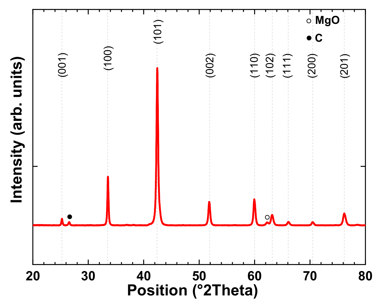
The samples A and R showed the same properties. Their density was 2.46 g/cm3, corresponding to 95% of the theoretical value. The XRD of sample A reported in Figure 1 shows that the major peaks were due to the MgB2 phase with traces of MgO (3 wt.%, evaluated by the Maud refinement, [20]). The presence of MgO could be related either to the oxidation of Mg during the sintering process or to a redox reaction between B2O3 and Mg [21]. The B2O3 phase was already present in the boron powder and could react with Mg due to its low melting point (≈450 °C). Small peaks of residual carbon due to the residual carbon foil were also observed [16]. The MgB2 crystallite size as estimated from Rietveld refinement (isotropic size–strain model of Maud [22]) was 58 0.6 nm, supposing a Gaussian distribution.

Figure 1.
X-ray diagram of sample A.
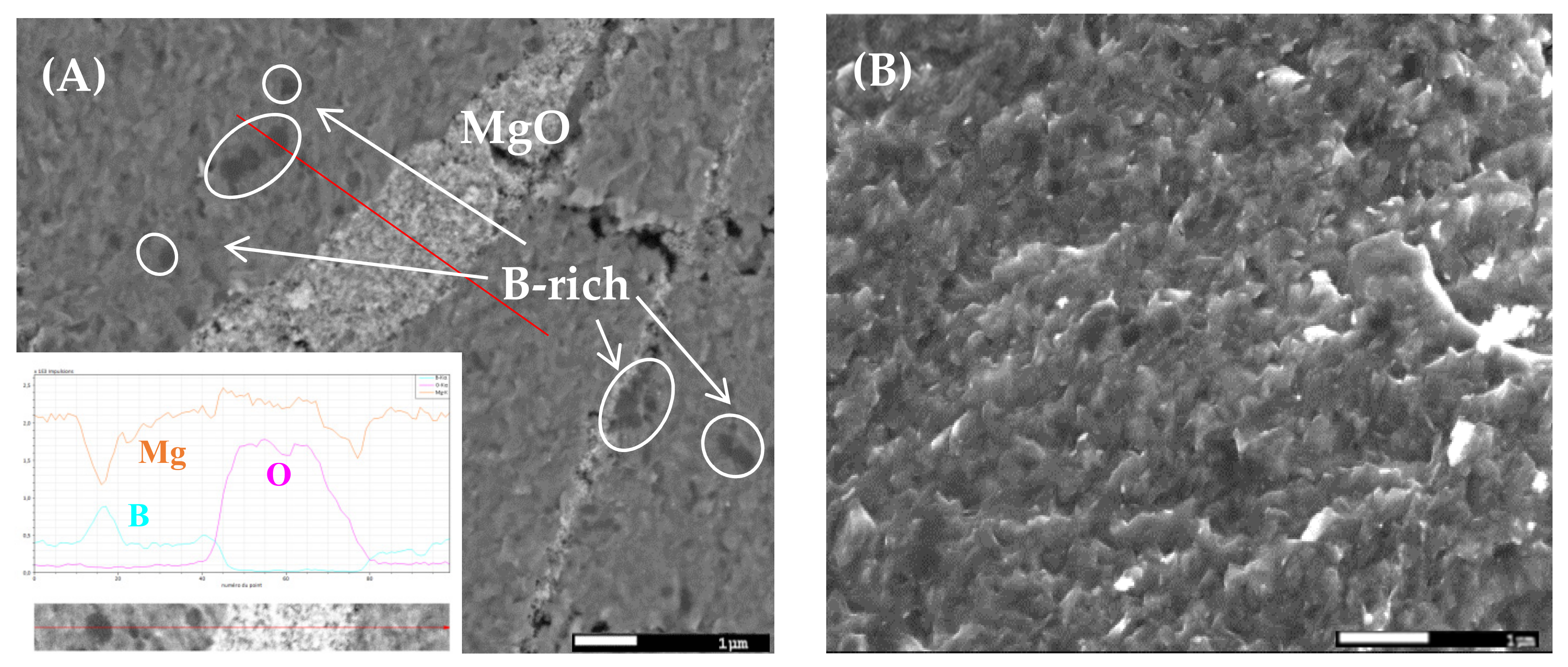
The microstructure of the fracture surface of sample A is shown in Figure 2. Its chemical compositions were examined using a back-scattered electron detector (see Figure 2A), and the topographic view of MgB2 grains was given by the secondary electron mode (see Figure 2B). Unreacted boron and MgO zones, which might have a flux-pinning-enhancing effect, are visible in Figure 2A. We underscore the presence of compact MgB2 nanograins and the high number of grain boundaries seen in Figure 2B.
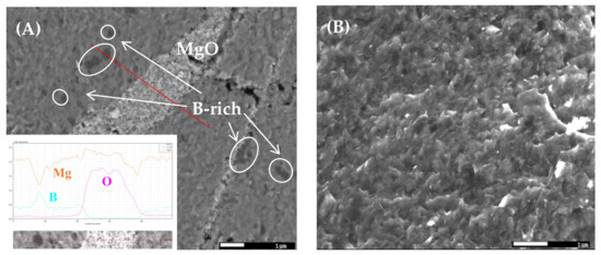
Figure 2.
(A) SEM micrograph of sample A showing the unreacted boron and MgO regions in the MgB2 matrix. (B) High-magnification SEM image of nano MgB2 grains. The inset of Figure 2A shows the EDS red-line region scan curves of boron (cyan line), oxygen (magenta line) and magnesium (orange line).
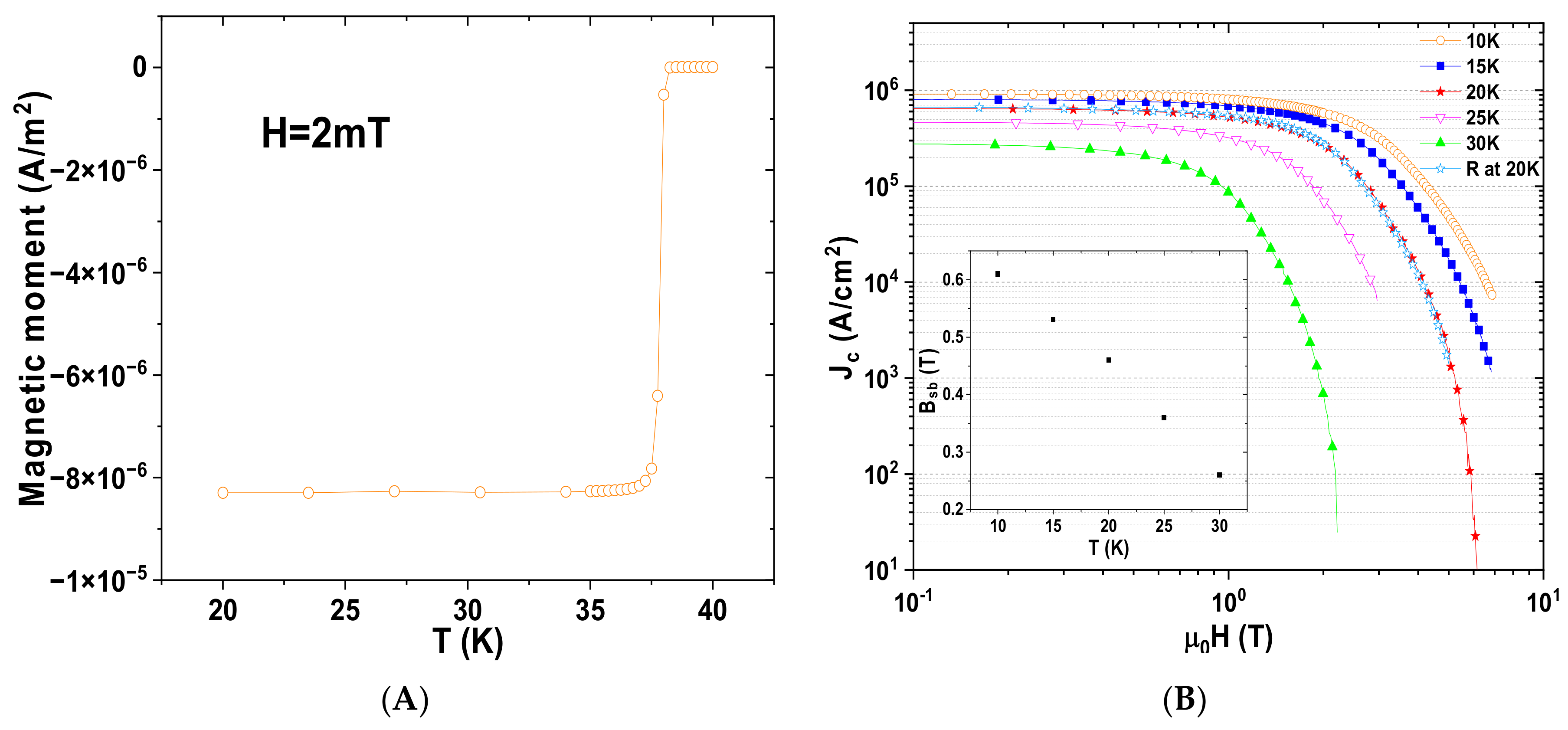
The magnetic moment of sample A as a function of the temperature is plotted in Figure 3A. The onset of the superconducting transition occurred at 38.25 K, and there was a narrow transition width (ΔT around 1 K). As shown in Figure 3B, for low values of field B, the critical current density Jc showed an invariant behavior with respect to the applied magnetic field; this plateau became smaller and smaller as the temperature increased. This behavior may indicate that the grain connectivity, or the packing ratio, which influences Jc in the self-field [23], is very good in the samples. This behavior is well-described by the ‘collective pinning’ model [24] with a dynamic state of the ‘single vortex’ flux pinning regime. This flux dynamic regime reveals the importance of defects in nanometric dimensions at the grain boundaries in this applied magnetic field range (Figure 2B). For larger values of the magnetic field, a crossover field, Bsb, from a ‘single vortex’ to a ‘small-flux bundle’, can be identified from the change in slope in Figure 3B. The inset in Figure 3B shows Bsb (T), which, as expected, is a decreasing function of the temperature. This quantity corresponds to the field for which Jc(B) = 0.95 ∗ Jc(0) [25]. This behavior due to the ‘boundle flux pinning’ regime for higher applied B values shows a critical current exponential decrease [23]. It is probable that in this magnetic region, the grains boundaries of the very small grains present in the material could dominate the pinning behavior in a high magnetic field [26]. At 20 K, a high Jc = 6.75 × 10⁵ A/cm2 in the self-field was measured. Remarkably, under 4 T, the critical current density was above 104 A/cm2, which is an extremely high critical current density at this temperature. Another possibility is that the pinning was due to the tensile stresses between the MgO precipitates or the areas rich in boron visible in Figure 2A on the one hand and the MgB2 zones on the other hand. This phenomenon was previously observed in a SiC-MgB2 bulk [4], where for B ≈ 4 T and T = 20 K, Jc was reported to be in the range of the values presented here.
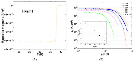
Figure 3.
(A) Magnetic moment of sample A as a function of the temperature. (B) Magnetic field dependence of the critical current density Jc of sample A at various temperatures. The figure also shows Jc for sample R at 20 K (blue stars). The inset shows the crossover field Bsb as a function of temperature.
Table 1 summarizes the best Jc of non-doped MgB2 bulks prepared by other authors, correlated with their density and grain size. As compared to these results, except for the samples prepared by high-pressure processing (HP) [27,28], a significant improvement in the critical current density in both the low and high field can be observed. This can be attributed to the strong densification of the nanograins, suggesting that it is possible to enhance the grain connectivity by increasing the pressure and decreasing the temperature applied during spark plasma sintering. In addition, the processing time is generally shorter than that required by the other techniques. The high Jc values recorded by Prikhna et al. (using HP processing) [27,28] are slightly higher than our results because their samples had a smaller grain size and higher density. However, the required sintering pressure and temperature were far greater than those required for the SPS process.

Table 1.
Characterization of MgB2 bulks prepared using different techniques.
The same critical current densities were measured for both samples, as can be seen in Figure 3B. In addition, at 10 K, Jc for sample A was equal to 9.1 × 10⁵ A/cm2 and 1.8 × 10⁴ A/cm2 at 0 and 6 T, respectively. From the application point of view, we underscore Jc values equal to 4.6 × 10⁵ A/cm2 and 2.7 × 10⁵ A/cm2 at 25 K and 30 K in the self-field, respectively. These high Jc values are compatible with the use of liquid hydrogen or neon as cooling fluids cheaper than liquid helium.
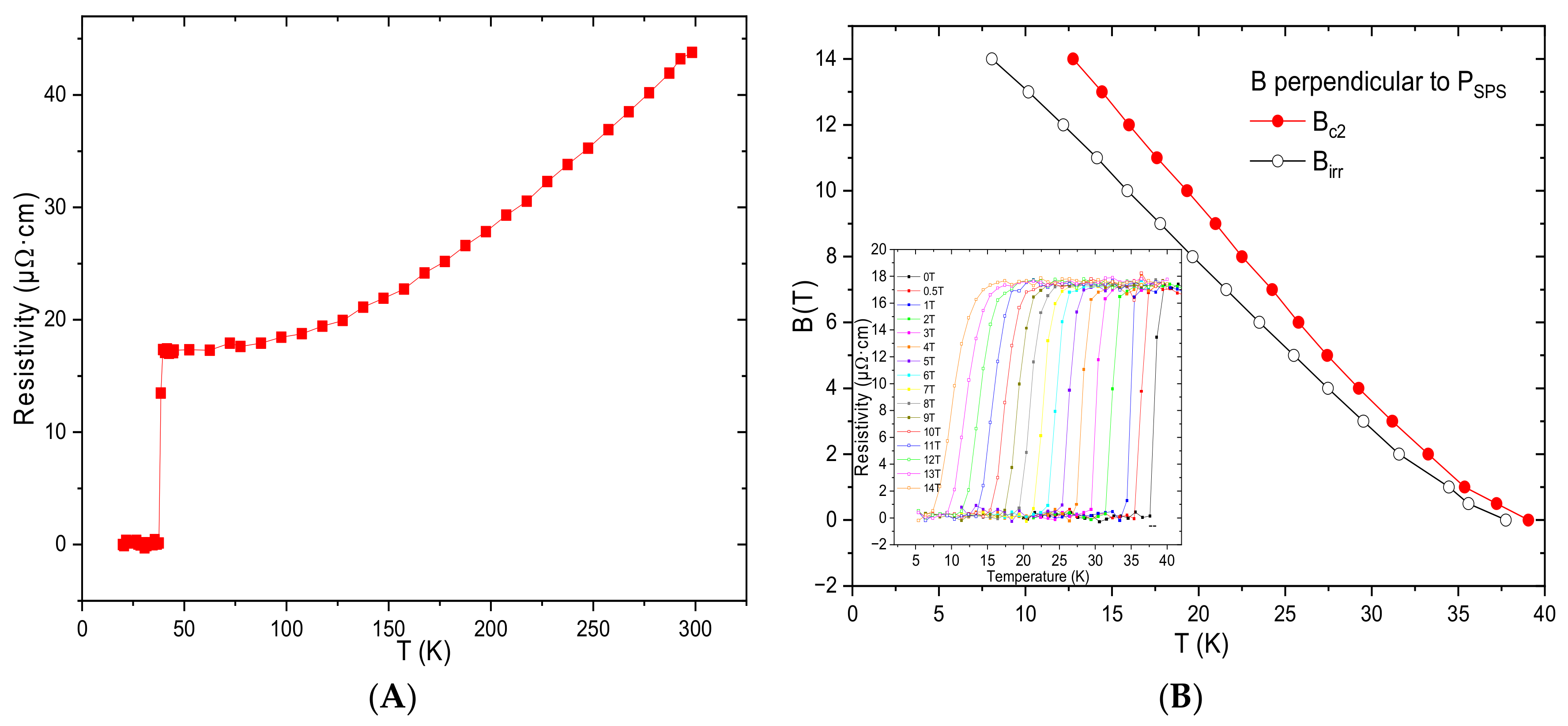
Concerning the electrical properties, the resistivity ρ as a function of the temperature is plotted in Figure 4A. It was equal to 43.8 µΩcm at 300 K and decreased to 17.1 µΩcm at 40 K. The residual resistivity ratio (RRR) was 2.56, which is close to the results obtained with other polycrystalline MgB2 bulks [23,34]. The upper critical magnetic field, Bc2, and the irreversibility magnetic field, Birr, were determined from 90% and 10% of ρ40K, as reported elsewhere [34,35]. From measurements of the resistivity carried out from 6 K to 40 K at fields ranging between 0 T and 14 T, their temperature dependence could be determined and is plotted in Figure 4B. The linear extrapolation of Bc2 and Birr at 0 K was 21.3 and 18.2 T, respectively. These values are higher than those reported for undoped MgB2 bulks [36].
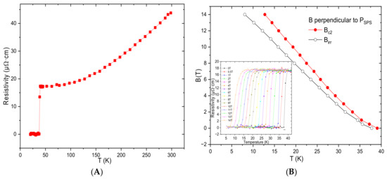
Figure 4.
(A) Temperature dependence of the resistivity of sample A at 0 T with a 5 mA direct current. (B) Temperature dependence of Bc2 and Birr for the same sample. The inset shows the resistivity transition at fields ranging between 0 T and 14 T with a direction perpendicular to the SPS sintering pressure.
4. Conclusions
We investigated the superconducting properties of a dense MgB2 sample processed by reactive sintering at 750 °C under 300 MPa using unconventional spark plasma sintering—SPS. The high packing factor of 95% enhanced the grain connectivity and sample density. A remarkable increase in critical current density values was observed. This indicates a strong vortex pinning effect attributed to the formation of nanograins and a large quantity of grain boundaries. The performances could probably be improved by optimizing the applied pressure, the sintering time and the precursor doping. This will be the objectives of our future studies.
Author Contributions
Conceptualization, Y.X., P.B., M.M. and J.G.N.; methodology, Y.X., P.B., M.M. and J.G.N.; software, Y.X.; validation, Y.X., P.B, M.M. and J.G.N.; formal analysis, Y.X., P.B., M.M. and J.G.N.; investigation, Y.X., P.B., M.M. and J.G.N.; resources, J.G.N. and M.M.; data curation, Y.X., P.B., M.M. and J.G.N.; writing—original draft preparation, Y.X., P.B., M.M. and J.G.N.; writing—review and editing, Y.X., P.B., M.M. and J.G.N.; visualization, Y.X., P.B., M.M. and J.G.N.; supervision, P.B., M.M. and J.G.N.; project administration, M.M. and J.G.N.; funding acquisition, M.M. All authors have read and agreed to the published version of the manuscript.
Funding
This work was partly supported by Shibaura Institute of Technology (SIT) International Research Center for Green Electronics and Grant-in-Aid FD research budget code: 721MA56383.
Institutional Review Board Statement
Not applicable.
Informed Consent Statement
Not applicable.
Data Availability Statement
Data available in a publicly accessible repository.
Acknowledgments
Y.X. thanks the “Conseil Régional-Normandie, France” for her thesis grant. The authors thank Jerôme Lecourt and Christelle Bilot for their technical support.
Conflicts of Interest
The authors declare no conflict of interest.
References
- Buzea, C.; Yamashita, T. Review of the Superconducting Properties of MgB2. Supercond. Sci. Technol. 2001, 14, R115. [Google Scholar] [CrossRef]
- Nagamatsu, J.; Nakagawa, N.; Muranaka, T.; Zenitani, Y.; Akimitsu, J. Akimitsu Superconductivity at 39 K in Magnesium Diboride. Nature 2001, 410, 63–64. [Google Scholar] [CrossRef] [PubMed]
- Muralidhar, M.; Kenta, N.; Koblischka, M.R.; Murakami, M. High Critical Current Densities in Bulk MgB2 Fabricated Using Amorphous Boron. Phys. Status Solidi (A) 2015, 212, 2141–2145. [Google Scholar] [CrossRef]
- Li, W.; Dou, S.-X. High Critical Current Density MgB2. In Superconductors-New Developments; IntechOpen: London, UK, 2015. [Google Scholar] [CrossRef]
- Yamamoto, A.; Ishihara, A.; Tomita, M.; Kishio, K. Permanent Magnet with MgB2 Bulk Superconductor. Appl. Phys. Lett. 2014, 105, 032601. [Google Scholar] [CrossRef]
- Baghdadi, R.; Arpaia, R.; Stepantsov, E.; Arzeo, M.; Golubev, D.; Montemurro, D.; Andersson, E.; Bauch, T.; Lombardi, F. Study of In-Plane Electrical Transport Anisotropy of a-Axis Oriented YBa2Cu3O7−δ Nanodevices. Phys. Rev. B 2017, 95, 184505. [Google Scholar] [CrossRef]
- Namburi, D.K.; Takahashi, K.; Hirano, T.; Kamada, T.; Fujishiro, H.; Shi, Y.-H.; Cardwell, D.A.; Durrell, J.H.; Ainslie, M.D. Pulsed-Field Magnetisation of Y-Ba-Cu-O Bulk Superconductors Fabricated by the Infiltration Growth Technique. Supercond. Sci. Technol. 2020, 33, 115012. [Google Scholar] [CrossRef]
- Kumakura, H.; Takano, Y.; Fujii, H.; Togano, K.; Kito, H.; Ihara, H. Critical Current Densities and Irreversibility Fields of MgB2 Bulks. Phys. C 2001, 363, 179–183. [Google Scholar] [CrossRef]
- Jung, S.-G.; Seong, W.K.; Kang, W.N. Effect of Columnar Grain Boundaries on Flux Pinning in MgB2 Films. J. Appl. Phys. 2012, 111, 053906. [Google Scholar] [CrossRef]
- Dezhin, D.; Ilyasov, R.; Dezhina, I. Development of Superconducting Propulsion System with Liquid Hydrogen Cooling for Future Electric Aircraft. In Proceedings of the 2020 International Conference on Electrotechnical Complexes and Systems (ICOECS), Ufa, Russia, 27–30 October 2020; pp. 1–3. [Google Scholar]
- Tokita, M. Development of Large-Size Ceramic/Metal Bulk FGM Fabricated by Spark Plasma Sintering. In Materials Science Forum; Trans Tech Publications Ltd.: Zürich, Switzerland, 1999; Volume 308, pp. 83–88. [Google Scholar] [CrossRef]
- Orrù, R.; Licheri, R.; Locci, A.M.; Cincotti, A.; Cao, G. Consolidation/Synthesis of Materials by Electric Current Activated/Assisted Sintering. Mater. Sci. Eng. R Rep. 2009, 63, 127–287. [Google Scholar] [CrossRef]
- Chaim, R.; Shen, Z. Grain Size Control by Pressure Application Regime during Spark Plasma Sintering of Nd-YAG Nanopowders. J. Mater. Sci. 2008, 43, 5023–5027. [Google Scholar] [CrossRef]
- Häßler, W.; Scheiter, J.; Hädrich, P.; Kauffmann-Weiß, S.; Holzapfel, B.; Oomen, M.; Nielsch, K. Properties of Ex-Situ MgB2 Bulk Samples Prepared by Uniaxial Hot Pressing and Spark Plasma SINTERING. Phys. C Supercond. Its Appl. 2018, 551, 48–54. [Google Scholar] [CrossRef]
- Shimada, Y.; Hata, S.; Ikeda, K.; Nakashima, H.; Matsumura, S.; Tanaka, H.; Yamamoto, A.; Shimoyama, J.; Kishio, K. Microstructural Connectivity in Sintered Ex-Situ MgB2 Bulk Superconductors. J. Alloys Compd. 2016, 656, 172–180. [Google Scholar] [CrossRef]
- Noudem, J.G.; Xing, Y.; Bernstein, P.; Retoux, R.; Higuchi, M.; Arvapalli, S.S.; Muralidhar, M.; Murakami, M. Improvement of Critical Current Density of MgB2 Bulk Superconductor Processed by Spark Plasma Sintering. J. Am. Ceram. Soc. 2020, 103, 6169–6175. [Google Scholar] [CrossRef]
- Noudem, J.; Dupont, L.; Bernstein, P.; Retoux, R.; Chevallier, G.; Estournès, C.; Berger, K.; Higuchi, M.; Muralidhar, M.; Murakami, M. Chapter 8—Superconducting Cryo-Magnets Processed by Spark Plasma Sintering and Texturing. In Spark Plasma Sintering; Cao, G., Estournès, C., Garay, J., Orrù, R., Eds.; Elsevier: Amsterdam, The Netherlands, 2019; pp. 185–199. ISBN 978-0-12-817744-0. [Google Scholar]
- de Terris, T.; Andreau, O.; Peyre, P.; Adamski, F.; Koutiri, I.; Gorny, C.; Dupuy, C. Optimization and Comparison of Porosity Rate Measurement Methods of Selective Laser Melted Metallic Parts. Addit. Manuf. 2019, 28, 802–813. [Google Scholar] [CrossRef]
- Sauerzopf, F.M.; Wiesinger, H.P.; Weber, H.W. Anisotropic Current Flow and Demagnetization Corrections in the Bean Model. Cryogenics 1990, 30, 650–655. [Google Scholar] [CrossRef]
- Lutterotti, L.; Matthies, S.; Wenk, H. MAUD (material analysis using diffraction): A user friendly Java program for Rietveld texture analysis and more. In Proceedings of the Twelfth International Conference on Textures of Materials (ICOTOM-12), Montreal, QC, Canada, 9–13 August 1999; NRC Research Press: Ottawa, ON, Canada, 1999; Volume 1. [Google Scholar]
- Kim, J.H.; Dou, S.X.; Shi, D.Q.; Rindfleisch, M.; Tomsic, M. Study of MgO Formation and Structural Defects in In Situ Processed MgB2 /Fe Wires. Supercond. Sci. Technol. 2007, 20, 1026–1031. [Google Scholar] [CrossRef]
- Sahu, P. Lattice Imperfections in Intermetallic Ti–Al Alloys: An X-Ray Diffraction Study of the Microstructure by the Rietveld Method. Intermetallics 2006, 14, 180–188. [Google Scholar] [CrossRef]
- Yamamoto, A.; Shimoyama, J.; Kishio, K.; Matsushita, T. Limiting Factors of Normal-State Conductivity in Superconducting MgB2: An Application of Mean-Field Theory for a Site Percolation Problem. Supercond. Sci. Technol. 2007, 20, 658–666. [Google Scholar] [CrossRef]
- Blatter, G.; Feigel’man, M.V.; Geshkenbein, V.B.; Larkin, A.I.; Vinokur, V.M. Vortices in High-Temperature Superconductors. Rev. Mod. Phys. 1994, 66, 1125–1388. [Google Scholar] [CrossRef]
- Xu, X.; Dou, S.X.; Wang, X.L.; Kim, J.H.; Stride, J.A.; Choucair, M.; Yeoh, W.K.; Zheng, R.K.; Ringer, S.P. Graphene Doping to Enhance the Flux Pinning and Supercurrent Carrying Ability of a Magnesium Diboride Superconductor. Supercond. Sci. Technol. 2010, 23, 085003. [Google Scholar] [CrossRef]
- Matsushita, T. MgB2. In Flux Pinning in Superconductors; Matsushita, T., Ed.; Springer Series in Solid-State Sciences; Springer: Berlin/Heidelberg, Germany, 2014; pp. 377–403. ISBN 978-3-642-45312-0. [Google Scholar]
- Prikhna, T.; Eisterer, M.; Gawalek, W.; Kozyrev, A.; Weber, H.W.; Sokolovsky, V.; Chaud, X.; Noudem, J.; Habisreuther, T.; Moshchil, V.; et al. Synthesis Pressure–Temperature Effect on Pinning in MgB2-Based Superconductors. J. Supercond. Nov. Magn. 2013, 26, 1569–1576. [Google Scholar] [CrossRef]
- Prikhna, T.; Eisterer, M.; Gawalek, W.; Mamalis, A.G.; Kozyrev, A.; Kovylaev, V.; Hristoforou, E.; Weber, H.W.; Noudem, J.G.; Goldacker, W.; et al. Structure and Functional Properties of Bulk MgB2 Superconductors Synthesized and Sintered under Pressure. In Materials Science Forum; Trans Tech Publications Ltd.: Zürich, Switzerland, 2014; Volume 792, pp. 21–26. [Google Scholar] [CrossRef]
- Mustapić, M.; Horvat, J.; Hossain, M.S.; Skoko, Ž.; Dou, S. Enhancing Superconducting Properties of MgB2 Pellets by Addition of Amorphous Magnetic Ni–Co–B Nanoparticles. Supercond. Sci. Technol. 2013, 26, 075013. [Google Scholar] [CrossRef]
- Muralidhar, M.; Nozaki, K.; Kobayashi, H.; Zeng, X.L.; Koblischka-Veneva, A.; Koblischka, M.R.; Inoue, K.; Murakami, M. Optimization of Sintering Conditions in Bulk MgB2 Material for Improvement of Critical Current Density. J. Alloys Compd. 2015, 649, 833–842. [Google Scholar] [CrossRef]
- Bhagurkar, A.G.; Yamamoto, A.; Babu, N.H.; Durrell, J.H.; Dennis, A.R.; Cardwell, D.A. Synthesis of Dense Bulk MgB2 by an Infiltration and Growth Process. Supercond. Sci. Technol. 2015, 28, 015012. [Google Scholar] [CrossRef]
- Zou, J.; Ainslie, M.D.; Fujishiro, H.; Bhagurkar, A.G.; Naito, T.; Babu, N.H.; Fagnard, J.-F.; Vanderbemden, P.; Yamamoto, A. Numerical Modelling and Comparison of MgB2 Bulks Fabricated by HIP and Infiltration Growth. Supercond. Sci. Technol. 2015, 28, 075009. [Google Scholar] [CrossRef]
- Dadiel, J.L.; Naik, S.P.K.; Pęczkowski, P.; Sugiyama, J.; Ogino, H.; Sakai, N.; Kazuya, Y.; Warski, T.; Wojcik, A.; Oka, T.; et al. Synthesis of Dense MgB2 Superconductor via In Situ and Ex Situ Spark Plasma Sintering Method. Materials 2021, 14, 7395. [Google Scholar] [CrossRef] [PubMed]
- Xu, X.; Kim, J.H.; Hossain, M.S.A.; Park, J.S.; Zhao, Y.; Dou, S.X.; Yeoh, W.K.; Rindfleisch, M.; Tomsic, M. Phase Transformation and Superconducting Properties of MgB2 Using Ball-Milled Low Purity Boron. J. Appl. Phys. 2008, 103, 023912. [Google Scholar] [CrossRef]
- Kang, Won Nam Single-Crystal like MgB2 Thin Films Grown on c-Cut Sapphire Substrates. Prog. Supercond. Cryog. 2014, 16, 7–9. [CrossRef][Green Version]
- Shigeta, I.; Abiru, T.; Abe, K.; Nishida, A.; Matsumoto, Y. Temperature and Field Dependence of Magnetization of MgB2 Polycrystals. Phys. C Supercond. 2003, 392, 359–363. [Google Scholar] [CrossRef]
Publisher’s Note: MDPI stays neutral with regard to jurisdictional claims in published maps and institutional affiliations. |
© 2022 by the authors. Licensee MDPI, Basel, Switzerland. This article is an open access article distributed under the terms and conditions of the Creative Commons Attribution (CC BY) license (https://creativecommons.org/licenses/by/4.0/).

