Article

NaCl-Assisted Chemical Vapor Deposition of Large-Domain Bilayer MoS2 on Soda-Lime Glass

1
School of Electronic Information, University of Electronic Science and Technology of China, Zhongshan Institute, Zhongshan 528402, China
2
School of Information and Communication Engineering, University of Electronic Science and Technology of China, Chengdu 611731, China
*
Author to whom correspondence should be addressed.
Nanomaterials 2022, 12(17), 2913; https://doi.org/10.3390/nano12172913
Submission received: 6 August 2022 / Revised: 19 August 2022 / Accepted: 20 August 2022 / Published: 24 August 2022

Abstract

:
In recent years, two-dimensional molybdenum disulfide (MoS2) has attracted extensive attention in the application field of next-generation electronics. Compared with single-layer MoS2, bilayer MoS2 has higher carrier mobility and has more promising applications for future novel electronic devices. Nevertheless, the large-scale low-cost synthesis of high-quality bilayer MoS2 still has much room for exploration, requiring further research. In this study, bilayer MoS2 crystals grown on soda-lime glass substrate by sodium chloride (NaCl)-assisted chemical vapor deposition (CVD) were reported, the growth mechanism of NaCl in CVD of bilayer MoS2 was analyzed, and the effects of molybdenum trioxide (Mo) mass and growth pressure on the growth of bilayer MoS2 under the assistance of NaCl were further explored. Through characterization with an optical microscope, atomic force microscopy and Raman analyzer, the domain size of bilayer MoS2 prepared by NaCl-assisted CVD was shown to reach 214 μm, which is a 4.2X improvement of the domain size of bilayer MoS2 prepared without NaCl-assisted CVD. Moreover, the bilayer structure accounted for about 85%, which is a 2.1X improvement of bilayer MoS2 prepared without NaCl-assisted CVD. This study provides a meaningful method for the growth of high-quality bilayer MoS2, and promotes the large-scale and low-cost applications of CVD MoS2.

1. Introduction

In recent years, with the rapid development of microelectronic devices, microelectronic technology based on silicon materials has encountered some bottlenecks, such as high power consumption, size reduction and slow performance improvement. New technology and material research is the key factor that is expected to break through the current technological bottlenecks [1,2,3]. Therefore, two-dimensional transition metal dichalcogenides (TMDs) have attracted extensive research attention due to their unique electronic and optoelectronic properties [4,5,6]. Among these two-dimensional TMDs, molybdenum disulfide (MoS2) has received the most extensive research attention [7,8,9,10,11]. Compared with graphene, MoS2 has greater advantages in transistor application because of its band gap, high switching ratio and strong inhibition of the short-channel effect [12,13]. Compared with silicon transistors, MoS2 transistors present lower power consumption and better inhibition of the short-channel effect [9,14]. For instance, based on side-wall MoS2 transistors, the physical channel length of transistors can reach 0.34 nm [9].
To realize the industry-compatible integration of these applications, the batch production of high-quality and large-crystal MoS2 films at low cost is of great importance. In the early stages of MoS2 research, diverse preparation methods were reported [15]. Xia et al. synthesized MoS2 crystals through a hydrothermal reaction followed by low-temperature crystallization annealing [16]. Eda et al. obtained large-scale few-layer MoS2 by ultrasound-assisted lithium intercalation exfoliation [17]. However, the layer number and size of MoS2 prepared by the above methods are difficult to control. Lou et al. used vapor-phase vulcanization to deposit a nano-scale Mo source on SiO2 sheets for sulphuration, and obtained continuous few-layer MoS2 films [18]. However, this method is very likely to cause a decrease in crystallinity, thereby leading to reduced mobility [19]. In the research on MoS2, chemical vapor deposition (CVD) is generally used over other methods. Wang et al. successfully prepared MoS2 crystals by CVD using sulfur (S) powder and molybdenum trioxide (MoO3) as precursors and SiO2/Si as a growth substrate [20], with the size reaching micrometers [21,22,23,24]. So far, the domain size of monolayer MoS2 crystal growth based on CVD has reached the millimeter level [25,26].
As we all know, in the CVD synthesis of MoS2, substrates play a critical role [27]. Moreover, in recent years, various substrates have been used in the growth of CVD MoS2 by different research groups [28,29,30,31]. Yang et al. synthesized highly oriented centimeter-scale MoS2 single crystals using gold foil as the growth substrate [31]. Li et al. prepared wafer-scale MoS2 single crystals on sapphire substrates through step-induced nucleation [10,32]. However, the triangular domain size of these MoS2 crystals is only tens of microns, and the cost of the sapphire and gold foil substrates is relatively high. In recent years, soda-lime glass has also received extensive attention in the research on growing MoS2 through CVD due to its advantages such as low cost, high growth rate, and large domain size [33,34,35,36]. As the growth substrate for MoS2, soda-lime glass has high fluidity under a high-temperature melting state, and can weaken lattice mismatch during the adsorption–diffusion–nucleation of precursor [4,27]. Additionally, Na+ released during melting can reduce the reaction barrier of MoS2 and promote its growth [37]. Chen et al. successfully grew high-quality millimeter-sized single-layer MoS2 on the molten soda-lime glass substrate through atmospheric pressure CVD [38], demonstrating the great advantages of the soda-lime glass substrate.
Compared with single-layer MoS2, bilayer MoS2 has a higher density of states and electron mobility due to its smaller indirect band gap, and retains the characteristics of atomic layer thickness [39], contributing to its higher potential in the field of novel electronic devices [11,13,40]. However, the large-scale growth of high-quality bilayer MoS2 on low-cost glass substrates still needs further research. For example, the domain size of CVD bilayer MoS2 single crystals is still about 200 μm [13,41], which is significantly smaller than the crystal size of monolayer MoS2. Recently, some research teams have tried to use some substances with a catalytic effect to assist the growth of MoS2, and achieved improved results [42,43,44,45]. Through the use of NaCl and Mo foil used as Mo source, Yang et al. successfully grew 100 μm high-quality bilayer MoS2 domains on soda-lime glass substrates by face-to-face CVD [46]. Nevertheless, this work focused on the synthesis of large-scale continuous MoS2 films, and the domain size of the bilayer MoS2 could be further improved by the optimization of growth conditions. Moreover, it has been shown that the growth rate of MoS2 from Mo in a 0-valence state is not as efficient as that of Mo in a 6-valence state in MoO3 [47]. However, nowadays, there is a lack of relevant research on directly introducing NaCl into MoO3 to assist high-quality bilayer MoS2 growth on low-cost soda-lime glass substrates.
In this work, we reported the results of CVD-based growth of bilayer MoS2 on melt soda-lime glass by introducing NaCl into the Mo source (MoO3). It was found that the introduction of NaCl could promote the growth of bilayer MoS2. Additionally, under NaCl-assisted growth, the synthesis of bilayer MoS2 crystals with different Mo masses and growth pressures was explored. Finally, by optimizing the process parameters, the size of bilayer MoS2 crystals was increased from the initial 50 μm to 214 μm, and the proportion of bilayer structure increased from the initial 40% to 85%. This study provides a valuable approach for the growth of bilayer MoS2 crystals, and is meaningful for the application of TMDs in future high-performance electronics.

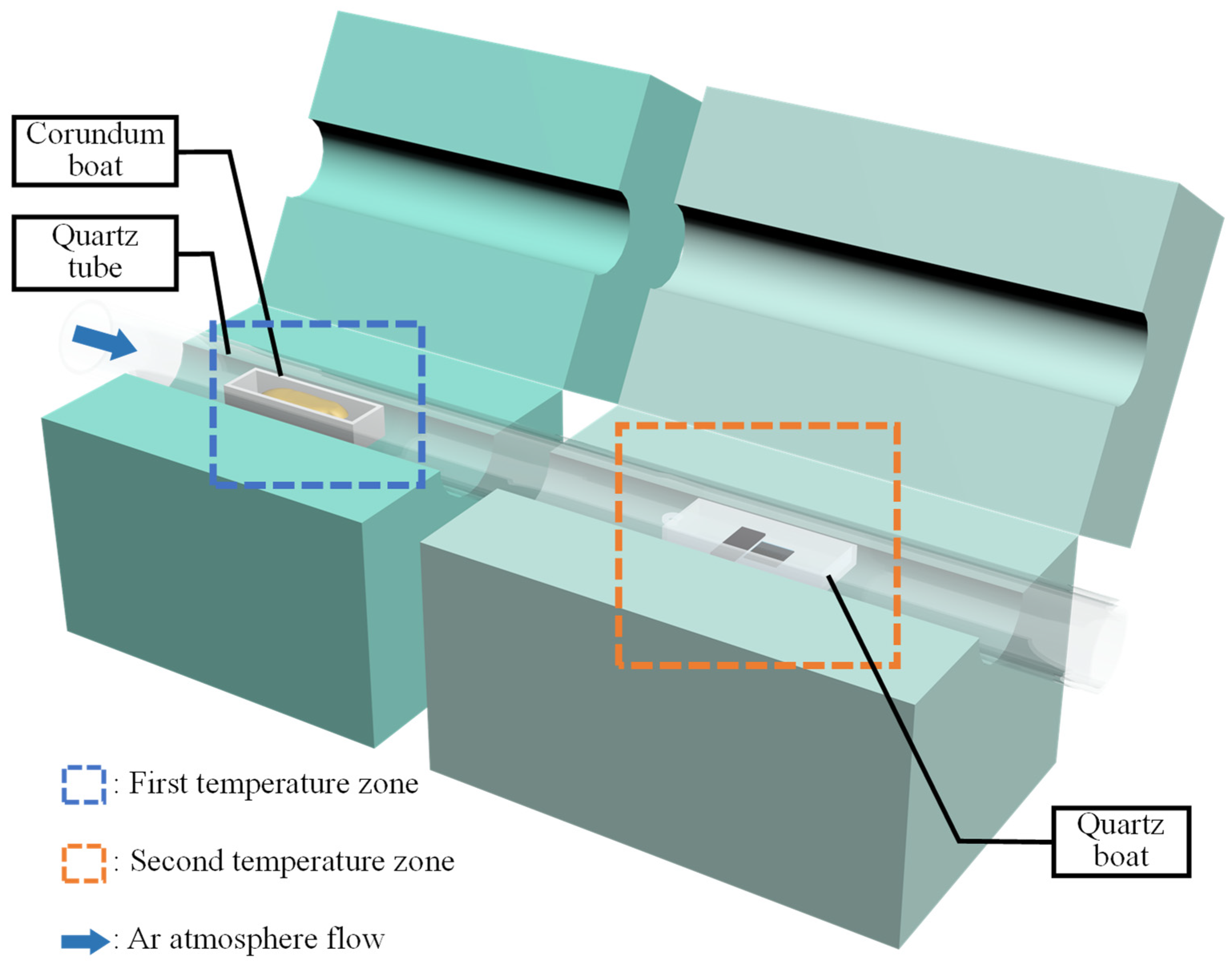
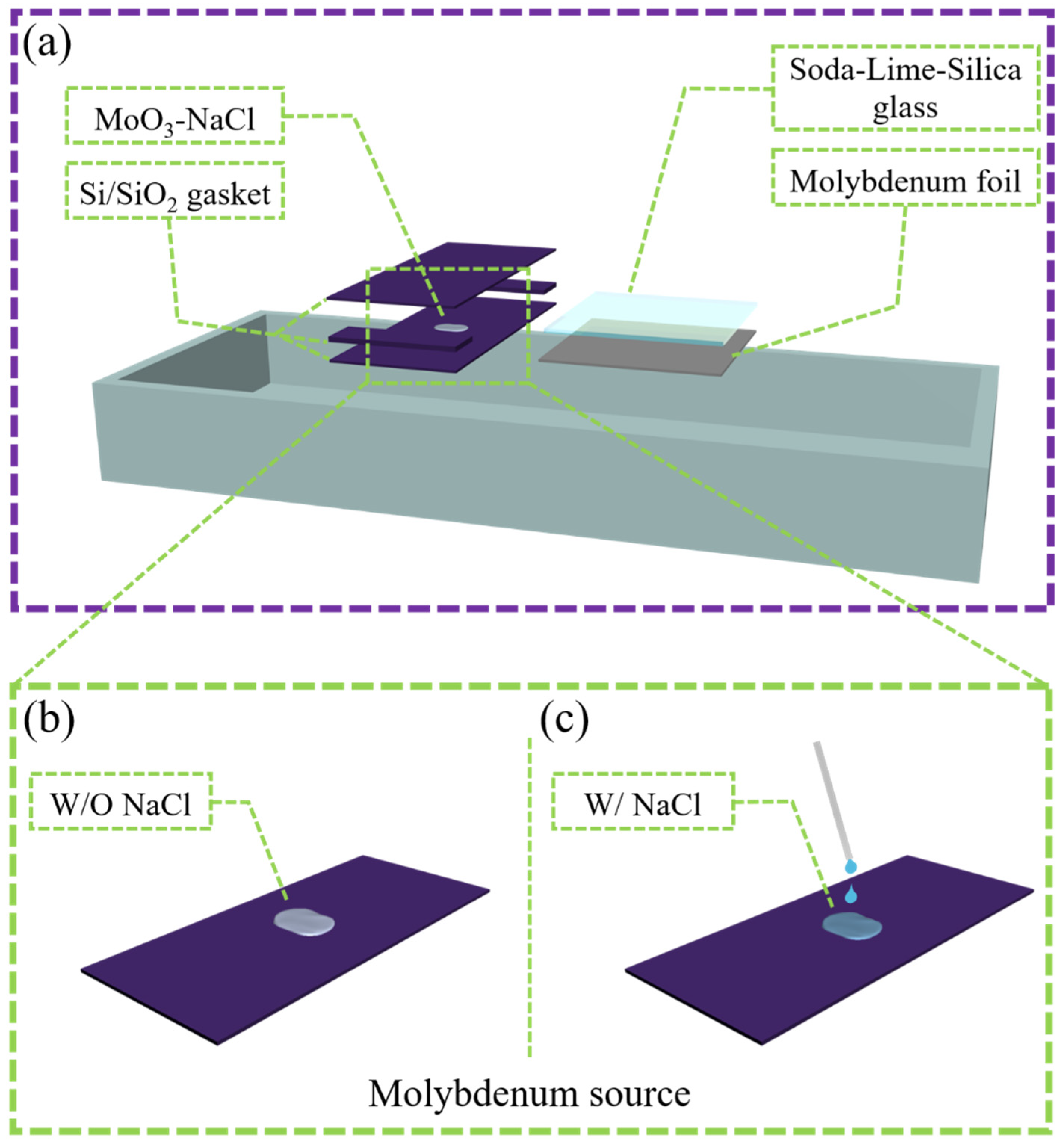
2. Experiments and Methods

In this study, bilayer MoS2 was prepared with the assistance of NaCl, with S powder and MoO3 powder as an S source and Mo source, respectively, and soda-lime glass as the growth substrate. The schematic setup of the experiment is shown in Figure 1. This system adopted a double-temperature-zone tubular furnace for heating. The S source was placed in the corundum boat in the first temperature zone. The Mo source-growth booster and substrate were loaded into the quartz boat in the second temperature zone. In addition, to prevent the soda-lime glass substrate from melting and sticking to the quartz boat at high temperatures, Mo foil was needed under the soda-lime glass. After mixing NaCl solution and MoO3 powder on the silicon wafer and drying, the mixture was placed in the quartz boat, and then the Mo foil gasket and soda-lime glass substrate were placed on the right side. The quartz boat and the corundum boat containing S powder were placed in the two temperature zones of the CVD furnace, respectively. The temperatures of the S and NaCl-MoO3 sources were 200 °C and 890 °C, respectively. High-purity argon was loaded, with a flow rate of 20 sccm. During the growth, the CVD system was kept at atmospheric pressure for 10 min. After growth, the morphology and size of bilayer MoS2 were characterized by optical microscope and Raman spectroscopy. The sample images were collected using optical microscopy combined with CCD (OM, BX51M, OLYMPUS, Tokyo, Japan ) and an atomic force microscopy (Dimension Edge, Bruker, Karlsruhe, Germany). Raman spectra were analyzed by an embedded Raman spectrometer (K-Swns-523, ideaoptics, Shanghai, China).
In this work, NaCl solution was directly mixed with MoO3 and dried as a Mo source for CVD-based growth of bilayer MoS2. The placement methods of the Mo source and substrate are presented in Figure 2. The Mo source was loaded into the quartz boat with SiO2/Si, which was covered with SiO2/Si cover plate to form a microcavity to prevent direct contact with S and poisoning during CVD. The soda-lime glass substrate was placed 3 mm to the right of the Mo source (at the downstream of the atmosphere flow), and the Mo foil was placed below to prevent it from sticking to the quartz boat after melting at high temperature.

3. Results and Discussion

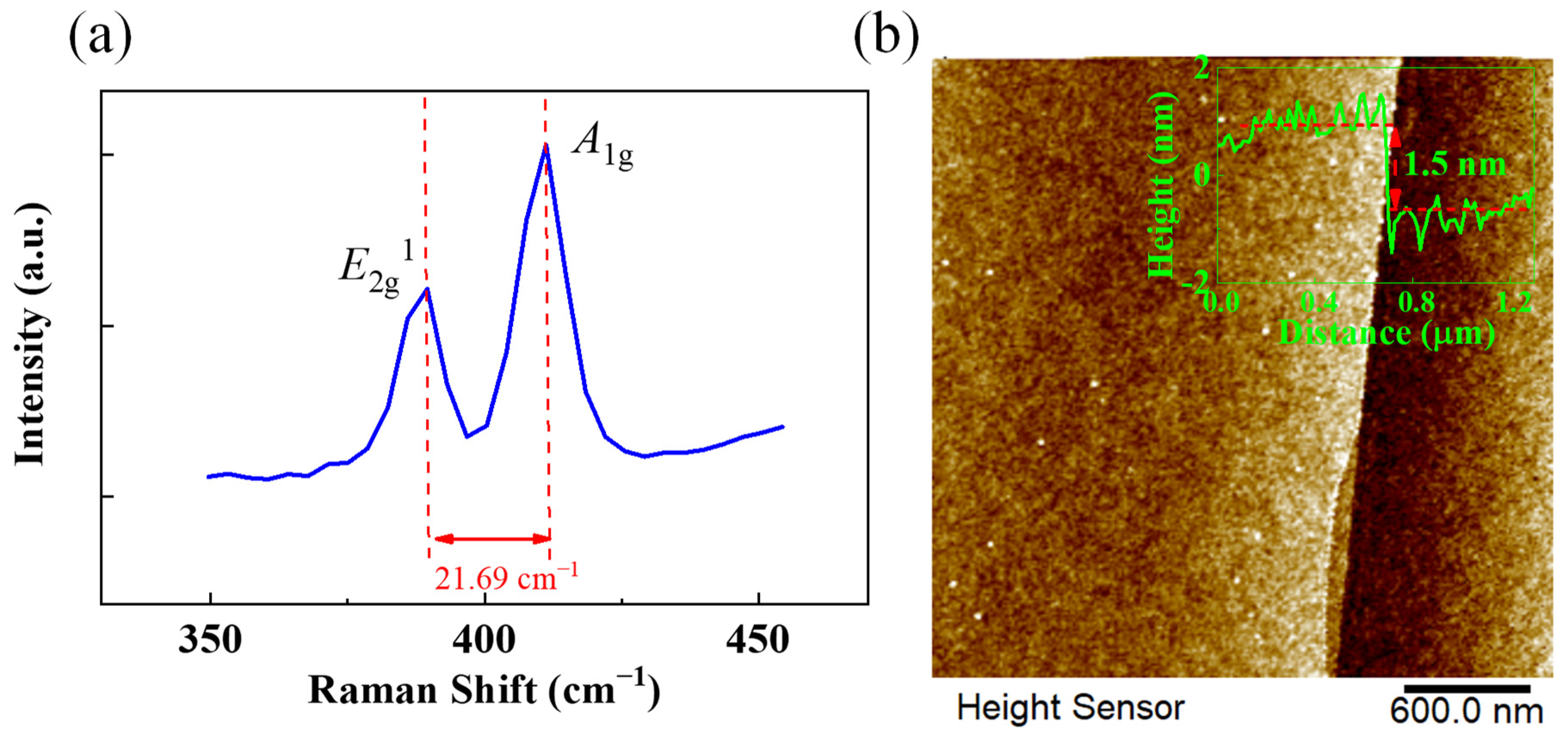
3.1. NaCl-Assisted Growth of Bilayer MoS2

To explore the effect of NaCl on the growth of bilayer MoS2, a series of comparative experiments were carried out. First, with other growth conditions unchanged, the effects of NaCl assistance and non-NaCl assistance on the growth of bilayer MoS2 on the glass substrate were investigated. During the experiment, the temperature and mass of the S source were 200 °C and 1.4 g, the temperature and mass of the Mo source were 890 °C and 4 mg, and the growth pressure was 1000 mbar. In the NaCl group, the proportion of NaCl solution/MoO3 was 1 mL/300 mg, and the concentration of NaCl was 5 mol/L. After adding NaCl, drying was performed at 50 °C for 5 min for subsequent growth operations. The growth results were obtained through the use of an optical microscope and are shown in Figure 3. Through comparison, it was found that among the bilayer MoS2 obtained in the NaCl group, the crystal size and the proportion of the bilayer structure to monolayer structure increased significantly. Without NaCl addition, the proportion of the bilayer structure in the grown MoS2 crystals was about 40%, and the bilayer size was about 50 μm. With NaCl added, the proportion of bilayer structure in the MoS2 crystals was about 85%, and the bilayer size was about 100 μm. The comparison of these experimental results showed that alkaline metal halides could significantly promote bilayer crystal growth during the preparation of transition metal halides. The increased bilayer MoS2 domain size and proportion of bilayer structure has could contribute to the following two aspects: Firstly, MoO3 reacts with NaCl at a high temperature to produce an intermediate product (molybdenum dichloride dioxide, Cl2MoO2; melting point—184 °C), which can be evaporated rapidly compared with the high melting point of MoO3, reducing the temperature of the gas-phase reaction, and providing more Mo sources during the same period [44,48]. Additionally, Na in NaCl and melted soda-lime glass can be used as the nucleation initiation factor of MoS2, which can reduce the reaction barrier [37].

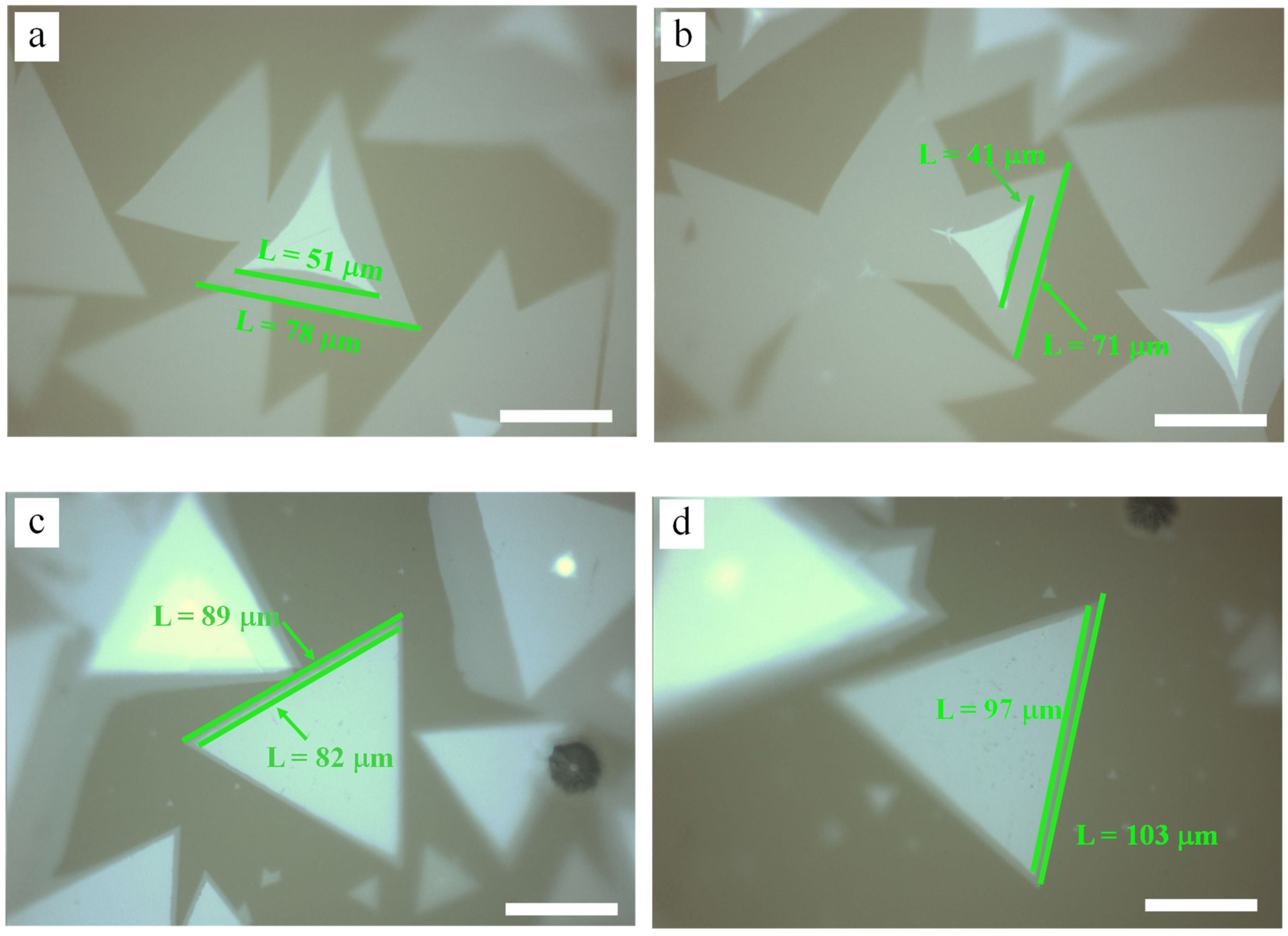
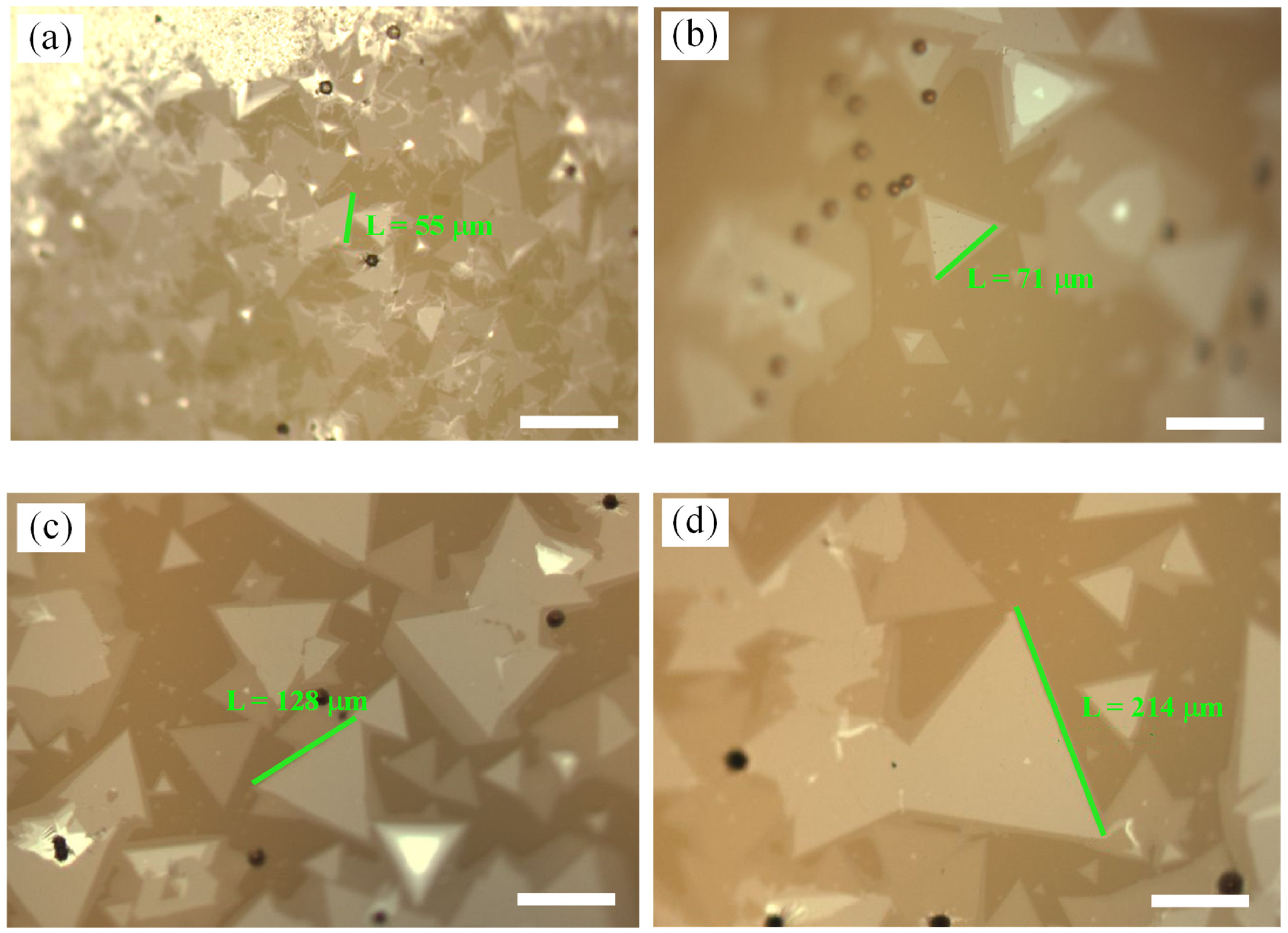
3.2. Effect of Mo Mass under NaCl Assistance

A large number of studies have shown that the mass of precursors has an important effect on the growth of MoS2 [4,6,13,37]. Under NaCl-assisted growth, we studied the effect of changing Mo mass on the growth of bilayer MoS2. With NaCl/MoO3 = 1 mL/300 mg (NaCl concentration was 5 mol/L) and other process parameters unchanged (i.e., the temperature and mass of S source were 200 °C and 1.4 g; the temperature of Mo source was 890 °C; the growth pressure was 1000 mbar; and the growth time was 8 min), the effects of Mo sources with different masses (3 mg, 3.5 mg, 4 mg, and 4.5 mg) on the growth of bilayer MoS2 on the glass substrate were explored. The growth results were obtained through the use of an optical microscope and are shown in Figure 4. The morphologies of bilayer MoS2 in Figure 4a–d are consistent, presenting an equilateral triangle, with a high proportion of bilayer structure. Meanwhile, with the increase in Mo mass, the size of bilayer MoS2 domains also increased obviously, with the maximum size reaching 120 μm. This phenomenon is consistent with our previous work without NaCl assistance [13]. With the CVD process located in the mass transport limited region, higher precursor mass flux can contribute to a higher diffusion rate through boundary layer, resulting in overcoming the mass transport limit and promoting single domain growth [49,50].

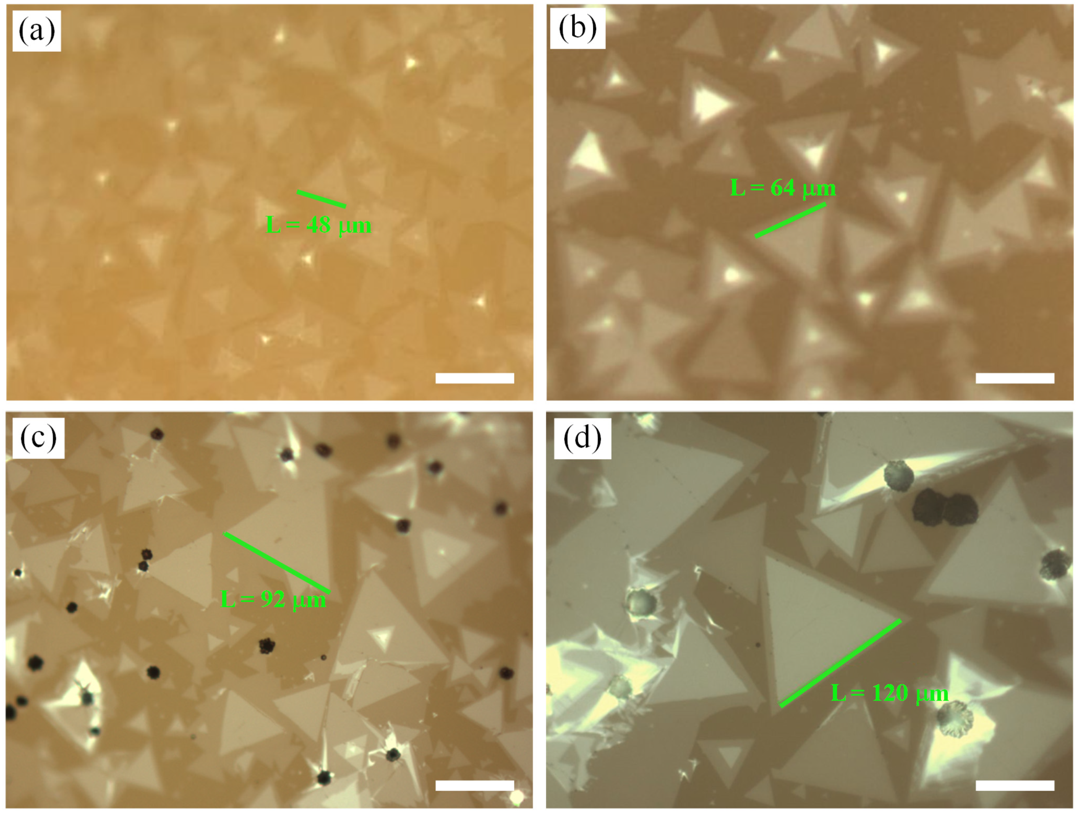
3.3. Effect of Growth Pressure under NaCl Assistance

In addition, with the assistance of NaCl, we further explored the effect of reaction pressure on the growth of bilayer MoS2 on the glass substrate. Similarly, with the mass ratio of NaCl/MoO3 and other growth conditions unchanged, different growth pressures (1100 mbar, 1000 mbar, 900 mbar, and 700 mbar) were used, and the growth results were obtained through the use of an optical microscope and are shown in Figure 5a–d. The size of bilayer MoS2 domains increased gradually with the gradual decrease in pressure, and the size of bilayer MoS2 single crystal growth at 700 mbar reached 214 μm, which is comparable to the largest bilayer MoS2 domain reported in literature [13,41]. The large bilayer MoS2 domain could be attributable to the assistance of NaCl and the low growth pressure. With the assistance of NaCl, the molybdenum oxychloride precursor with a low melting point produced volatilizes rapidly at high temperature, breaking the self-limiting growth of monolayer MoS2 [44], and then causing secondary nucleation and the synchronous growth of the bilayer structure. Moreover, under low pressure, the precursor diffused faster on the melted substrate, which contributed to the growth rate of bilayer structures closer to that of single-layer structures [37]. Therefore, the size of bilayer MoS2 could be greatly increased while maintaining a high proportion of the bilayer structure.
Raman characterization is an important means to characterize the growth results of MoS2, which can reflect the layer number and quality of MoS2. In this study, the bilayer MoS2 crystals prepared under different pressures were characterized and analyzed by Raman spectroscopy. The Raman spectral characterization results are shown in Figure 6a. The characteristic peak E2g1 and A1g of bilayer MoS2 crystals in the Raman spectral were located at 389.54 cm−1 and 411.23 cm−1, respectively, and the difference between the characteristic peaks was 21.69 cm−1. This result is consistent with the Raman characteristic peak position and difference of bilayer MoS2 in other studies, indicating that high-quality bilayer MoS2 crystals are obtained [51,52]. Furthermore, to demonstrate the bilayer nature of the MoS2 domains, Figure 6b displays the atomic force microscopy (AFM) images obtained from an edge of bilayer MoS2 domain. A thickness of 1.5 nm was demonstrated through the AFM characterization, which is consistent with the thickness of bilayer MoS2 in other works [13,53].

4. Conclusions

In summary, this study systematically investigates the NaCl-assisted growth of bilayer MoS2 on the soda-lime glass substrate. The results show that the introduction of NaCl plays a very important role in the growth of bilayer MoS2, and improves the proportion of bilayer structure and the size of bilayer MoS2 crystals. In addition, the effects of two important growth parameters, Mo mass and growth pressure, on the growth of bilayer MoS2 on the glass substrate under the assistance of NaCl are explored. The results reveal that, under certain conditions, the size of bilayer MoS2 crystals increases with the increase in Mo mass. Moreover, by changing growth pressure, the size of bilayer MoS2 crystals is significantly increased, and the domain size of bilayer MoS2 crystals is larger than 200 μm, with the bilayer structure accounting for about 85%. This study provides an interesting method worthy of further research for the growth of high-quality bilayer MoS2 and has significance for promoting the further large-scale low-cost synthesis and industrial application of two-dimensional MoS2.

Author Contributions

Conceptualization, Q.G. and L.C.; methodology, Q.G., L.C., S.C., C.Z. and X.P.; validation, Q.G. and Z.Z.; formal analysis, Q.G., P.L., Z.Y., L.C. and F.C.; investigation, Q.G, L.C.; resources, Q.G., C.Z., L.L., J.Y. and L.L.; data curation, Q.G.; writing—original draft preparation, Q.G. and L.C.; writing—review and editing, Q.G. and L.C.; visualization, L.C.; supervision, Q.G. and S.C.; project administration, Q.G. and C.Z.; funding acquisition, Q.G. and C.Z. All authors have read and agreed to the published version of the manuscript.

Funding

This work was funded in part by the Natural Science Foundation of China (Grant Nos. 62104033, 62071088 and 11775047), in part by the Guangdong Basic and Applied Basic Research Foundation (Grant No. 2019A1515110752), in part by the Youth Innovative Talent Project of Guangdong Education Department (Grant No. 2019KQNCX187), in part by the Outstanding Chinese and Foreign Youth Exchange Program of China Association for Science and Technology (CAST) 2019, in part by the Project for Innovation Team of Guangdong University (Grant Nos. 2018KCXTD033, 2020KCXTD030 and 2021KCXTD040), in part by the Construction Project of Professional Quality Engineering in 2022 (Grant No. YLZY202201), in part by the key scientific research project of the Department of Education of Guangdong Province (Grant No. 2021ZDZX1052), and in part by National Key R&D Program of China (Grant No. 2018YFB1801302).

Data Availability Statement

The data that support the findings of this study are available from the corresponding author upon reasonable request.

Conflicts of Interest

The authors declare no conflict of interest.

References

  1. Akinwande, D.; Petrone, N.; Hone, J. Two-dimensional flexible nanoelectronics. Nat. Commun. 2014, 5, 5678. [Google Scholar] [CrossRef] [PubMed]
  2. Sangwan, V.K.; Hersam, M.C. Electronic transport in two-dimensional materials. Annu. Rev. Phys. Chem. 2018, 69, 299–325. [Google Scholar] [CrossRef] [PubMed] [Green Version]
  3. Akinwande, D.; Huyghebaert, C.; Wang, C.-H.; Serna, M.I.; Goossens, S.; Li, L.-J.; Wong, H.S.P.; Koppens, F.H.L. Graphene and two-dimensional materials for silicon technology. Nature 2019, 573, 507–518. [Google Scholar] [CrossRef]
  4. Seravalli, L.; Bosi, M. A review on chemical vapour deposition of two-dimensional MoS2 flakes. Materials 2021, 14, 7590. [Google Scholar] [CrossRef]
  5. Zhang, X.; Grajal, J.; Vazquez-Roy, J.L.; Radhakrishna, U.; Wang, X.; Chern, W.; Zhou, L.; Lin, Y.; Shen, P.-C.; Ji, X.; et al. Two-dimensional MoS2-enabled flexible rectenna for Wi-Fi-band wireless energy harvesting. Nature 2019, 566, 368–372. [Google Scholar] [CrossRef] [PubMed]
  6. Tang, L.; Tan, J.; Nong, H.; Liu, B.; Cheng, H.-M. Chemical vapor deposition growth of two-dimensional compound materials: Controllability, material quality, and growth mechanism. Acc. Mater. Res. 2021, 2, 36–47. [Google Scholar] [CrossRef]
  7. Mutalik, C.; Krisnawati, D.I.; Patil, S.B.; Khafid, M.; Atmojo, D.S.; Santoso, P.; Lu, S.-C.; Wang, D.-Y.; Kuo, T.-R. Phase-dependent MoS2 nanoflowers for light-driven antibacterial application. ACS Sustain. Chem. Eng. 2021, 9, 7904–7912. [Google Scholar] [CrossRef]
  8. Gao, Q.; Lu, J.; Chen, S.; Chen, L.; Xu, Z.; Lin, D.; Xu, S.; Liu, P.; Zhang, X.; Cai, W.; et al. Chemical vapor deposition of uniform and large-domain molybdenum disulfide crystals on glass/Al2O3 substrates. Nanomaterials 2022, 12, 2719. [Google Scholar] [CrossRef]
  9. Wu, F.; Tian, H.; Shen, Y.; Hou, Z.; Ren, J.; Gou, G.; Sun, Y.; Yang, Y.; Ren, T.-L. Vertical MoS2 transistors with sub-1-nm gate lengths. Nature 2022, 603, 259–264. [Google Scholar] [CrossRef]
  10. Liu, L.; Li, T.; Ma, L.; Li, W.; Gao, S.; Sun, W.; Dong, R.; Zou, X.; Fan, D.; Shao, L.; et al. Uniform nucleation and epitaxy of bilayer molybdenum disulfide on sapphire. Nature 2022, 605, 69–75. [Google Scholar] [CrossRef]
  11. Gao, Q.; Zhang, C.; Yi, Z.; Pan, X.; Chi, F.; Liu, L.; Li, X.; Wu, Y. Improved low-frequency noise in CVD bilayer MoS2 field-effect transistors. Appl. Phys. Lett. 2021, 118, 153103. [Google Scholar] [CrossRef]
  12. Li, X.; Yang, L.; Si, M.; Li, S.; Huang, M.; Ye, P.; Wu, Y. Performance potential and limit of MoS2 transistors. Adv. Mater. 2015, 27, 1547–1552. [Google Scholar] [CrossRef] [PubMed]
  13. Gao, Q.; Zhang, Z.; Xu, X.; Song, J.; Li, X.; Wu, Y. Scalable high performance radio frequency electronics based on large domain bilayer MoS2. Nat. Commun. 2018, 9, 4778. [Google Scholar] [CrossRef] [PubMed]
  14. Desai, S.B.; Madhvapathy, S.R.; Sachid, A.B.; Llinas, J.P.; Wang, Q.; Ahn, G.H.; Pitner, G.; Kim, M.J.; Bokor, J.; Hu, C.; et al. MoS2 transistors with 1-nanometer gate lengths. Science 2016, 354, 99. [Google Scholar] [CrossRef] [PubMed] [Green Version]
  15. Xu, H.; Zhu, J.; Ma, Q.; Ma, J.; Bai, H.; Chen, L.; Mu, S. Two-dimensional MoS2: Structural properties, synthesis methods, and regulation strategies toward oxygen reduction. Micromachines 2021, 12, 240. [Google Scholar] [CrossRef]
  16. Xia, B.; An, L.; Gao, D.; Shi, S.; Xi, P.; Xue, D. Hierarchical ultrathin Mo(SxSe1−x)2 nanosheets with tunable ferromagnetism and efficient hydrogen evolution reaction activity: Towards defect site effect. CrystEngComm 2015, 17, 6420–6425. [Google Scholar] [CrossRef]
  17. Eda, G.; Yamaguchi, H.; Voiry, D.; Fujita, T.; Chen, M.; Chhowalla, M. Correction to photoluminescence from chemically exfoliated MoS2. Nano Lett. 2012, 12, 526. [Google Scholar] [CrossRef]
  18. Zhan, Y.; Liu, Z.; Najmaei, S.; Ajayan, P.M.; Lou, J. Large-area vapor-phase growth and characterization of MoS2 atomic layers on a SiO2 substrate. Small 2012, 8, 966–971. [Google Scholar] [CrossRef] [Green Version]
  19. Shi, Y.; Li, H.; Li, L.-J. Recent advances in controlled synthesis of two-dimensional transition metal dichalcogenides via vapour deposition techniques. Chem. Soc. Rev. 2015, 44, 2744–2756. [Google Scholar] [CrossRef]
  20. Wang, X.; Feng, H.; Wu, Y.; Jiao, L. Controlled synthesis of highly crystalline MoS2 flakes by chemical vapor deposition. J. Am. Chem. Soc. 2013, 135, 5304–5307. [Google Scholar] [CrossRef]
  21. Amani, M.; Chin, M.L.; Birdwell, A.G.; O’Regan, T.P.; Najmaei, S.; Liu, Z.; Ajayan, P.M.; Lou, J.; Dubey, M. Electrical performance of monolayer MoS2 field-effect transistors prepared by chemical vapor deposition. Appl. Phys. Lett. 2013, 102, 193107. [Google Scholar] [CrossRef] [Green Version]
  22. Liu, H.; Si, M.; Najmaei, S.; Neal, A.T.; Du, Y.; Ajayan, P.M.; Lou, J.; Ye, P.D. Statistical study of deep submicron dual-gated field-effect transistors on monolayer chemical vapor deposition molybdenum disulfide films. Nano Lett. 2013, 13, 2640–2646. [Google Scholar] [CrossRef] [PubMed] [Green Version]
  23. van der Zande, A.M.; Huang, P.Y.; Chenet, D.A.; Berkelbach, T.C.; You, Y.; Lee, G.-H.; Heinz, T.F.; Reichman, D.R.; Muller, D.A.; Hone, J.C. Grains and grain boundaries in highly crystalline monolayer molybdenum disulphide. Nat. Mater. 2013, 12, 554–561. [Google Scholar] [CrossRef] [PubMed] [Green Version]
  24. Kim, I.S.; Sangwan, V.K.; Jariwala, D.; Wood, J.D.; Park, S.; Chen, K.-S.; Shi, F.; Ruiz-Zepeda, F.; Ponce, A.; Jose-Yacaman, M.; et al. Influence of stoichiometry on the optical and electrical properties of chemical vapor deposition derived MoS2. ACS Nano 2014, 8, 10551–10558. [Google Scholar] [CrossRef] [Green Version]
  25. Ji, Q.; Su, C.; Mao, N.; Tian, X.; Idrobo, J.-C.; Miao, J.; Tisdale William, A.; Zettl, A.; Li, J.; Kong, J. Revealing the Brønsted-Evans-Polanyi relation in halide-activated fast MoS2 growth toward millimeter-sized 2D crystals. Sci. Adv. 2021, 7, eabj3274. [Google Scholar] [CrossRef]
  26. Zhang, Z.; Zhu, L.; Wang, D.; Tang, B.; Yang, P.; Shi, Y.; Zhou, F.; Fu, J.; Huan, Y.; Cui, F.; et al. Ultrafast growth of large-area uniform, millimeter-size MoSe2 single crystals on low-cost soda-lime glass. Adv. Mater. Interfaces 2021, 8, 2100415. [Google Scholar] [CrossRef]
  27. Qin, B.; Ma, H.; Hossain, M.; Zhong, M.; Xia, Q.; Li, B.; Duan, X. Substrates in the synthesis of two-dimensional materials via chemical vapor deposition. Chem. Mater. 2020, 32, 10321–10347. [Google Scholar] [CrossRef]
  28. Wang, Q.; Li, N.; Tang, J.; Zhu, J.; Zhang, Q.; Jia, Q.; Lu, Y.; Wei, Z.; Yu, H.; Zhao, Y.; et al. Wafer-scale highly oriented monolayer MoS2 with large domain sizes. Nano Lett. 2020, 20, 7193–7199. [Google Scholar] [CrossRef]
  29. Li, T.; Guo, W.; Ma, L.; Li, W.; Yu, Z.; Han, Z.; Gao, S.; Liu, L.; Fan, D.; Wang, Z.; et al. Epitaxial growth of wafer-scale molybdenum disulfide semiconductor single crystals on sapphire. Nat. Nanotechnol. 2021, 16, 1201–1207. [Google Scholar] [CrossRef]
  30. Zhang, Z.; Xu, X.; Song, J.; Gao, Q.; Li, S.; Hu, Q.; Li, X.; Wu, Y. High-performance transistors based on monolayer CVD MoS2 grown on molten glass. Appl. Phys. Lett. 2018, 113, 202103. [Google Scholar] [CrossRef]
  31. Yang, P.; Zhang, S.; Pan, S.; Tang, B.; Liang, Y.; Zhao, X.; Zhang, Z.; Shi, J.; Huan, Y.; Shi, Y.; et al. Epitaxial growth of centimeter-scale single-crystal MoS2 monolayer on Au(111). ACS Nano 2020, 14, 5036–5045. [Google Scholar] [CrossRef] [PubMed]
  32. Wu, D.; Shi, J.; Zheng, X.; Liu, J.; Dou, W.; Gao, Y.; Yuan, X.; Ouyang, F.; Huang, H. CVD grown MoS2 nanoribbons on MoS2 covered sapphire(0001) without catalysts. Phys. Status Solidi-Rapid Res. Lett. 2019, 13, 1900063. [Google Scholar] [CrossRef]
  33. Chen, Y.; Sun, J.; Gao, J.; Du, F.; Han, Q.; Nie, Y.; Chen, Z.; Bachmatiuk, A.; Priydarshi, M.K.; Ma, D.; et al. Growing uniform graphene disks and films on molten glass for heating devices and cell culture. Adv. Mater. 2015, 27, 7839–7846. [Google Scholar] [CrossRef] [PubMed]
  34. Liu, J.; Fu, L. Controllable growth of graphene on liquid surfaces. Adv. Mater. 2019, 31, 1800690. [Google Scholar] [CrossRef]
  35. Zeng, M.; Liu, J.; Zhou, L.; Mendes, R.G.; Dong, Y.; Zhang, M.-Y.; Cui, Z.-H.; Cai, Z.; Zhang, Z.; Zhu, D.; et al. Bandgap tuning of two-dimensional materials by sphere diameter engineering. Nat. Mater. 2020, 19, 528–533. [Google Scholar] [CrossRef]
  36. Cai, Q.; Ju, Q.; Hong, W.; Jian, C.; Wang, T.; Liu, W. Water assisted growth of two-dimensional MoS2/MoSe2 vertical heterostructures on molten glass. Nanoscale 2022, 14, 1990–1996. [Google Scholar] [CrossRef]
  37. Yang, P.; Zou, X.; Zhang, Z.; Hong, M.; Shi, J.; Chen, S.; Shu, J.; Zhao, L.; Jiang, S.; Zhou, X.; et al. Batch production of 6-inch uniform monolayer molybdenum disulfide catalyzed by sodium in glass. Nat. Commun. 2018, 9, 979. [Google Scholar] [CrossRef]
  38. Chen, J.; Zhao, X.; Tan, S.J.R.; Xu, H.; Wu, B.; Liu, B.; Fu, D.; Fu, W.; Geng, D.; Liu, Y.; et al. Chemical vapor deposition of large-size monolayer MoSe2 crystals on molten glass. J. Am. Chem. Soc. 2017, 139, 1073–1076. [Google Scholar] [CrossRef]
  39. Wang, H.; Yu, L.; Lee, Y.-H.; Shi, Y.; Hsu, A.; Chin, M.L.; Li, L.-J.; Dubey, M.; Kong, J.; Palacios, T. Integrated circuits based on bilayer MoS2 transistors. Nano Lett. 2012, 12, 4674–4680. [Google Scholar] [CrossRef] [Green Version]
  40. Gao, Q.; Zhang, C.; Yang, K.; Pan, X.; Zhang, Z.; Yang, J.; Yi, Z.; Chi, F.; Liu, L. High-performance CVD bilayer MoS2 radio frequency transistors and gigahertz mixers for flexible nanoelectronics. Micromachines 2021, 12, 451. [Google Scholar] [CrossRef]
  41. Wang, S.; Zhang, Y.; Zhao, D.; Li, J.; Kang, H.; Zhao, S.; Jin, T.; Zhang, J.; Xue, Z.; Wang, Y.; et al. Fast and controllable synthesis of AB-stacked bilayer MoS2 for photoelectric detection. 2D Mater. 2021, 9, 15016. [Google Scholar] [CrossRef]
  42. Li, S.; Wang, S.; Tang, D.-M.; Zhao, W.; Xu, H.; Chu, L.; Bando, Y.; Golberg, D.; Eda, G. Halide-assisted atmospheric pressure growth of large WSe2 and WS2 monolayer crystals. Appl. Mater. Today 2015, 1, 60–66. [Google Scholar] [CrossRef] [Green Version]
  43. Li, S.; Lin, Y.-C.; Zhao, W.; Wu, J.; Wang, Z.; Hu, Z.; Shen, Y.; Tang, D.-M.; Wang, J.; Zhang, Q.; et al. Vapour–liquid–solid growth of monolayer MoS2 nanoribbons. Nat. Mater. 2018, 17, 535–542. [Google Scholar] [CrossRef] [PubMed] [Green Version]
  44. Zhou, J.; Lin, J.; Huang, X.; Zhou, Y.; Chen, Y.; Xia, J.; Wang, H.; Xie, Y.; Yu, H.; Lei, J.; et al. A library of atomically thin metal chalcogenides. Nature 2018, 556, 355–359. [Google Scholar] [CrossRef]
  45. Chen, L.; Zang, L.; Chen, L.; Wu, J.; Jiang, C.; Song, J. Study on the catalyst effect of NaCl on MoS2 growth in a chemical vapor deposition process. CrystEngComm 2021, 23, 5337–5344. [Google Scholar] [CrossRef]
  46. Yang, P.; Zhang, Z.; Sun, M.; Lin, F.; Cheng, T.; Shi, J.; Xie, C.; Shi, Y.; Jiang, S.; Huan, Y.; et al. Thickness tunable wedding-cake-like MoS2 flakes for high-performance optoelectronics. ACS Nano 2019, 13, 3649–3658. [Google Scholar] [CrossRef] [Green Version]
  47. Salazar, N.; Beinik, I.; Lauritsen, J.V. Single-layer MoS2 formation by sulfidation of molybdenum oxides in different oxidation states on Au(111). Phys. Chem. Chem. Phys. 2017, 19, 14020–14029. [Google Scholar] [CrossRef]
  48. Kojima, K.; Lim, H.E.; Liu, Z.; Zhang, W.; Saito, T.; Nakanishi, Y.; Endo, T.; Kobayashi, Y.; Watanabe, K.; Taniguchi, T.; et al. Restoring the intrinsic optical properties of CVD-grown MoS2 monolayers and their heterostructures. Nanoscale 2019, 11, 12798–12803. [Google Scholar] [CrossRef] [Green Version]
  49. Bhaviripudi, S.; Jia, X.; Dresselhaus, M.S.; Kong, J. Role of kinetic factors in chemical vapor deposition synthesis of uniform large area graphene using copper catalyst. Nano Lett. 2010, 10, 4128–4133. [Google Scholar] [CrossRef]
  50. Zhou, S.; Gan, L.; Wang, D.; Li, H.; Zhai, T. Space-confined vapor deposition synthesis of two dimensional materials. Nano Res. 2018, 11, 2909–2931. [Google Scholar] [CrossRef]
  51. Verble, J.L.; Wieting, T.J. Lattice Mode Degeneracy in MoS2 and Other Layer Compounds. Phys. Rev. Lett. 1970, 25, 362–365. [Google Scholar] [CrossRef]
  52. Lee, C.; Yan, H.; Brus, L.E.; Heinz, T.F.; Hone, J.; Ryu, S. Anomalous lattice vibrations of single- and few-layer MoS2. ACS Nano 2010, 4, 2695–2700. [Google Scholar] [CrossRef] [PubMed] [Green Version]
  53. Zheng, J.; Yan, X.; Lu, Z.; Qiu, H.; Xu, G.; Zhou, X.; Wang, P.; Pan, X.; Liu, K.; Jiao, L. High-mobility multilayered MoS2 flakes with low contact resistance grown by chemical vapor deposition. Adv. Mater. 2017, 29, 1604540. [Google Scholar] [CrossRef] [PubMed]
Figure 1. Schematic setup of chemical vapor deposition (CVD) system.
Nanomaterials 12 02913 g001
Figure 2. Schematic of Mo source and substrate placement: (a) Schematic map of Mo source and substrate placement; (b,c) schematic of Mo source with or without NaCl addition.
Nanomaterials 12 02913 g002
Figure 3. Comparison of growth results of NaCl-assisted bilayer MoS2. (a,b) Growth results without NaCl. (c,d) Growth results with NaCl. (ad) The scale bars are 40 μm.
Nanomaterials 12 02913 g003
Figure 4. Growth results under different Mo sources masses assisted by NaCl: (a) 3 mg, (b) 3.5 mg, (c) 4 mg, and (d) 4.5 mg. (ad) The scale bars are 60 μm.
Nanomaterials 12 02913 g004
Figure 5. Growth results under different growth pressures assisted by NaCl. (a) The growth pressure is 1100 mbar. (b) The growth pressure is 1100 mbar. (c) The growth pressure is 900 mbar. (d) The growth pressure is 700 mbar. All scale bars are 100 μm.
Nanomaterials 12 02913 g005
Figure 6. (a) Raman spectral of bilayer MoS2; (b) AFM image of bilayer MoS2.
Nanomaterials 12 02913 g006
Publisher’s Note: MDPI stays neutral with regard to jurisdictional claims in published maps and institutional affiliations.

