Abstract
We propose a numerical compact model for describing the drain current in ballistic mode by using an expression to represent the transmission coefficients for all operating regions. This model is based on our previous study of an analytic compact model for the subthreshold region in which the DIBL and source-to-drain tunneling effects were both taken into account. This paper introduces an approach to establishing the smoothing function for expressing the critical parameters in the model’s overall operating regions. The resulting compact model was tested in a TCAD NEGF simulation, demonstrating good consistency.
1. Introduction
As electronic device dimensions shrink, nanoscale devices with multigate structures are considered to improve immunity to short-channel effects (SCEs), such as drain-induced barrier lowering (DIBL) and threshold voltage roll-off [1,2,3,4,5,6,7,8,9]. In recent years, several novel structures of devices [10,11,12,13,14,15,16,17], such as nanowire (NW) and nanosheet (NSH) metal-oxide semiconductor field-effect transistors (MOSFETs), have attracted more attention and become potential structures that most likely led to downscaling into the sub-7 nm regime. Then, because of the reduction in scattering events in the short-channel nanowire GAA MOSFETs, carriers traveling through the channel without scattering increase ballistic transport [18,19,20,21,22]. Thus, the properties of such devices in which the quantum transport of carriers should be taken into account were intensively investigated and modeled [23,24,25,26,27,28,29].
Moreover, since the DIBL effect cannot be neglected in an ultrashort channel gate-all-around (GAA) MOSFET, it is more meaningful to develop a compact model incorporating ballistic transport, quantum confinement, and quantum tunneling effects. Then, the ballistic transport and quantum mechanism in ultrashort channel nanowire GAA MOSFETs were widely recognized as significant factors in determining drain current characteristics by using a numerical calculation method such as Schrödinger–Poisson and nonequilibrium Green’s function (NEGF) simulations [30,31,32,33]. The results of the current characteristics from the TCAD simulation and the experiment both demonstrate higher and better subthreshold swing (SS) characteristics in a GAA MOSFET than those in a Fin field-effect transistor (FinFET) in a wide range of temperature. They also indicate that GAA MOSFETs can provide more robust solutions to next-CMOS devices beyond FinFETs and low-supply-voltage applications [29,34,35]. However, the computations of the simulations could be time-consuming, even for estimating the characteristics of one single device. A compact model of nanowire GAA MOSFETs would be more efficient in describing the drain-current characteristics for a reduction in computational time when taking the ballistic transport and quantum effects into account.
Several compact models evaluating GAA-MOSFET properties were reported [10,36,37,38,39,40,41,42,43,44,45,46]. Some models focused on the expressions of the drain-current characteristic with a DIBL effect, incorporating the transport modes on the basis of the drift-diffusion [39,44] and ballistic theories [41]. Although the DIBL effect is mentioned in some of those models, the quantum confinement [39,45] and the source-to-drain tunneling effects [10,41,42] also need to be considered in the models. Consequently, the drain current would be represented by combining tunneling and thermionic ballistic transport expressions in the subthreshold and inversion regions [47]. However, a fully analytic compact model that can be introduced to SPICE-class simulators using Verilog-A language to implement a circuit-level simulation is expected to be mathematically developed to predict the behavior of a nanowire GAA MOSFET as a final purpose. According to our previous work, the potential distribution of a sub-band energy level and transmission coefficient of the source-to-drain tunneling can be expressed and determined approximately by using one parabolic function and the Wentzel–Kramers–Brillouin (WKB) approximation, respectively. Although source-to-drain tunneling was incorporated in the ballistic device with an ultrashort channel according to our previous study [47], it is increasingly necessary to simplify the calculation process in a compact model when evaluating the drain current by only using the Landauer formula in all operating regions.
In this paper, we propose one numerical compact model of the nanowire GAA MOSFET with an ultrashort channel to describe the ballistic drain current by introducing an approach of the smoothing function to determine the significant parameters through connecting the expressions of the subthreshold and inversion regions mentioned in our previous study [24]. Hence, we improved expressing the unknown parameter, the barrier top locations, and the transmission coefficients for all operating regions using the smoothing functions mentioned above. Then, the drain current for the ultrashort channel GAA MOSFET is evaluated from the Landauer formula, which is in line with NEGF simulation results. The rest of this paper is organized as follows. We introduce the model structure, definition of parameters, and the ballistic current model in Section 2. Section 3 illustrates how we use the smoothing functions to approximately express the unknown parameter, the barrier top location, and the transmission coefficients being valid for all operating regions. Lastly, the calculation results and discussion are in Section 4.
2. Device Structure and Model Formulas
2.1. Model Structure
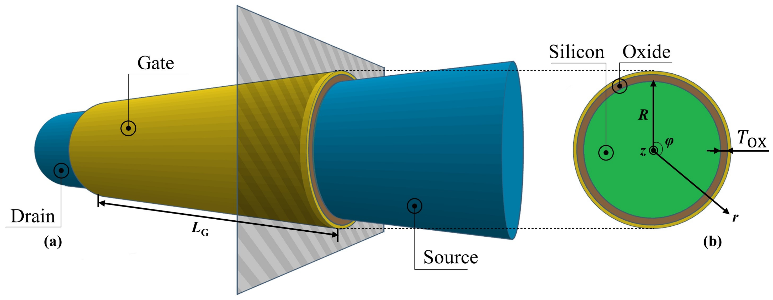
Figure 1a,b show the schematic structures of the modeled nanowire GAA MOSFETs in the channel and transverse directions, respectively. In this structural model, we consider the source and drain electrodes as the ideal reservoirs of electrons since they were produced with highly doped n-type silicon that would provide sufficient electrons into the intrinsic silicon channel surrounded by gate oxide and metal gate with a circular cross-section. Moreover, the backscattering from the source and drain electrodes was neglected. Channel length, radius, and gate oxide thickness are denoted as , R, and , respectively. Correspondingly, the cylindrical coordinate with length, radius, and angular components along with z, r, and directions, as shown in Figure 1b, is used in the following formulations. However, on account of the perfect angular symmetry in our model, it was sufficient to represent the electrostatic potential distribution only along the channel and radius directions without considering the component.
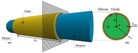
Figure 1.
Schematic structure (a) in the channel direction z and (b) in the transverse direction r of the nanowire GAA MOSFET model.
2.2. Potential Profile
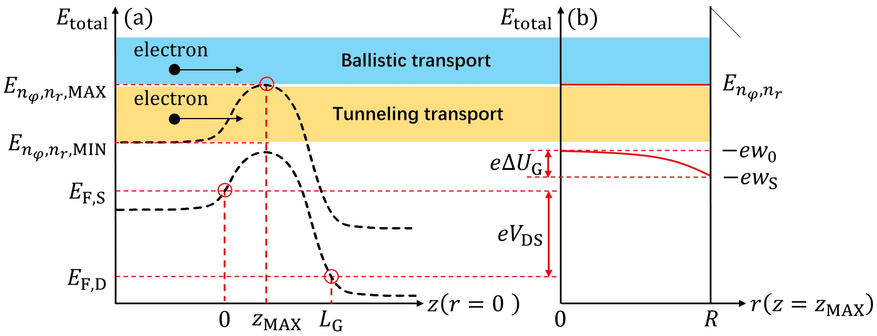
The profiles of the conduction band edge and the higher sub-band energy levels along the z and r axes at and are shown in Figure 2a,b, respectively, where it was assumed that the short-channel effects to the channel along the transverse direction in this model were consistent. Then, as shown in Figure 2a, is the total energy of an electron, and the maximal value of the sub-band energy within the channel was located at , where and are the angular and radial quantum numbers, respectively. The energy value around the source edge within the same sub-band is denoted as . Furthermore, and represent the Fermi energies at the source and drain, respectively, while the voltage across, expressing the difference of the electrostatic potential between the source and drain in Fermi level , is . The electrostatic potentials in the transverse direction at the center and surface of the cylindrical channel are defined as and , respectively, and the conduction band edges at the same locations are given by and , respectively, as illustrated in Figure 2b. Correspondingly, the difference between and was described using an unknown parameter, . Moreover, the higher sub-band energy levels measured from are . According to our previous study, can be written in terms of along the z axis as follows [6,22]:
where ℏ, , and are the Planck’s constant, the confinement electron effective mass in r axis, and the constant described as the -th zero point of the first-kind Bessel function with order , respectively, is the gate-source voltage, refers to the work function difference between the gate and the channel material, and is the conduction band edge at the flat-band condition corresponding to the relationship of . Moreover, is the perturbation matrix constant that was calculated in our previous work [24], denotes a geometric constant defined by , is the dielectric constant of the channel, and is the gate oxide capacitance per unit length. along the z axis is given by
where A and B are the coefficients related to the voltage between the gate/drain and the source, respectively; is the scaling coefficient depending on mentioned above that can be given by
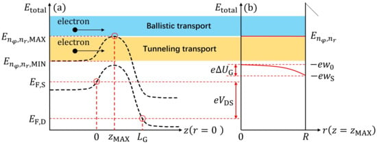
Figure 2.
Rough sketch of the potential energy profiles along the channel and the transverse directions, and mechanisms governing the carrier transport in ballistic tunneling and thermionic modes. (a) Representation of energy-level distribution along the z direction at the channel center (). (b) Schematics of confinement potential energy distribution along the r direction at the barrier top () in the cross-section. The elementary charge is denoted by e.
Accordingly, the above coefficients are given by:
where is the junction built-in potential between the source and channel that represents the electrostatic potential energy level of a sub-band at the source measured from [6]. In addition, the corresponding position to the barrier top of the sub-band energy level along the channel can be derived with:
2.3. Landauer Formula
Considering that the device channel length was shorter than 7 nm, electrons traveling through the device channel comprised the ones whose energies were higher or lower than the sub-band energy level at the barrier top. Thereby, the Landauer formula could determine the drain current contributed by the electrons in the ballistic transport between the source and drain with both the thermionic and tunneling modes. Then, the ballistic current between the drain and source in the channel can be written as follows [48]:
where is the valley index of the energy band, is the transmission coefficient of electrons tunneling through the source-to-drain barrier in the sub-band with quantum numbers of and at a given , which is the electron kinetic energy in the z direction, and refers to the Fermi–Dirac distribution. Here, denotes the transmission probability derived from the WKB approximation:
where is the electron effective mass along with the channel direction, and and are defined as the classical turning points at which is equal to the potential barrier energy.
3. Calculation Method
In this study, electrons carrying energy higher than the maximal potential barrier were transmitted from the source to the drain by thermionic emission. In comparison, electrons with lower energy can traverse the channel only by quantum tunneling through the potential barrier between the source and drain. However, it was assumed that electrons transporting from the drain could be neglected when calculating both the thermionic ballistic and the source-to-drain tunneling current calculations under the condition of high drain bias as , regardless of the electrons traveling over and through the potential energy barrier. Moreover, it was assumed that the ballistic current consists of electrons only excited to the lowest sub-band when and as the quantum numbers for all operating regions since no electrons are excited to the second or higher sub-band energy levels in the nanowire GAA MOSFET. Then, the carrier quantum reflection was considered to be negligible on the barrier in the channel. Nevertheless, in the channel of purely ballistic transport, the device behavior model could be simplified to describe the electrons’ transmission over and through the source-to-drain potential energy barrier in one consistent expression.
3.1. Parabolic Energy Level Approximation
Since WKB approximation was applied to calculate the transmission probability for the source-to-drain tunneling, it had to be evaluated by numerically integrating the classical turning points from Equation (12). Therefore, it could render the model analytically calculable by assuming that the sub-band energy profile along the device channel to be a parabolic function, which is valid in a short-channel device [47]. Then, when the channel length is sufficiently short, the lowest sub-band energy level along the z direction could be assumed to be approximately described by a parabolic function of z, denoted as [47]. This leads to the result below:
where and are given by Equation (1) at the positions when and , respectively, as follows:
Then, by substituting and into Equation (3), and can be derived in terms of A and B, related to the bias conditions:
3.2. Unknown Parameter for All Operating Regions
This study introduces and implements a mathematical approach for establishing the smoothing function by connecting two kinds of expressions in their different regions. In addition, this method requires two different expressions of an arbitrary function and a constant in the expressions’ respective ranges of values. Compared with the previous work on the unknown parameter at the top of the potential barrier in all operating regions [6], an alternative approach to represent was achieved. Implementing the smoothing function to represent in Equation (18), it was set as zero for a large gate voltage bias, while its expression was valid in the subthreshold region incorporating the DIBL effect. It could thus be rewritten as for all operating regions with the following formula:
where is a fitting constant to be adjusted for the best accuracy; this value was fixed to be for wide devices and bias conditions. To obtain a single valid expression for all operating regions, we blended with by following the same assumption as that in [24] as follows:
3.3. Potential Barrier Top for All Operating Regions
Furthermore, from analyzing Equation (8), the expression of was valid only in the subthreshold region and took meaningless values in the inversion region. According to the same inference in Section 3.2 to describe the smoothing function for a whole range of values, it could be assumed that , representing the distance between the locations of the source edge and the potential barrier top, decreased to nearly zero with the ever-increasing gate voltage. Thus, two expressions were needed to be given by Equation (8) and zero in the subthreshold and inversion regions, resectively. Then, the barrier top position in all operating regions was approximately evaluated as follows:
where is a fitting parameter without any physical meaning; this value was fixed to be for wide devices and bias conditions to achieve reasonable accuracy.
3.4. Transmission Coefficient for All Operating Regions
According to Equation (12), the tunneling transmission coefficient through a sub-band energy barrier could be expressed in two conditions corresponding to a given . Then, representing the sub-band energy level profile as a parabolic function, the tunneling transmission coefficient applying the WKB approximation to substitute Equation (13) into Equation (12) was determined as follows:
On the other hand, the transmission coefficient of the energy sub-band here was unity and corresponding to the electrons with the total energies of and , respectively. Here, varied between 0 and 1. Considering that the smoothing function requires the expressions given by and one in their ranges of values taking with and , the transmission coefficient for all operating regions could then be represented as follows:
where denotes the fitting parameter, and the value was set to be 1.5 to obtain a good agreement for all operating regions in the next section.
3.5. Drain Current for All Operating Regions
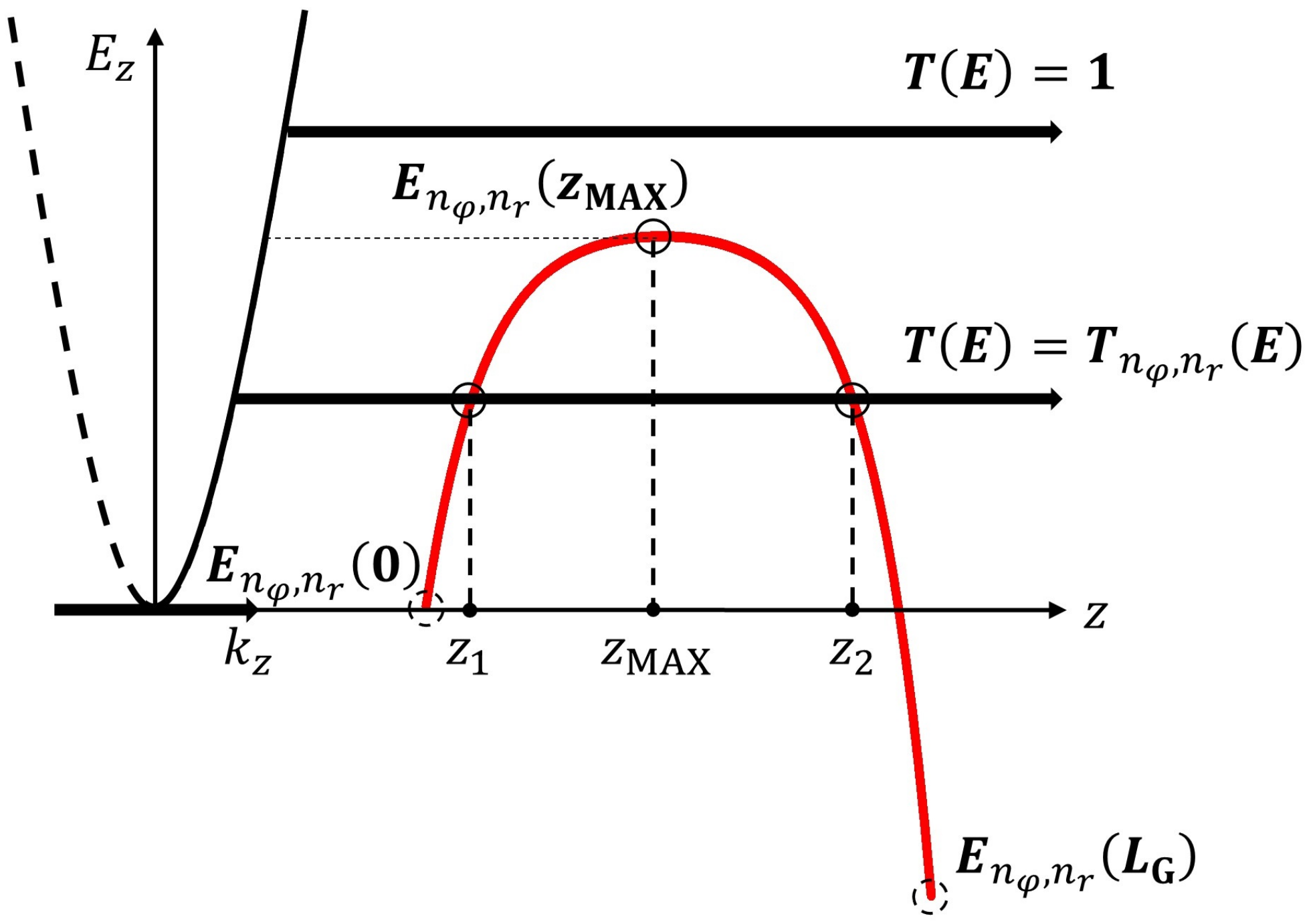
As illustrated in Figure 3, the transmission coefficient of the lowest sub-band here was unity and , corresponding to the electrons with energies higher or lower than the potential barrier top. For a high drain bias, the second term on the right-hand side of Equation (9) including could be neglected. Therefore, only the electrons injected from the source to drain could contribute to the ballistic drain current in this model. Since we could represent and in all operating regions using Equations (21) and (23), respectively, we demonstrate the drain current in all operating regions according to our previous work. Then, the formula of the drain current is as follows:

Figure 3.
Schematic representation of electrons transported between the source and drain, corresponding to their total energy. Illustrations of the quantum tunneling and thermionic ballistic transport mechanism of electron transport across the potential barrier from the source to the drain along the channel. Sub-band energy profile obtained from Equation (1) is represented. Turning points ( and ) and are shown in literal values. Here, is the electron wave vector component in the z direction corresponding to the parabolic dispersion relation for . Schematic representation for the electrons transporting between the source and drain according to the total energy of electrons. Several possible cases for electron transport are demonstrated.
4. Results and Discussion
This section compares the results from our compact model and those from a TCAD simulation using SILVACO ATLAS [49]. Numerical computations were performed on the basis of the nonequilibrium Green’s function (NEGF) formalism under the effective mass approximation coupled with Poisson’s equation. Moreover, Wolfram Mathematica software was used to present the compact model. The cylindrical coordinate was used for quasi-three-dimensional calculation, no scattering was considered, and only the lowest sub-band was taken into account. The supply voltage was set to be 0.5 V following IRDS [50], and the value was extracted from the NEGF simulation.
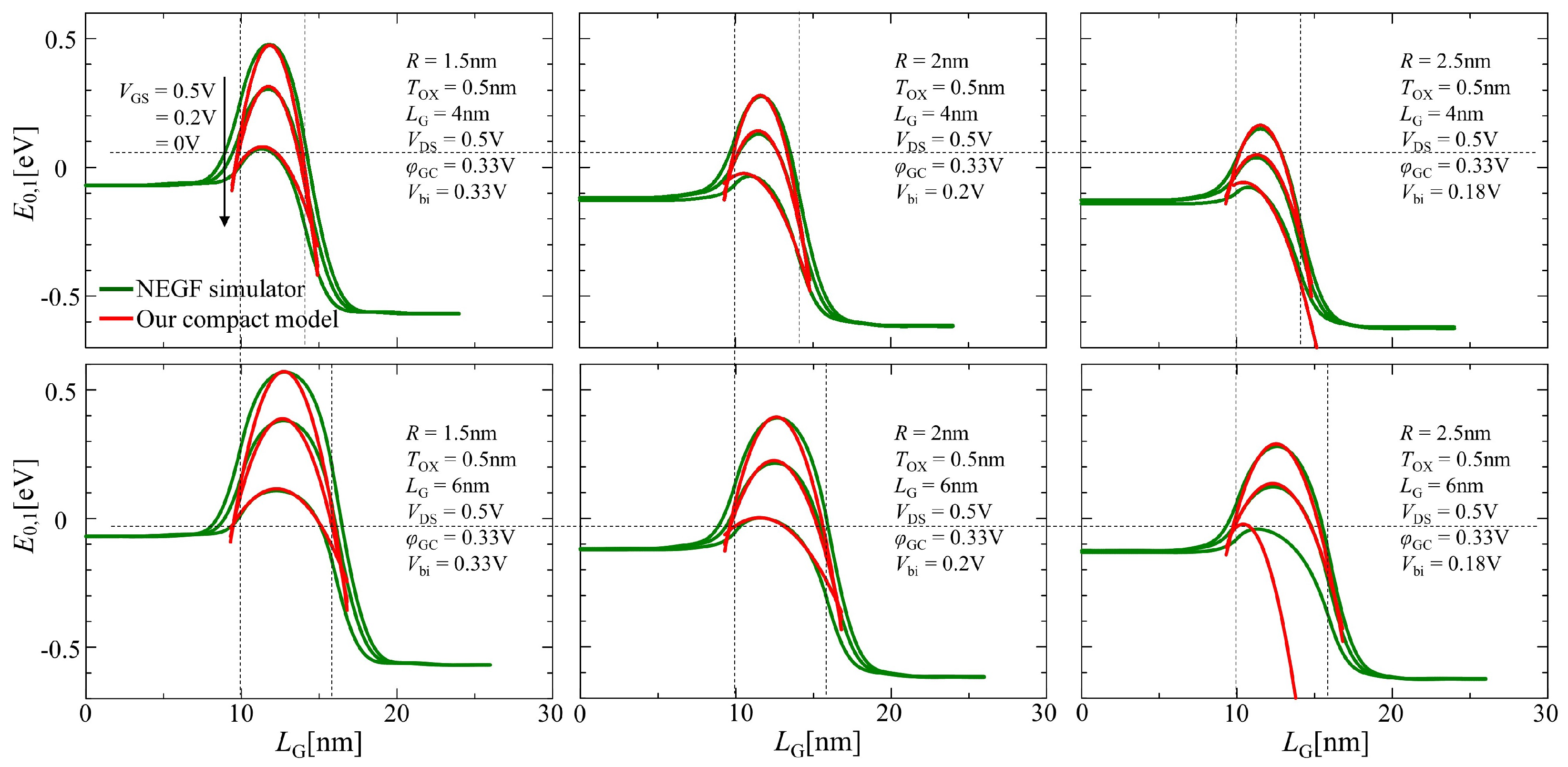
As illustrated in Figure 4, the lowest energy level profiles between the NEGF simulation and our compact model using Equation (13) were compared. Three lines correspond to the results with 0, 0.2, and 0.5 V from the top. The channel length used in this compact model was empirically expanded into the source and the drain regions by 0.5 and 1 nm throughout the comparisons between the calculations of numerical NEGF simulation and the compact model considering Equation (13) for good agreement, respectively, referring to [6].
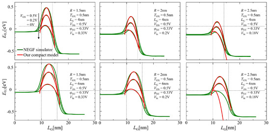
Figure 4.
Comparison of the results of the lowest sub-band profile plot between the compact model using Equation (13) and NEGF simulation under different gate bias conditions.
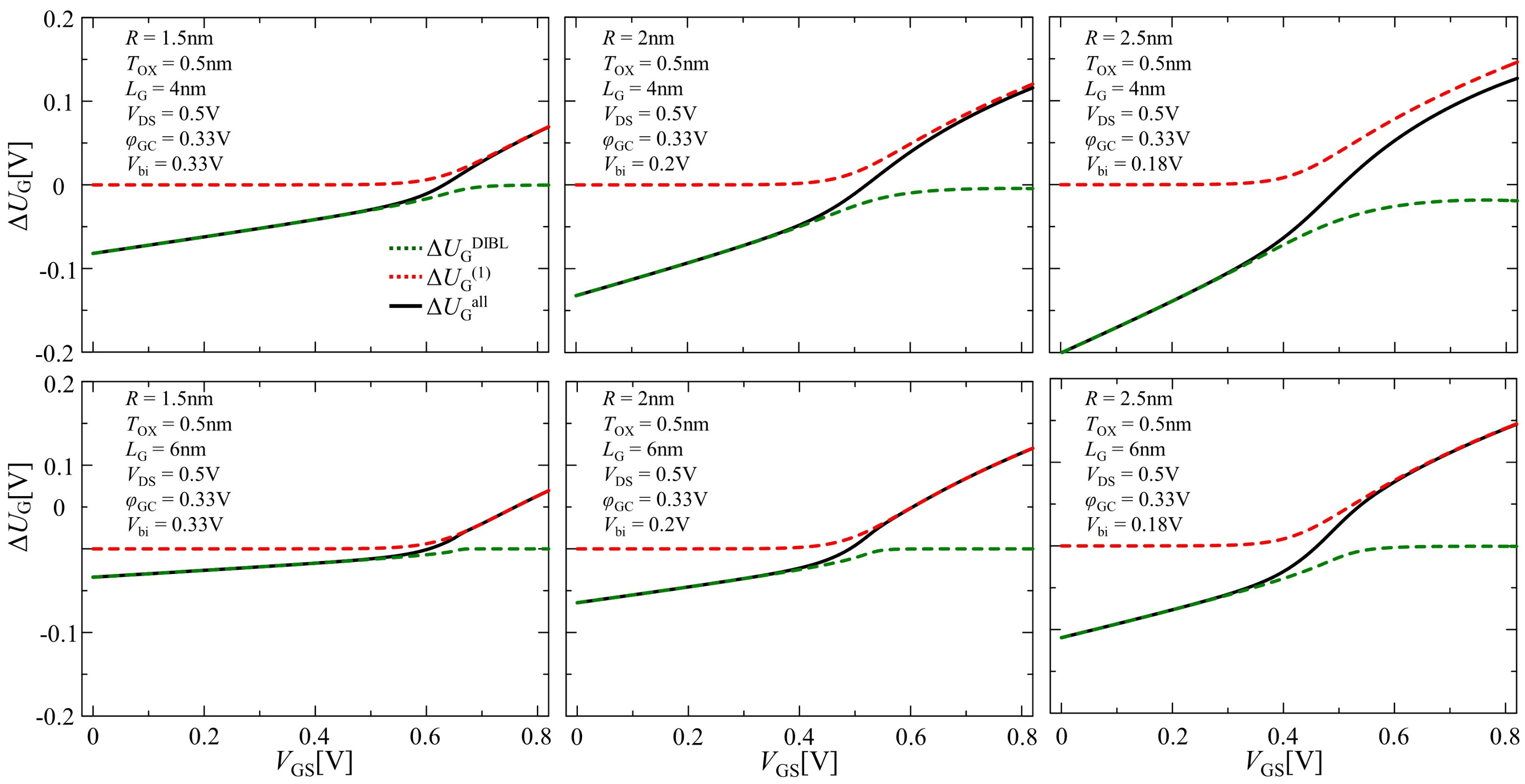
Figure 5 shows the calculation results of using a solid black line corresponding to Equation (21) in determining the unknown parameter at the barrier top for all operating regions, denoted as . The results from and , corresponding to in the subthreshold and inversion regions, are also shown as the red and green dashed lines, respectively. When the DIBL effect was neglected, in the subthreshold region was 0. On the other hand, took a negative value in the subthreshold region, while it became 0 in the inversion region deriving from Equation (20). When 2.5 nm and 4 nm, , which should have been 0 in our mentioned assumption, took a negative value, even in the inversion region. Although this case could be fixed by resetting as 2 or a greater number, an inappropriate value of affected the accuracy of the calculations for , and characteristics, as shown in the following discussion.
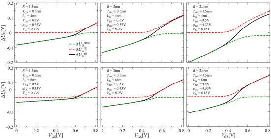
Figure 5.
Comparison of the results of , and .
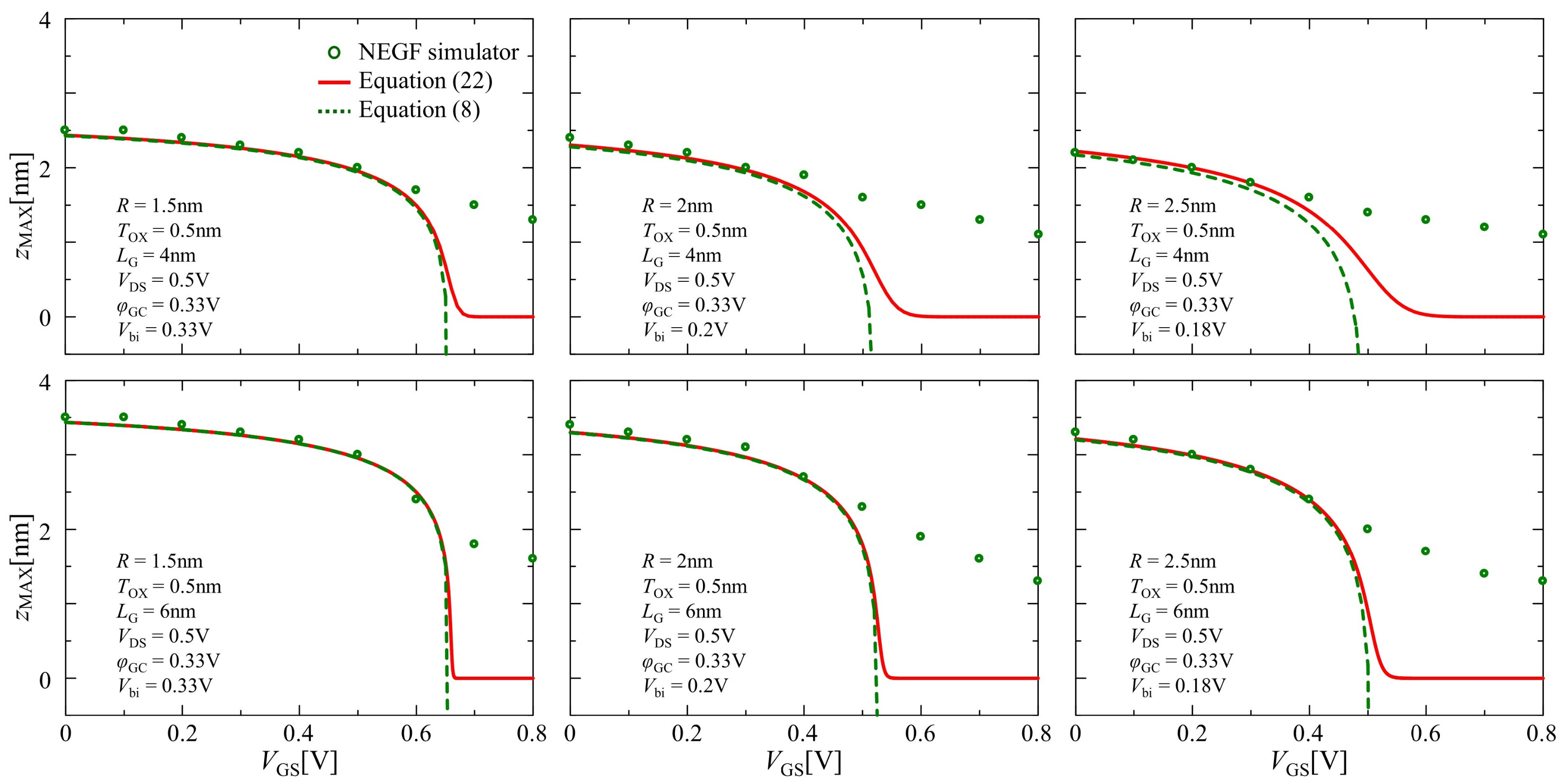
Figure 6 demonstrates comparisons of the dependencies for -, corresponding to the potential barrier top positions in the device channel at different gate voltages resulting from the NEGF simulation and our compact model. The dashed lines, solid curves, and open circles show the calculations from the compact model by using Equations (8) and (23), and the NEGF simulation, respectively. The value of calculated from (8) was valid only in the subthreshold region, and took an impossible value in the inversion region. Thereby, the necessity of deriving Equation (23) from (8), describing as a non-negative value, speaks for itself. Moreover, when exceeded 0.5 V, the compact model could not capture the results of the barrier top positions from the NEGF simulation. This limited the valid range of the operating gate bias voltage in the compact model.
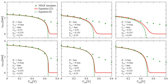
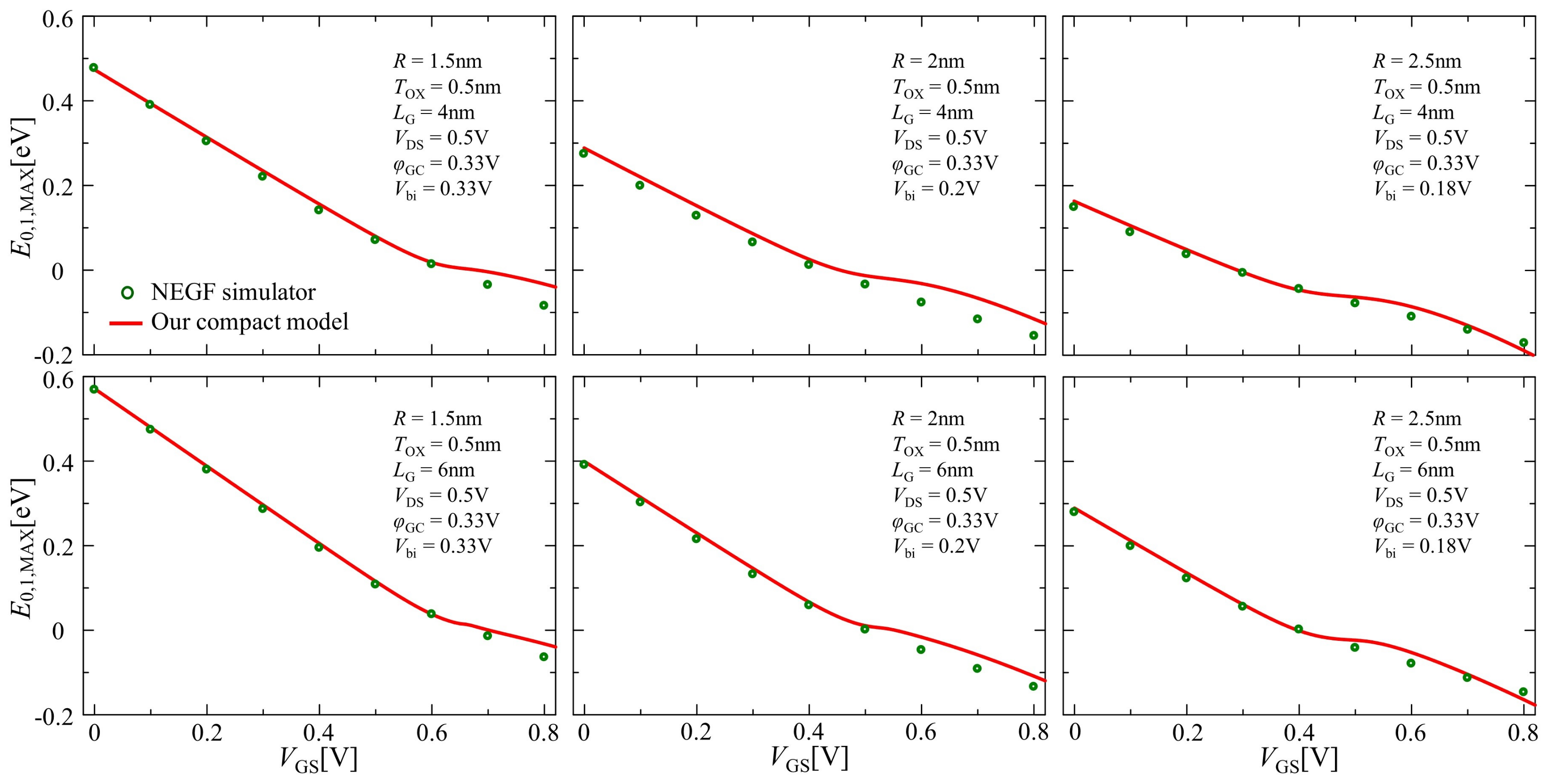
Figure 7 illustrates the gate voltage dependence of the lowest sub-band energy level at the barrier top using Equation (22). The comparisons between the NEGF simulation and our compact model with the lowest sub-band are demonstrated as open circles and solid lines, respectively, maintaining good consistency.
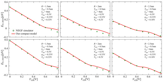
Figure 7.
Comparison of the results of the lowest sub-band energy level at the barrier top between NEGF simulation (open circle) and our compact model (solid line) for the lowest sub-band.
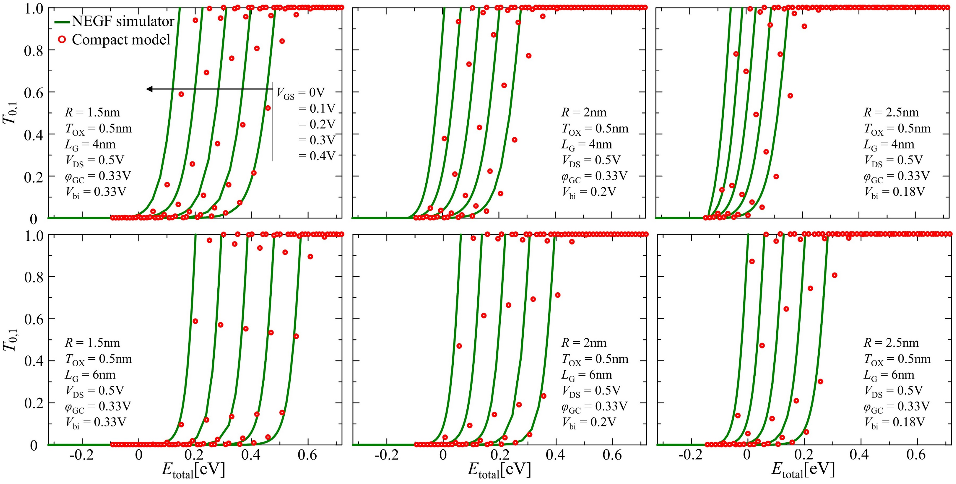
Figure 8 shows comparisons of dependencies for -, corresponding to electrons having the total energy of , between our numerical compact model using Equation (27) and NEGF simulator calculations. The open circles and solid lines relate to the calculations from the compact model and the NEGF simulation, respectively, demonstrating reasonable agreement between these results at each gate voltage level, from 0 to 0.4 V in 0.1 V steps.
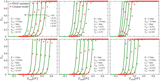
Figure 8.
Comparison of the transmission coefficient calculations results between the NEGF simulation (solid line) and our numerical compact model (open circle) for the lowest sub-band.
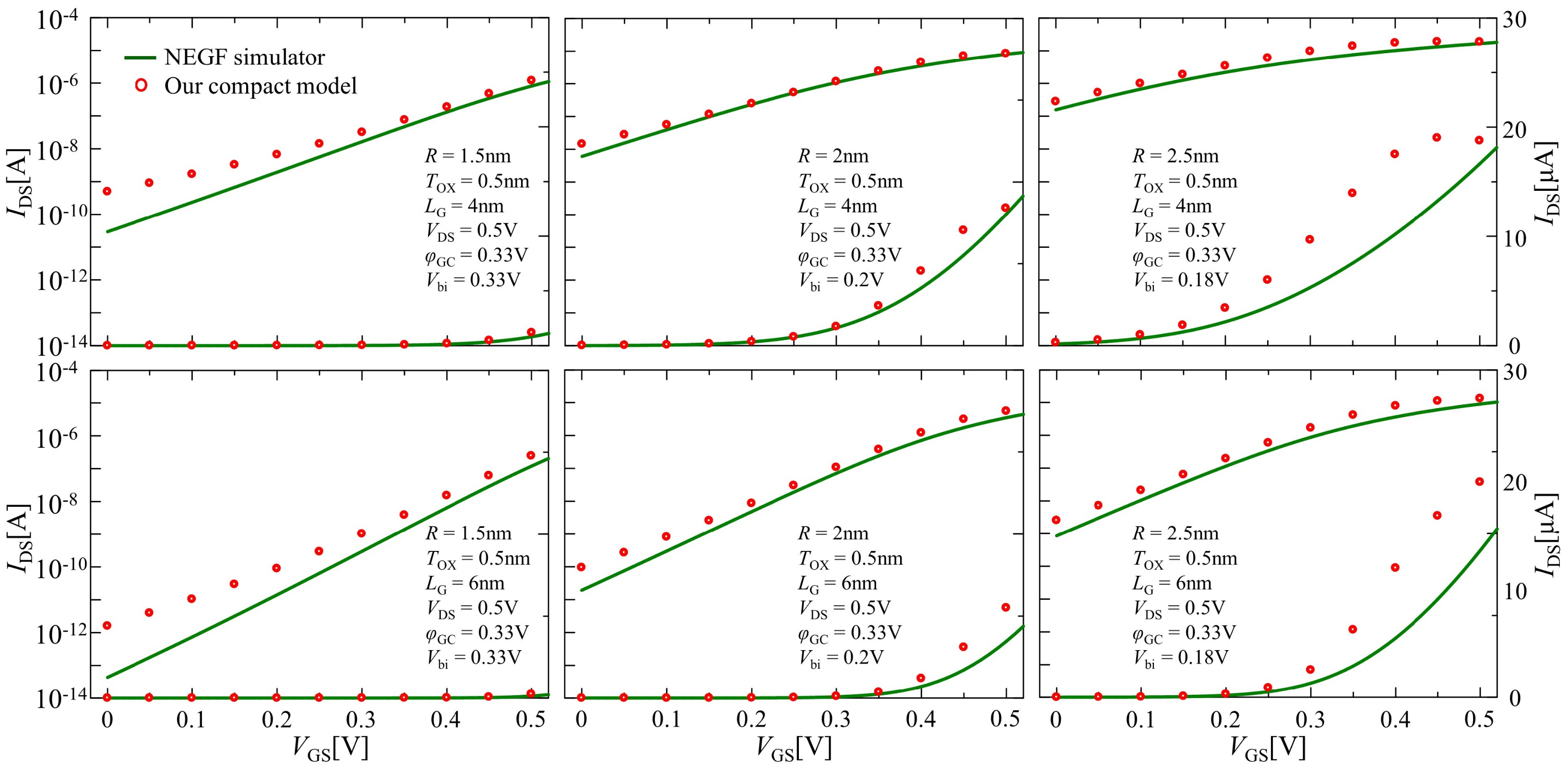
Figure 9 illustrates the drain current versus gate voltage characteristics calculated at various sets of the channel lengths and wire radius by considering Equation (28) in all operating regions. The open circle and solid line represent the comparison results of the compact model and NEGF simulation calculation, respectively. As shown in this figure, our compact model could capture the drain current increase caused by the source-to-drain tunneling in the subthreshold region while maintaining acceptable accuracy in on-current characteristics. This model was not valid when the sub-band energy level at the barrier top was lower than that at the source, which determined the maximal value of the gate voltage bias to sustain the validity of the model by solving using Equations (16) and (17). In our computations, these gate bias voltages were larger than the given supply voltage. Nevertheless, in order to obtain reasonable agreement for all operating regions, the diameter and length values of the channel needed to meet a ratio of less than unity ( < 1) in this study through their comparisons between the NEGF simulator and our compact model. Furthermore, the tunneling current should also be considered in the inversion region.
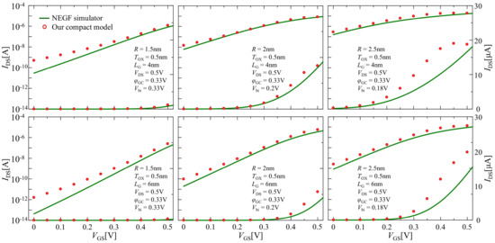
Figure 9.
Comparison results between the compact model (open circle) considering the Landauer formula and NEGF simulation (solid line) for drain current characteristic calculations in all operating regions.
5. Conclusions
This paper presented a new approach to express the numerical compact model of the drain current in the ultrashort channel nanowire GAA MOSFET using the Landauer formula. Assuming that a parabolic function could approximately determine the potential distribution along the ultrashort channel, the WKB approximation was capable of evaluating the transmission coefficients for source-to-drain tunneling. In addition, it could approximately evaluate the position of the potential barrier top and the transmission coefficient for all operating regions by using smoothing functions. Lastly, the drain current characteristics could be calculated for all operating regions. This numerical compact model was tested with a NEGF simulation, demonstrating reasonable agreement in all operating regions. Although the compact model contained several empirical parameters, they were fixed throughout the comparisons. However, a compact model with fully analytic expressions is expected to be developed to carry out a circuit simulation in a future study.
Author Contributions
Conceptualization, H.C.; Data curation, H.C. and J.W.; Formal analysis, H.C.; Funding acquisition, H.C. and Z.Y.; Investigation, H.C. and C.Z.; Methodology, H.C., C.X. and Z.Z.; Project administration, H.C. and T.L.; Resources, C.X. and Z.Z.; Software, H.C. and J.W.; Supervision, Z.Y.; Validation, H.C. and C.Z.; Visualization, H.C. and T.L.; Writing-original draft, H.C.; Writing-review & editing, H.C. All authors have read and agreed to the published version of the manuscript.
Funding
This research was funded by the Youth Innovation Promotion Association of the Chinese Academy of Sciences.
Acknowledgments
The authors would like to thank S. Uno for his inspiration to this work. This work was financially supported by the Youth Innovation Promotion Association of the Chinese Academy of Sciences (2021), no. 2021198.
Conflicts of Interest
The authors declare no conflict of interest.
References
- Rathee, D.S.; Yadav, R.; Ahuja, K. Reduction of drain induced barrier lowering by optimization Trimetal-GAA -Si -NW MOSFET in multimedia tools. Multimed. Tools Appl. 2022, 81, 19849–19862. [Google Scholar] [CrossRef]
- Bhol, K.; Nanda, U. Nanowire Array-based MOSFET for Future CMOS Technology to Attain the Ultimate Scaling Limit. Silicon 2021, 14, 1169–1177. [Google Scholar] [CrossRef]
- Kumar, R.; Bala, S.; Kumar, A. Study and Analysis of Advanced 3D Multi-Gate Junctionless Transistors. Silicon 2021, 14, 1053–1067. [Google Scholar] [CrossRef]
- Lee, Y.; Park, G.-H.; Choi, B.; Yoon, J.; Kim, H.-J.; Kim, D.H.; Kim, D.M.; Kang, M.-H.; Choi, S.-J. Design study of the gate-all-around silicon nanosheet MOSFETs. Semicond. Sci. Technol. 2020, 35, 03LT01. [Google Scholar] [CrossRef]
- Yilmaz, K.; Darbandy, G.; Reimbold, G.; Iniguez, B.; Lime, F.; Kloes, A. Equivalent DG Dimensions Concept for Compact Modeling of Short-Channel and Thin Body GAA MOSFETs Including Quantum Confinement. IEEE Trans. Electron Devices 2020, 67, 5381–5387. [Google Scholar] [CrossRef]
- Cheng, H.; Uno, S.; Nakazato, K. Analytic compact model of ballistic and quasi-ballistic transport for cylindrical gate-all-around MOSFET including drain-induced barrier lowering effect. J. Comput. Electron 2014, 14, 321–328. [Google Scholar] [CrossRef]
- Naveh, Y.; Likharev, K.K. Modeling of 10-nm-Scale Ballistic MOSFET’s. IEEE Electron Device Lett. 2000, 21, 5. [Google Scholar] [CrossRef]
- Abdi, M.A.; Djeffal, F.; Arar, D.; Hafiane, M.L. Numerical analysis of double gate and gate all around MOSFETs with bulk trap states. J. Mater. Sci. Mater. Electron. 2008, 19, 248–253. [Google Scholar] [CrossRef]
- Hosseini, R.; Fathipour, M.; Faez, R. Quantum simulation study of gate-all-around (GAA) silicon nanowire transistor and double gate metal oxide semiconductor field effect transistor (DG MOSFET). Int. J. Phys. Sci. 2012, 7, 5054–5061. [Google Scholar] [CrossRef]
- Vashishtha, V.; Clark, L.T. Comparing bulk-Si FinFET and gate-all-around FETs for the 5 nm technology node. Microelectron. J. 2021, 107, 104942. [Google Scholar] [CrossRef]
- Yilmaz, K.; Iniguez, B.; Lime, F.; Kloes, A. Quasi-Compact Model of Direct Source-to-Drain Tunneling Current in Ultrashort-Channel Nanosheet MOSFETs by Wavelet Transform. IEEE Trans. Electron. Devices 2022, 69, 1. [Google Scholar] [CrossRef]
- Zhang, Y.N.; Han, K.; Li, J.W. A Simulation Study of a Gate-All-Around Nanowire Transistor with a Core–Insulator. Micromachines 2020, 11, 223. [Google Scholar] [CrossRef] [PubMed]
- Liu, R.H.; Li, X.J.; Sun, Y.B.; Shi, Y.L. A Vertical Combo Spacer to Optimize Electrothermal Characteristics of 7-nm Nanosheet Gate-All-Around Transistor. IEEE Trans. Electron Devices 2020, 67, 1–6. [Google Scholar] [CrossRef]
- Ganapati, R.; Samoju, V.R.; Jammu, B.R. Analytical Modeling of Threshold Voltage for Dual-Metal Double-Gate Gate-All-Around (DM-DG-GAA) MOSFET. Silicon 2021, 13, 2869–2880. [Google Scholar] [CrossRef]
- Das, U.K.; Bhattacharyya, T.K. Opportunities in Device Scaling for 3-nm Node and Beyond: FinFET versus GAA-FET Versus UFET. IEEE Trans. Electron Devices 2020, 67, 2633–2638. [Google Scholar] [CrossRef]
- Jang, D.; Yakimets, D.; Eneman, G.; Schuddinck, P.; Bardon, M.G.; Raghavan, P.; Spessot, A.; Verkest, D.; Mocuta, A. Device Exploration of NanoSheet Transistors for Sub-7-nm Technology Node. IEEE Trans. Electron Devices 2017, 64, 2707–2713. [Google Scholar] [CrossRef]
- Ajayan, J.; Nirmal, D.; Tayal, S.; Bhattacharya, S.; Arivazhagan, L.; Augustine Fletcher, A.A.S.; Murugapandiyan, P.; Ajitha, D. Nanosheet field effect transistors—A next generation device to keep Moore’s law alive: An intensive study. Microelectron. J. 2021, 114, 105141. [Google Scholar] [CrossRef]
- Natori, K. Ballistic/quasi-ballistic transport in nanoscale transistor. Appl. Surf. Sci. 2008, 254, 6194–6198. [Google Scholar] [CrossRef]
- Gu, J.; Zhang, Q.; Wu, Z.; Yao, J.; Zhang, Z.; Zhu, X.; Wang, G.; Li, J.; Zhang, Y.; Cai, Y. Cryogenic Transport Characteristics of P-Type Gate-All-Around Silicon Nanowire MOSFETs. Nanomaterials 2021, 11, 309. [Google Scholar] [CrossRef]
- Chatterjee, A.K.; Kushwaha, M.; Prasad, B. Analytical Model for Drain Current of a Ballistic MOSFET. Silicon 2021, 13, 1777–1785. [Google Scholar] [CrossRef]
- Aguirre, P.; Schenk, A. Ballistic Mobility Model for QDD Simulation of Ultra-short Transistors. In Proceedings of the 2018 IEEE 2nd Electron Devices Technology and Manufacturing Conference (EDTM), Kobe, Japan, 13–16 March 2018; pp. 77–79. [Google Scholar] [CrossRef]
- Cheng, H.; Zhang, C.; Liu, T.F.; Xie, C.; Yang, Z.J.; Zhang, Z.P. A Charge Density Model of Silicon-nanowire GAA MOSFET Incoroperating the Source-drian Tunneling Effect for IC Design. In Proceedings of the 2021 International Symposium on Computer Technology and Information Science (ISCTIS), Guilin, China, 4–6 June 2021; pp. 351–355. [Google Scholar] [CrossRef]
- Cousin, B.; Reyboz, M.; Rozeau, O.; Jaud, M.A.; Ernst, T.; Jomaah, J. A unified short-channel compact model for cylindrical surrounding-gate MOSFET. Solid-State Electron. 2011, 56, 40–46. [Google Scholar] [CrossRef]
- Cheng, H.; Uno, S.; Numata, T.; Nakazato, K. Analytic Compact Model of Ballistic and Quasi-Ballistic Cylindrical Gate-All-Around Metal-Oxide-Semiconductor Field Effect Transistors Including Two Subbands. Jpn. J. Appl. Phys. 2013, 52, 04CN03. [Google Scholar] [CrossRef]
- Cheng, H.; Zhang, Z.; Yang, Z.; Liu, Z. Compact model of short-channel cylindrical ballistic gate-all-around mosfet including the source-to-drain tunneling. J. Phys. Conf. Ser. 2018, 1026, 012011. [Google Scholar] [CrossRef]
- Mohan, C.; Choudhary, S.; Prasad, B. Gate All Around FET: AnAlternative of FinFET for Future Technology Nodes. In Proceedings of the International Conference on Emerging Trends in Engineering, Technology, Science and Management ICETETSM-2017, New Delhi, India, 11 June 2017; pp. 561–569. [Google Scholar]
- Yoon, J.S.; Jeong, J.; Lee, S.; Lee, J.; Baek, R.H. Gate-all-around FETs–nanosheet structure. In Nanowires–Recent Progress; IntechOpen: Rijeka, Croatia, 2020; Chapter 9. [Google Scholar] [CrossRef]
- Darbandy, G.; Mothes, S.; Schröter, M.; Kloes, A.; Claus, M. Performance analysis of parallel array of nanowires and a nanosheet in SG, DG and GAA FETs. Solid-State Electron. 2019, 162, 107641. [Google Scholar] [CrossRef]
- Kim, S.; Lee, K.; Kim, S.; Kim, M.; Lee, J.H.; Kim, S.; Park, B.G. Investigation of Device Performance for Fin Angle Optimization in FinFET and Gate-All-Around FETs for 3 nm-Node and Beyond. IEEE Trans. Electron Devices 2022, 69, 2088–2093. [Google Scholar] [CrossRef]
- Mil’nikov, G.; Mori, N.; Kamakura, Y.; Ezaki, T. R-matrix theory of quantum transport and recursive propagation method for device simulations. J. Appl. Phys. 2008, 104, 044506. [Google Scholar] [CrossRef]
- Khan, T.; Iztihad, H.M.; Sufian, A.; Alam, M.N.K.; Mollah, M.N.; Islam, M.R. Gate length scaling of Si nanowire FET: A NEGF study. In Proceedings of the 2015 International Conference on Electrical Engineering and Information Communication Technology (ICEEICT), Savar, Bangladesh, 21–23 May 2015; pp. 1–4. [Google Scholar] [CrossRef]
- Zeng, J.W.; Deng, W.L.; Zhou, C.J.; Peng, J.; Huang, J.K. A Compact Model of MoS2 Field-Effect Transistors From Drift-Diffusion to Ballistic Carrier Transport Regimes. IEEE J. Electron Dev. 2020, 8, 285–290. [Google Scholar] [CrossRef]
- Vimala, P.; Kumar, N.R.N. Analytical Quantum Model for Germanium Channel Gate-All-Around (GAA) MOSFET. J. Nano Res. 2019, 59, 137–148. [Google Scholar] [CrossRef]
- Kim, S.; Kim, J.; Jang, D.; Ritzenthaler, R.; Lee, J.W. Comparison of temperature dependent carrier transport in finfet and gate-all-around nanowire fet. Appl. Sci. 2020, 10, 2979. [Google Scholar] [CrossRef]
- Bhol, K.; Jena, B.; Nanda, U. Journey of MOSFET from Planar to Gate All Around: A Review. Recent Pat. Nanotechnol. 2022, 16, 326–332. [Google Scholar] [CrossRef]
- Natori, K.; Kimura, Y.; Shimizu, T. Characteristics of a carbon nanotube field-effect transistor analyzed as a ballistic nanowire field-effect transistor. J. Appl. Phys. 2005, 97, 034306. [Google Scholar] [CrossRef]
- Hamid, H.A.E.; Iñíguez, B.; Guitart, J.R. Analytical model of the threshold voltage and subthreshold swing of undoped cylindrical gate-all-around-based MOSFETs. IEEE Trans. Electron Devices 2007, 54, 572–579. [Google Scholar] [CrossRef]
- Ragi, R.; Tayette da Nobrega, R.V.; Duarte, U.R.; Romero, M.A. An explicit quantum-mechanical compact model for the I–Vcharacteristics of cylindrical nanowire MOSFETs. IEEE Trans. Nanotechnol. 2016, 15, 627–634. [Google Scholar] [CrossRef]
- Seon, Y.; Kim, J.; Kim, S.; Jeon, J. Analytical Current-Voltage Model for Gate-All-Around Transistor with Poly-Crystalline Silicon Channel. Electronics 2019, 8, 988. [Google Scholar] [CrossRef]
- Numata, T.; Uno, S.; Hattori, J.; Mil’Nikov, G.; Kamakura, Y.; Mori, N.; Nakazato, K. A Self-Consistent Compact Model of Ballistic Nanowire MOSFET with Rectangular Cross Section. IEEE Trans. Electron. Devices 2013, 60, 856–862. [Google Scholar] [CrossRef]
- Lin, Y.K.; Duarte, J.P.; Kushwaha, P.; Agarwal, H.; Chang, H.L.; Sachid, A.; Salahuddin, S.; Hu, C.M. Compact Modeling Source-to-Drain Tunneling in Sub-10-nm GAA FinFET With Industry Standard Model. IEEE Trans. Electron Devices 2017, 64, 3576–3581. [Google Scholar] [CrossRef]
- Zhang, X.Y.; Lam, K.T.; Low, K.L.; Yeo, Y.C.; Liang, G.C. Nanoscale FETs Simulation Based on Full-Complex-Band Structure and Self-Consistently Solved Atomic Potential. IEEE Trans. Electron Devices 2017, 64, 58–65. [Google Scholar] [CrossRef]
- Wong, H. Compact Modeling and Short-Channel Effects of Nanowire MOS Transistors. In Proceedings of the 2018 IEEE International Conference on Integrated Circuits, Technologies and Applications (ICTA), Beijing, China, 21–23 November 2018; pp. 7–10. [Google Scholar] [CrossRef]
- Lee, K.H.; Erlebach, A.; Penzin, O.; Smith, L. Quasi-Ballistic Drift-Diffusion Simulation of SiGe Nanowire MOSFETs Using the Kinetic Velocity Model. J. Electron Devices Soc. 2021, 9, 387–392. [Google Scholar] [CrossRef]
- Dasgupta, A.; Parihar, S.S.; Kushwaha, P.; Agarwal, H.; Kao, M.Y.; Salahuddin, S.; Chauhan, Y.S.; Hu, C.M. BSIM Compact Model of Quantum Confinement in Advanced Nanosheet FETs. IEEE Trans. Electron Devices 2020, 67, 730–737. [Google Scholar] [CrossRef]
- Bae, M.S.; Park, C.; Yun, H. Compact Drain Current Model of Nanoscale FinFET Considering Short Channel Effect in Ballistic Transport Regime. In Proceedings of the 2018 15th International Conference on Synthesis, Modeling, Analysis and Simulation Methods and Applications to Circuit Design (SMACD), Prague, Czech Republic, 2–5 July 2018; pp. 109–112. [Google Scholar] [CrossRef]
- Cheng, H.; Liu, T.F.; Zhang, C.; Liu, Z.F.; Yang, Z.J.; Nakazato, K.; Zhang, Z.P. Nanowire gate-all-around MOSFETs modeling: Ballistic transport incorporating the source-to-drain tunneling. Jpn. J. Appl. Phys. 2020, 59, 074002. [Google Scholar] [CrossRef]
- Numata, T.; Uno, S.; Kamakura, Y.; Mori, N.; Nakazato, K. Analytic Circuit Model of Ballistic Nanowire Metal–Oxide–Semiconductor Field-Effect Transistor for Transient Analysis. Jpn. J. Appl. Phys. 2013, 52, 04CN01. [Google Scholar] [CrossRef]
- Atlas User’s Manual DEVICE SIMULATION SOFTWARE, Charpter 14, Quantum Effect Simulation. Silvaco, Inc.: Santa Clara, CA, USA, 2016; pp. 771–815. Available online: https://dynamic.silvaco.com/dynamicweb/silen/ (accessed on 25 September 2022).
- More Moore. International Roadmap for Devices and Systems: 2017 Edition. IEEE Advancing Technology for Humanity. 2017. Available online: https://irds.ieee.org/editions/2017 (accessed on 25 September 2022).
Publisher’s Note: MDPI stays neutral with regard to jurisdictional claims in published maps and institutional affiliations. |
© 2022 by the authors. Licensee MDPI, Basel, Switzerland. This article is an open access article distributed under the terms and conditions of the Creative Commons Attribution (CC BY) license (https://creativecommons.org/licenses/by/4.0/).

