
The Light Absorption Enhancement in Graphene Monolayer Resulting from the Diffraction Coupling of Surface Plasmon Polariton Resonance

 ,
, 
Abstract
:1. Introduction
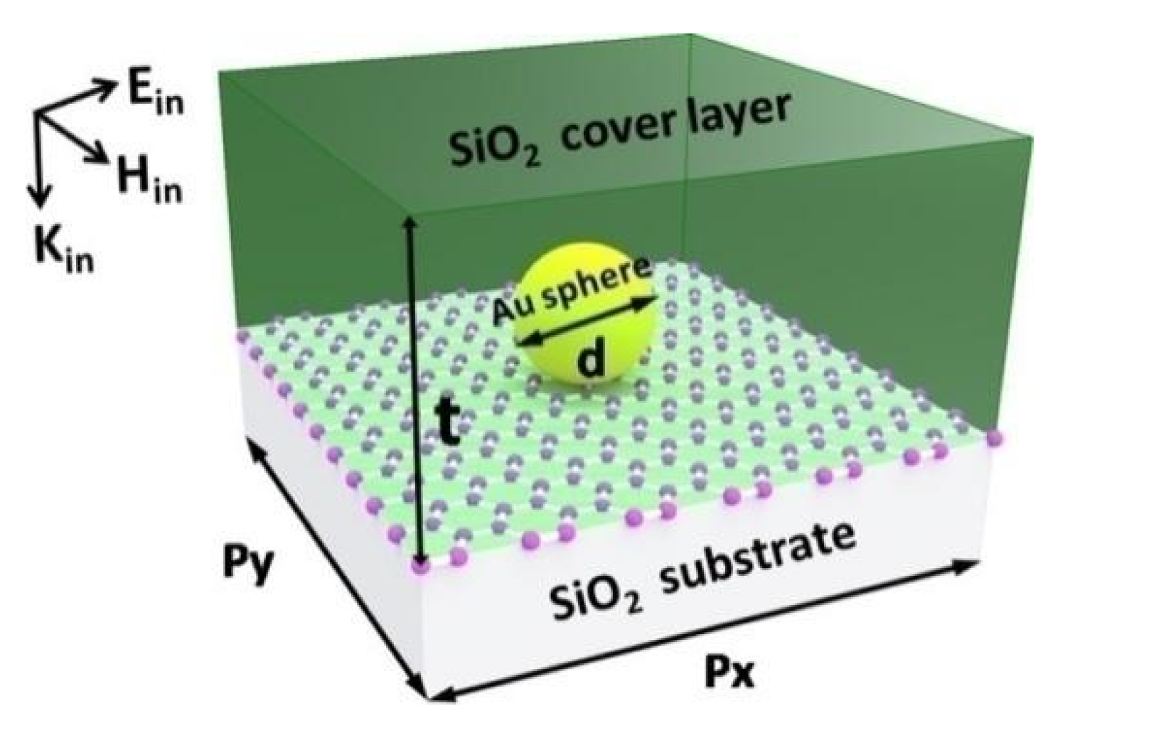
2. Methods
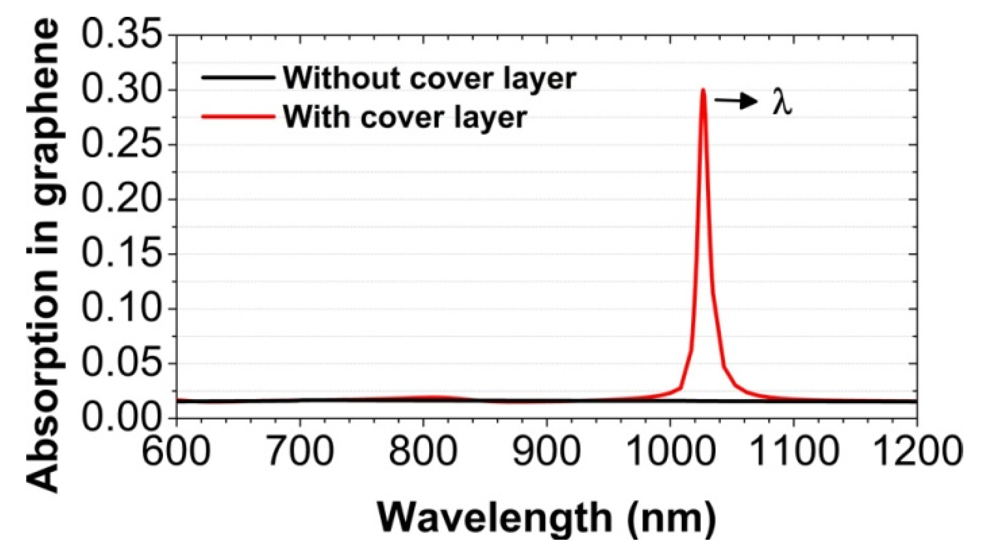
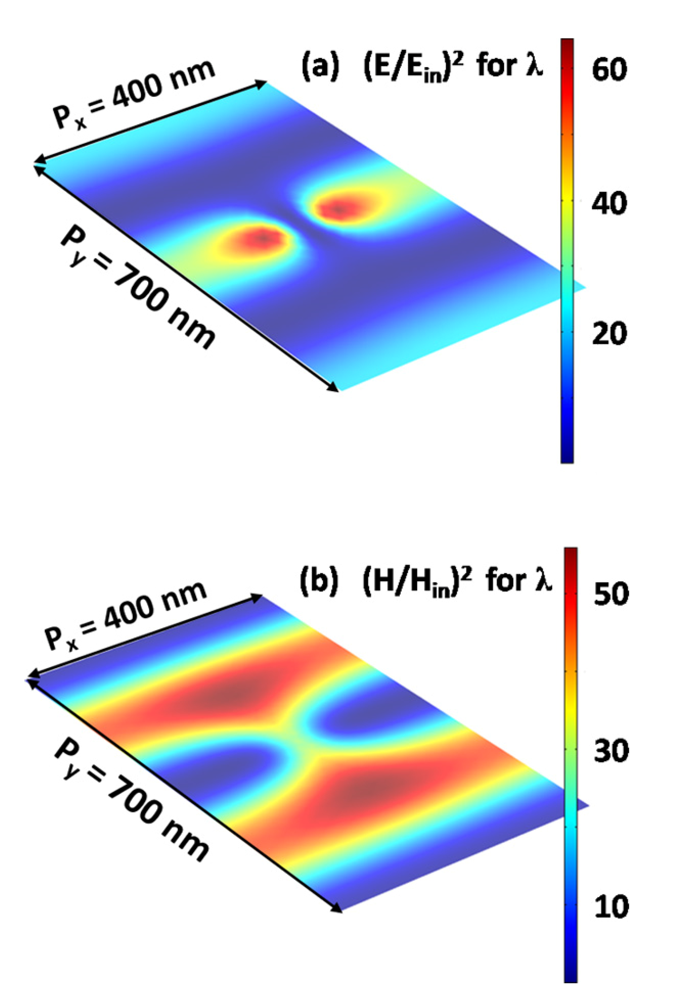
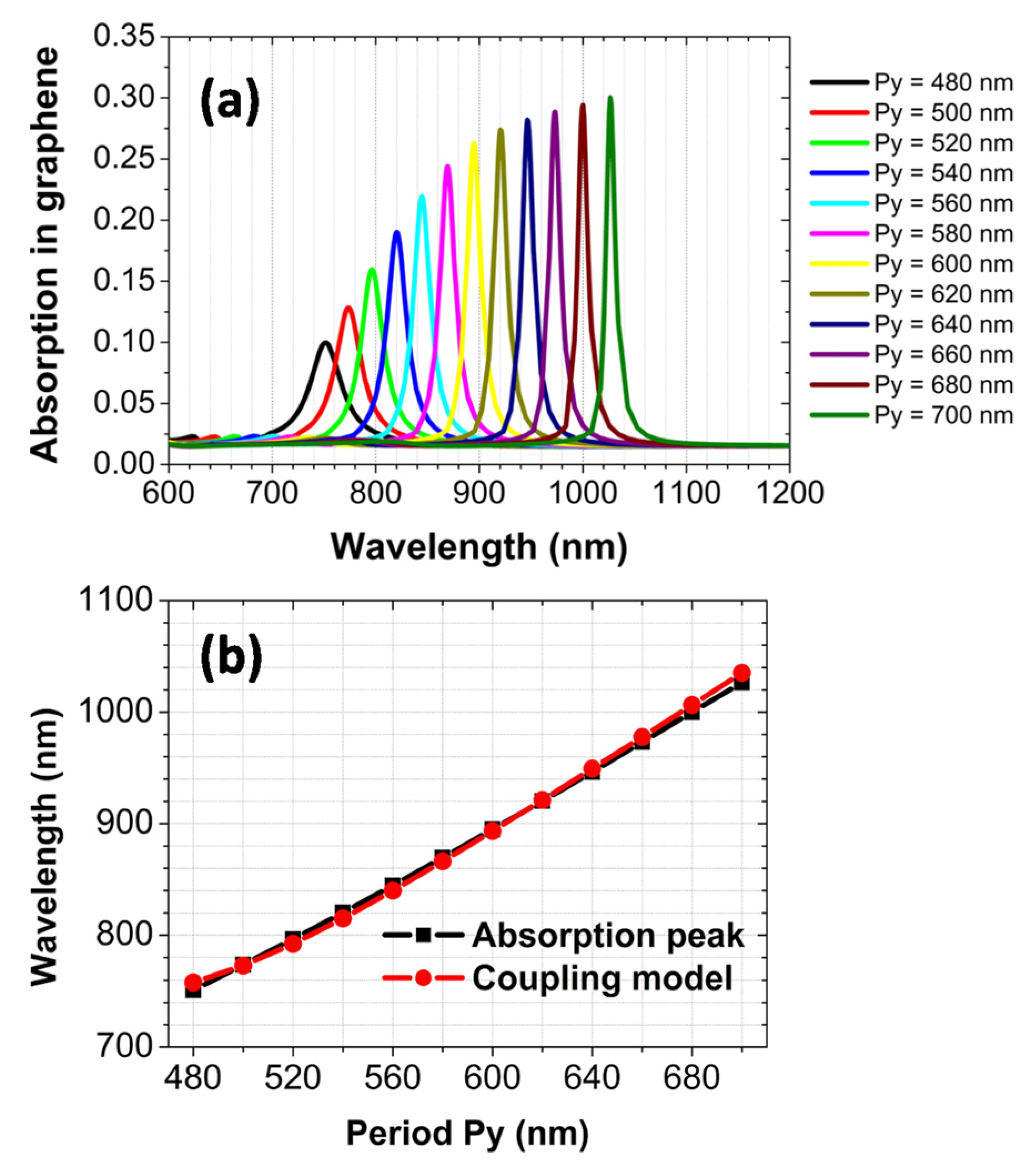
3. Results and Discussion
4. Conclusions
Author Contributions
Funding
Institutional Review Board Statement
Informed Consent Statement
Data Availability Statement
Conflicts of Interest
References
- Nair, R.R.; Blake, P.; Grigorenko, A.N.; Novoselov, K.S.; Booth, T.J.; Stauber, T.; Peres, N.M.R.; Geim, A.K. Fine Structure Constant Defines Visual Transparency of Graphene. Science 2008, 320, 1308. [Google Scholar] [CrossRef] [Green Version]
- Dawlaty, J.M.; Shivaraman, S.; Strait, J.; George, P.; Chandrashekhar, M.; Rana, F.; Spencer, M.G.; Veksler, D.; Chen, Y. Measurement of the optical absorption spectra of epitaxial graphene from terahertz to visible. Appl. Phys. Lett. 2008, 93, 131905. [Google Scholar] [CrossRef] [Green Version]
- Ferrari, A.C.; Bonaccorso, F.; Fal’ko, V.; Novoselov, K.S.; Roche, S.; Bøggild, P.; Borini, S.; Koppens, F.H.L.; Palermo, V.; Pugno, N.; et al. Science and technology roadmap for graphene, related two-dimensional crystals, and hybrid systems. Nanoscale 2015, 7, 4598–4810. [Google Scholar] [CrossRef] [PubMed] [Green Version]
- Liu, C.-H.; Chang, Y.-C.; Norris, T.B.; Zhong, Z. Graphene photodetectors with ultra-broadband and high responsivity at room temperature. Nat. Nanotechnol. 2014, 9, 273–278. [Google Scholar] [CrossRef]
- Koppens, F.; Mueller, T.; Avouris, P.; Ferrari, A.C.; Vitiello, M.S.; Polini, M. Photodetectors based on graphene, other two-dimensional materials and hybrid systems. Nat. Nanotechnol. 2014, 9, 780–793. [Google Scholar] [CrossRef]
- Liu, Z.; Liu, Q.; Huang, Y.; Ma, Y.; Yin, S.; Zhang, X.; Sun, W.; Chen, Y. Organic Photovoltaic Devices Based on a Novel Acceptor Material: Graphene. Adv. Mater. 2008, 20, 3924–3930. [Google Scholar] [CrossRef]
- Echtermeyer, T.; Britnell, L.; Jasnos, P.K.; Lombardo, A.; Gorbachev, R.; Grigorenko, A.N.; Geim, A.K.; Ferrari, A.C.; Novoselov, K. Strong plasmonic enhancement of photovoltage in graphene. Nat. Commun. 2011, 2, 1–5. [Google Scholar] [CrossRef] [Green Version]
- Zhang, N.; Zhang, Y.; Xu, Y.-J. Recent progress on graphene-based photocatalysts: Current status and future perspectives. Nanoscale 2012, 4, 5792–5813. [Google Scholar] [CrossRef] [PubMed]
- Liu, Z.; Zhou, J.; Liu, X.; Fu, G.; Liu, G.; Tang, C.; Chen, J. High-Q plasmonic graphene absorbers for electrical switching and optical detection. Carbon 2020, 166, 256–264. [Google Scholar] [CrossRef]
- Yan, Z.; Zhu, Q.; Wan, M.; Lu, X.; Pu, X.; Tang, C.; Yu, L. Graphene ultraviolet ultrahigh-Q perfect absorption for nanoscale optical sensing. Opt. Express 2020, 28, 6095–6101. [Google Scholar] [CrossRef]
- Yan, Z.; Lu, X.; Du, W.; Lv, Z.; Tang, C.; Cai, P.; Gu, P.; Chen, J.; Yu, Z. Ultraviolet graphene ultranarrow absorption engineered by lattice plasmon resonance. Nanotechnology 2021, 32, 465202. [Google Scholar] [CrossRef]
- Teng, D.; Wang, K.; Li, Z. Graphene-Coated Nanowire Waveguides and Their Applications. Nanomaterials 2020, 10, 229. [Google Scholar] [CrossRef] [Green Version]
- Cheng, J.; Fan, F.; Chang, S. Recent Progress on Graphene-Functionalized Metasurfaces for Tunable Phase and Polarization Control. Nanomaterials 2019, 9, 398. [Google Scholar] [CrossRef] [PubMed] [Green Version]
- Nurrohman, D.; Chiu, N.-F. A Review of Graphene-Based Surface Plasmon Resonance and Surface-Enhanced Raman Scattering Biosensors: Current Status and Future Prospects. Nanomaterials 2021, 11, 216. [Google Scholar] [CrossRef] [PubMed]
- Liu, C.; Guo, J.; Yu, L.; Li, J.; Zhang, M.; Li, H.; Shi, Y.; Dai, D. Silicon/2D-material photodetectors: From near-infrared to mid-infrared. Light. Sci. Appl. 2021, 10, 1–21. [Google Scholar] [CrossRef]
- Yin, J.; Liu, L.; Zang, Y.; Ying, A.; Hui, W.; Jiang, S.; Zhang, C.; Yang, T.; Chueh, Y.-L.; Li, J.; et al. Engineered tunneling layer with enhanced impact ionization for detection improvement in graphene/silicon heterojunction photodetectors. Light. Sci. Appl. 2021, 10, 113. [Google Scholar] [CrossRef] [PubMed]
- Qin, C.; Jia, K.; Li, Q.; Tan, T.; Wang, X.; Guo, Y.; Huang, S.-W.; Liu, Y.; Zhu, S.; Xie, Z.; et al. Electrically controllable laser frequency combs in graphene-fibre microresonators. Light. Sci. Appl. 2020, 9, 185. [Google Scholar] [CrossRef]
- Zeng, B.; Huang, Z.; Singh, A.; Yao, Y.; Azad, A.K.; Mohite, A.D.; Taylor, A.J.; Smith, D.R.; Chen, H.-T. Hybrid graphene metasurfaces for high-speed mid-infrared light modulation and single-pixel imaging. Light. Sci. Appl. 2018, 7, 51. [Google Scholar] [CrossRef] [PubMed]
- Li, Q.; Lu, J.; Gupta, P.; Qiu, M. Engineering Optical Absorption in Graphene and Other 2D Materials: Advances and Applications. Adv. Opt. Mater. 2019, 7, 1900595. [Google Scholar] [CrossRef]
- Guo, C.; Zhang, J.; Xu, W.; Liu, K.; Yuan, X.; Qin, S.; Zhu, Z. Graphene-Based Perfect Absorption Structures in the Visible to Terahertz Band and Their Optoelectronics Applications. Nanomaterials 2018, 8, 1033. [Google Scholar] [CrossRef] [Green Version]
- Xiong, F.; Zhang, J.; Zhu, Z.; Yuan, X.; Qin, S. Ultrabroadband, More than One Order Absorption Enhancement in Graphene with Plasmonic Light Trapping. Sci. Rep. 2015, 5, 16998. [Google Scholar] [CrossRef] [PubMed] [Green Version]
- Niu, J.; Luo, M.; Zhu, J.; Liu, Q.H. Enhanced plasmonic light absorption engineering of graphene: Simulation by boundary-integral spectral element method. Opt. Express 2015, 23, 4539–4551. [Google Scholar] [CrossRef] [PubMed]
- Liu, B.; Tang, C.; Chen, J.; Wang, Q.; Pei, M.; Tang, H. Dual-band light absorption enhancement of monolayer graphene from surface plasmon polaritons and magnetic dipole resonances in metamaterials. Opt. Express 2017, 25, 12061. [Google Scholar] [CrossRef] [PubMed]
- Zhang, L.; Tang, L.; Wei, W.; Cheng, X.; Wang, W.; Zhang, H. Enhanced near-infrared absorption in graphene with multilayer metal-dielectric-metal nanostructure. Opt. Express 2016, 24, 20002–20009. [Google Scholar] [CrossRef] [PubMed]
- Jiang, X.; Wang, T.; Xiao, S.; Yan, X.; Cheng, L.; Le Cheng, S.X.X.Y.A. Tunable ultra-high-efficiency light absorption of monolayer graphene using critical coupling with guided resonance. Opt. Express 2017, 25, 27028. [Google Scholar] [CrossRef] [PubMed] [Green Version]
- Grande, M.; Vincenti, M.A.; Stomeo, T.; Bianco, G.V.; De Ceglia, D.; Aközbek, N.; Petruzzelli, V.; Bruno, G.; De Vittorio, M.; Scalora, M.; et al. Graphene-based absorber exploiting guided mode resonances in one-dimensional gratings. Opt. Express 2014, 22, 31511–31519. [Google Scholar] [CrossRef] [PubMed]
- Zhu, J.; Li, C.; Ou, J.-Y.; Liu, Q.H. Perfect light absorption in graphene by two unpatterned dielectric layers and potential applications. Carbon 2019, 142, 430–437. [Google Scholar] [CrossRef] [Green Version]
- Ye, Q.; Wang, J.; Liu, Z.; Deng, Z.-C.; Kong, X.-T.; Xing, F.; Chen, X.-D.; Zhou, W.-Y.; Zhang, C.-P.; Tian, J.-G. Polarization-dependent optical absorption of graphene under total internal reflection. Appl. Phys. Lett. 2013, 102, 021912. [Google Scholar] [CrossRef]
- Wang, Z.; Hou, Y.; Hou, Z.W.A.Y. Ultra-multiband absorption enhancement of graphene in a metal-dielectric-graphene sandwich structure covering terahertz to mid-infrared regime. Opt. Express 2017, 25, 19185–19194. [Google Scholar] [CrossRef]
- Zhou, K.; Cheng, Q.; Song, J.; Lu, L.; Luo, Z. Highly efficient narrow-band absorption of a graphene-based Fabry-Perot structure at telecommunication wavelengths. Opt. Lett. 2019, 44, 3430–3433. [Google Scholar] [CrossRef]
- Yang, Q.; Zhang, C.; Wu, S.; Li, S.; Bao, Q.; Giannini, V.; Maier, S.A.; Li, X. Photonic surface waves enabled perfect infrared absorption by monolayer graphene. Nano Energy 2018, 48, 161–169. [Google Scholar] [CrossRef]
- Liu, J.; Liu, N.-H.; Li, J.; Li, X.J.; Huang, J.-H. Enhanced absorption of graphene with one-dimensional photonic crystal. Appl. Phys. Lett. 2012, 101, 052104. [Google Scholar] [CrossRef]
- Liu, B.; Yu, W.; Yan, Z.; Tang, C.; Chen, J.; Gu, P.; Liu, Z.; Huang, Z. Ultra-narrowband light absorption enhancement of monolayer graphene from waveguide mode. Opt. Express 2020, 28, 24908. [Google Scholar] [CrossRef]
- Xiong, F.; Zhou, J.; Xu, W.; Zhu, Z.; Yuan, X.; Zhang, J.; Qin, S. Visible to near-infrared coherent perfect absorption in monolayer graphene. J. Opt. 2018, 20, 095401. [Google Scholar] [CrossRef]
- Zhao, C.-X.; Qie, Y.; Yu, Y.; Ma, R.-R.; Qin, J.-F.; Liu, Y. Enhanced optical absorption of graphene by plasmon. Acta Phys. Sin. 2020, 69, 067801. [Google Scholar] [CrossRef]
- Tang, L.; Shi, H.; Yang, J.; Du, C.; Gao, F.; Zhu, J.; Du, J. Complete optical absorption in graphene by using nano-gratings to excite graphene surface plasmons. Microelectron. Eng. 2015, 145, 58–61. [Google Scholar] [CrossRef]
- Yektaparast, B.; Shirkani, H. Controlling Optical Absorption of Graphene in Near-infrared Region by Surface Plasmons. Plasmonics 2018, 13, 1623–1630. [Google Scholar] [CrossRef]
- Zou, S.; Janel, N.; Schatz, G.C. Silver nanoparticle array structures that produce remarkably narrow plasmon lineshapes. J. Chem. Phys. 2004, 120, 10871–10875. [Google Scholar] [CrossRef]
- Zou, S.; Schatz, G.C. Narrow plasmonic/photonic extinction and scattering line shapes for one and two dimensional silver nanoparticle arrays. J. Chem. Phys. 2004, 121, 12606–12612. [Google Scholar] [CrossRef]
- Kravets, V.G.; Schedin, F.; Grigorenko, A.N. Extremely Narrow Plasmon Resonances Based on Diffraction Coupling of Localized Plasmons in Arrays of Metallic Nanoparticles. Phys. Rev. Lett. 2008, 101, 087403. [Google Scholar] [CrossRef]
- Auguié, B.; Barnes, W.L. Collective Resonances in Gold Nanoparticle Arrays. Phys. Rev. Lett. 2008, 101, 143902. [Google Scholar] [CrossRef] [Green Version]
- de Abajo, F.J.G. Colloquium: Light scattering by particle and hole arrays. Rev. Mod. Phys. 2007, 79, 1267–1290. [Google Scholar] [CrossRef] [Green Version]
- Kravets, V.G.; Kabashin, A.V.; Barnes, W.L.; Grigorenko, A.N. Plasmonic Surface Lattice Resonances: A Review of Properties and Applications. Chem. Rev. 2018, 118, 5912–5951. [Google Scholar] [CrossRef]
- Auguié, B.; Bendaña, X.M.; Barnes, W.L.; de Abajo, F.J.G. Diffractive arrays of gold nanoparticles near an interface: Critical role of the substrate. Phys. Rev. B 2010, 82, 155447. [Google Scholar] [CrossRef] [Green Version]
- Shen, Y.; Zhou, J.; Liu, T.; Tao, Y.; Jiang, R.; Liu, M.; Xiao, G.; Zhu, J.; Zhou, Z.-K.; Wang, X.; et al. Plasmonic gold mushroom arrays with refractive index sensing figures of merit approaching the theoretical limit. Nat. Commun. 2013, 4, 2381. [Google Scholar] [CrossRef]
- Chen, J.; Fan, W.; Zhang, T.; Tang, C.; Chen, X.; Wu, J.; Li, D.; Yu, Y. Engineering the magnetic plasmon resonances of metamaterials for high-quality sensing. Opt. Express 2017, 25, 3675–3681. [Google Scholar] [CrossRef]
- Vecchi, G.; Giannini, V.; Rivas, J.G. Shaping the Fluorescent Emission by Lattice Resonances in Plasmonic Crystals of Nanoantennas. Phys. Rev. Lett. 2009, 102, 146807. [Google Scholar] [CrossRef] [Green Version]
- Shi, L.; Hakala, T.K.; Rekola, H.; Martikainen, J.-P.; Moerland, R.; Törmä, P. Spatial Coherence Properties of Organic Molecules Coupled to Plasmonic Surface Lattice Resonances in the Weak and Strong Coupling Regimes. Phys. Rev. Lett. 2014, 112, 153002. [Google Scholar] [CrossRef] [PubMed] [Green Version]
- Yang, A.; Hoang, T.B.; Dridi, M.; Deeb, C.; Mikkelsen, M.; Schatz, G.C.; Odom, T.W. Real-time tunable lasing from plasmonic nanocavity arrays. Nat. Commun. 2015, 6, 6939. [Google Scholar] [CrossRef]
- Hakala, T.K.; Rekola, H.; Väkeväinen, A.I.; Martikainen, J.-P.; Nečada, M.; Moilanen, A.; Törmä, P. Lasing in dark and bright modes of a finite-sized plasmonic lattice. Nat. Commun. 2017, 8, 13687. [Google Scholar] [CrossRef] [PubMed] [Green Version]
- Johnson, P.B.; Christy, R.W. Optical Constants of the Noble Metals. Phys. Rev. B 1972, 6, 4370–4379. [Google Scholar] [CrossRef]
- Gu, P.; Chen, J.; Yang, C.; Yan, Z.; Tang, C.; Cai, P.; Gao, F.; Yan, B.; Liu, Z.; Huang, Z. Narrowband Light Reflection Resonances from Waveguide Modes for High-Quality Sensors. Nanomaterials 2020, 10, 1966. [Google Scholar] [CrossRef]
- Wang, X.; Zhang, J.; Zhu, J.; Yi, Z.; Yu, J. Refractive index sensing of double Fano resonance excited by nano-cube array coupled with multilayer all-dielectric film. Chin. Phys. B 2021. [Google Scholar] [CrossRef]
- Wang, X.X.; Zhu, J.K.; Xu, Y.Q.; Qi, Y.P.; Zhang, L.P.; Yang, H.; Yi, Z. A novel plasmonic refractive index sensor based on gold/silicon complementary grating structure. Chin. Phys. B 2021, 30, 024207. [Google Scholar] [CrossRef]
- Wu, X.; Zheng, Y.; Luo, Y.; Zhang, J.; Yi, Z.; Wu, X.; Cheng, S.; Yang, W.; Yu, Y.; Wu, P. A four-band and polarization-independent BDS-based tunable absorber with high refractive index sensitivity. Phys. Chem. Chem. Phys. 2021, 23, 26864–26873. [Google Scholar] [CrossRef]
- Zhou, F.; Qin, F.; Yi, Z.; Yao, W.-T.; Liu, Z.; Wu, X.; Wu, P. Ultra-wideband and wide-angle perfect solar energy absorber based on Ti nanorings surface plasmon resonance. Phys. Chem. Chem. Phys. 2021, 23, 17041–17048. [Google Scholar] [CrossRef]
- Chen, J.; Chen, S.; Gu, P.; Yan, Z.; Tang, C.; Xu, Z.; Liu, B.; Liu, Z. Electrically modulating and switching infrared absorption of monolayer graphene in metamaterials. Carbon 2020, 162, 187–194. [Google Scholar] [CrossRef]
- Chen, J.; Mao, P.; Xu, R.; Tang, C.; Liu, Y.; Wang, Q.; Zhang, L. Strategy for realizing magnetic field enhancement based on diffraction coupling of magnetic plasmon resonances in embedded metamaterials. Opt. Express 2015, 23, 16238–16245. [Google Scholar] [CrossRef]
- Yan, Z.; Tang, C.; Wu, G.; Tang, Y.; Gu, P.; Chen, J.; Liu, Z.; Huang, Z. Perfect Absorption and Refractive-Index Sensing by Metasurfaces Composed of Cross-Shaped Hole Arrays in Metal Substrate. Nanomaterials 2020, 11, 63. [Google Scholar] [CrossRef]
- Fan, X.; Zheng, W.; Singh, D.J. Light scattering and surface plasmons on small spherical particles. Light. Sci. Appl. 2014, 3, e179. [Google Scholar] [CrossRef] [Green Version]
Publisher’s Note: MDPI stays neutral with regard to jurisdictional claims in published maps and institutional affiliations. |
© 2022 by the authors. Licensee MDPI, Basel, Switzerland. This article is an open access article distributed under the terms and conditions of the Creative Commons Attribution (CC BY) license (https://creativecommons.org/licenses/by/4.0/).
Share and Cite
Liu, B.; Yu, W.; Yan, Z.; Cai, P.; Gao, F.; Tang, C.; Gu, P.; Liu, Z.; Chen, J. The Light Absorption Enhancement in Graphene Monolayer Resulting from the Diffraction Coupling of Surface Plasmon Polariton Resonance. Nanomaterials 2022, 12, 216. https://doi.org/10.3390/nano12020216
Liu B, Yu W, Yan Z, Cai P, Gao F, Tang C, Gu P, Liu Z, Chen J. The Light Absorption Enhancement in Graphene Monolayer Resulting from the Diffraction Coupling of Surface Plasmon Polariton Resonance. Nanomaterials. 2022; 12(2):216. https://doi.org/10.3390/nano12020216
Chicago/Turabian StyleLiu, Bo, Wenjing Yu, Zhendong Yan, Pinggen Cai, Fan Gao, Chaojun Tang, Ping Gu, Zhengqi Liu, and Jing Chen. 2022. "The Light Absorption Enhancement in Graphene Monolayer Resulting from the Diffraction Coupling of Surface Plasmon Polariton Resonance" Nanomaterials 12, no. 2: 216. https://doi.org/10.3390/nano12020216
APA StyleLiu, B., Yu, W., Yan, Z., Cai, P., Gao, F., Tang, C., Gu, P., Liu, Z., & Chen, J. (2022). The Light Absorption Enhancement in Graphene Monolayer Resulting from the Diffraction Coupling of Surface Plasmon Polariton Resonance. Nanomaterials, 12(2), 216. https://doi.org/10.3390/nano12020216