

Criterion for Selective Area Growth of III-V Nanowires

Abstract
:1. Introduction
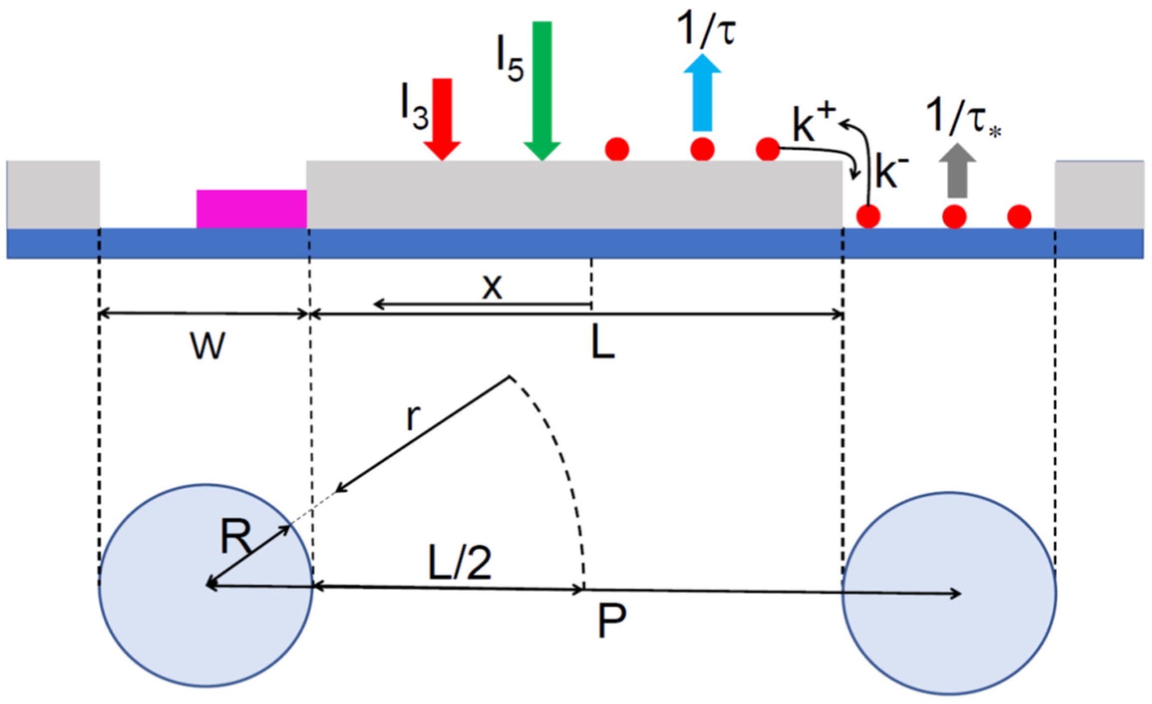
2. Model
2.1. SAG Criterion
2.2. Surface Diffusion of Group III Adatoms
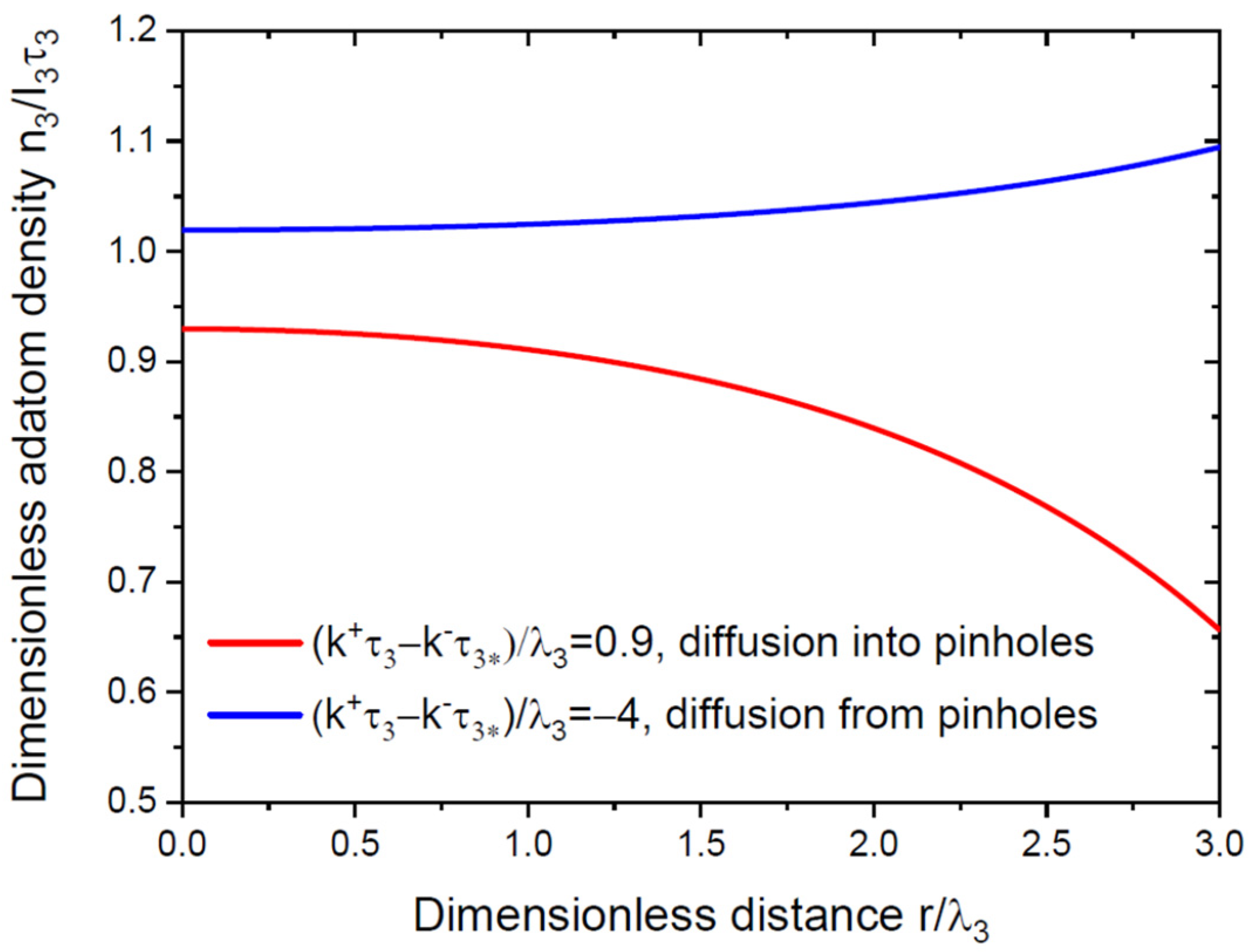
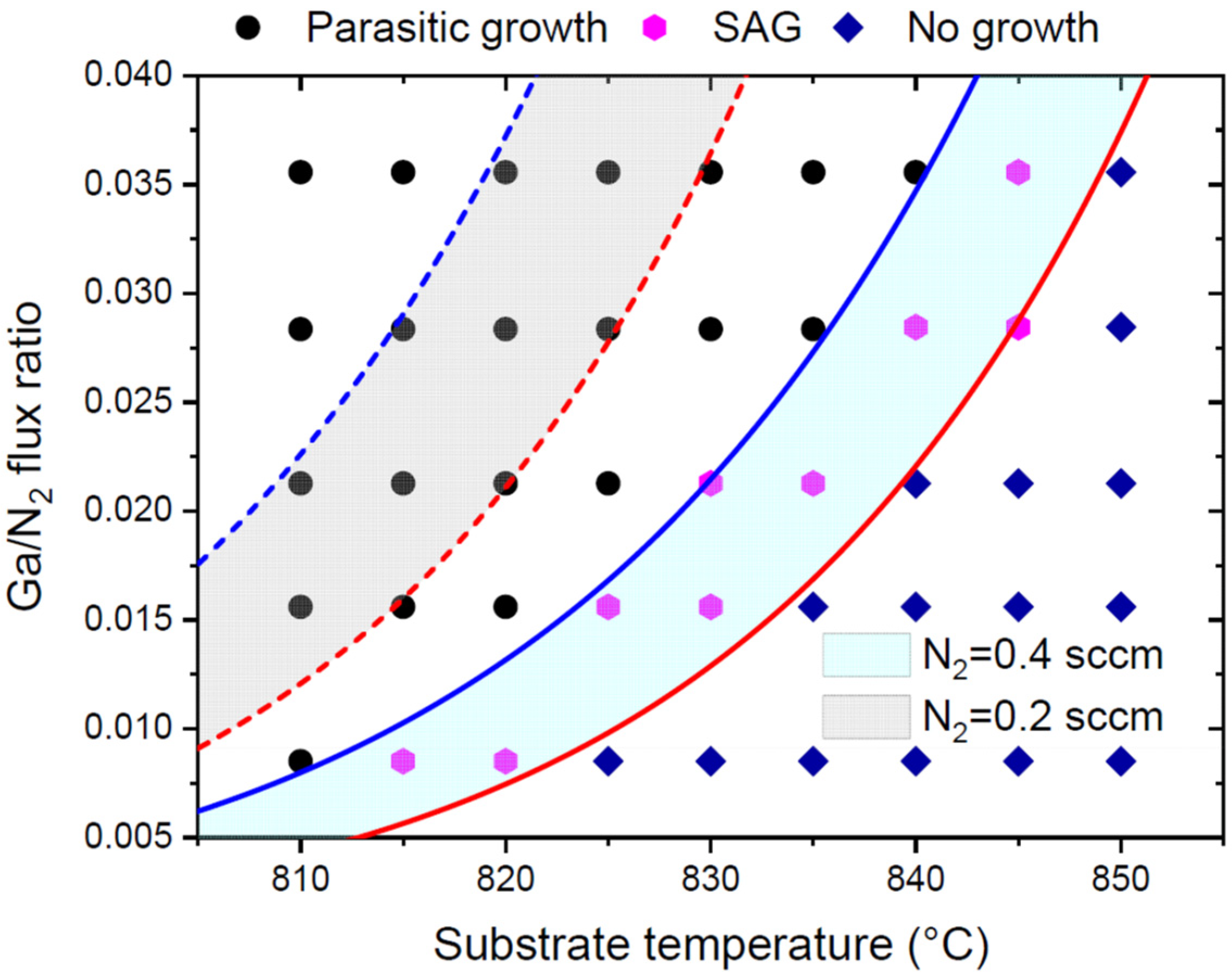
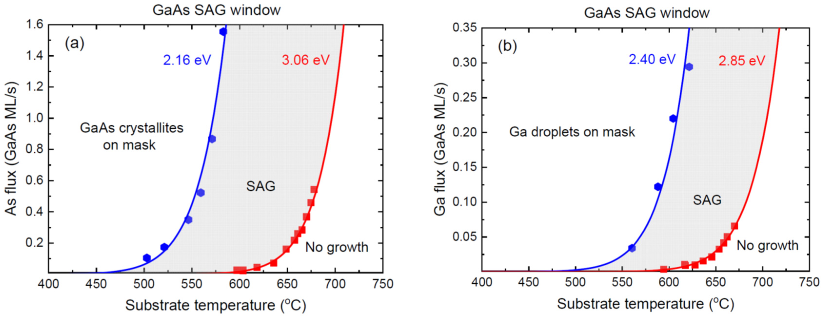
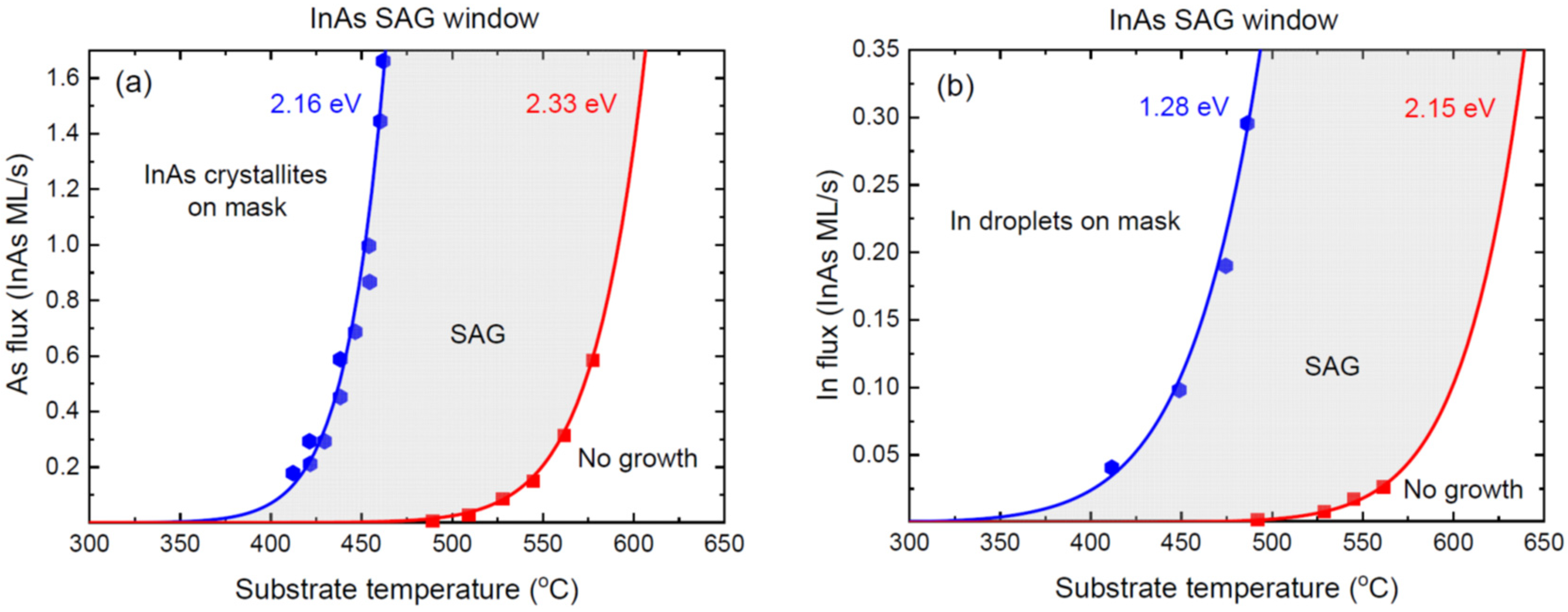
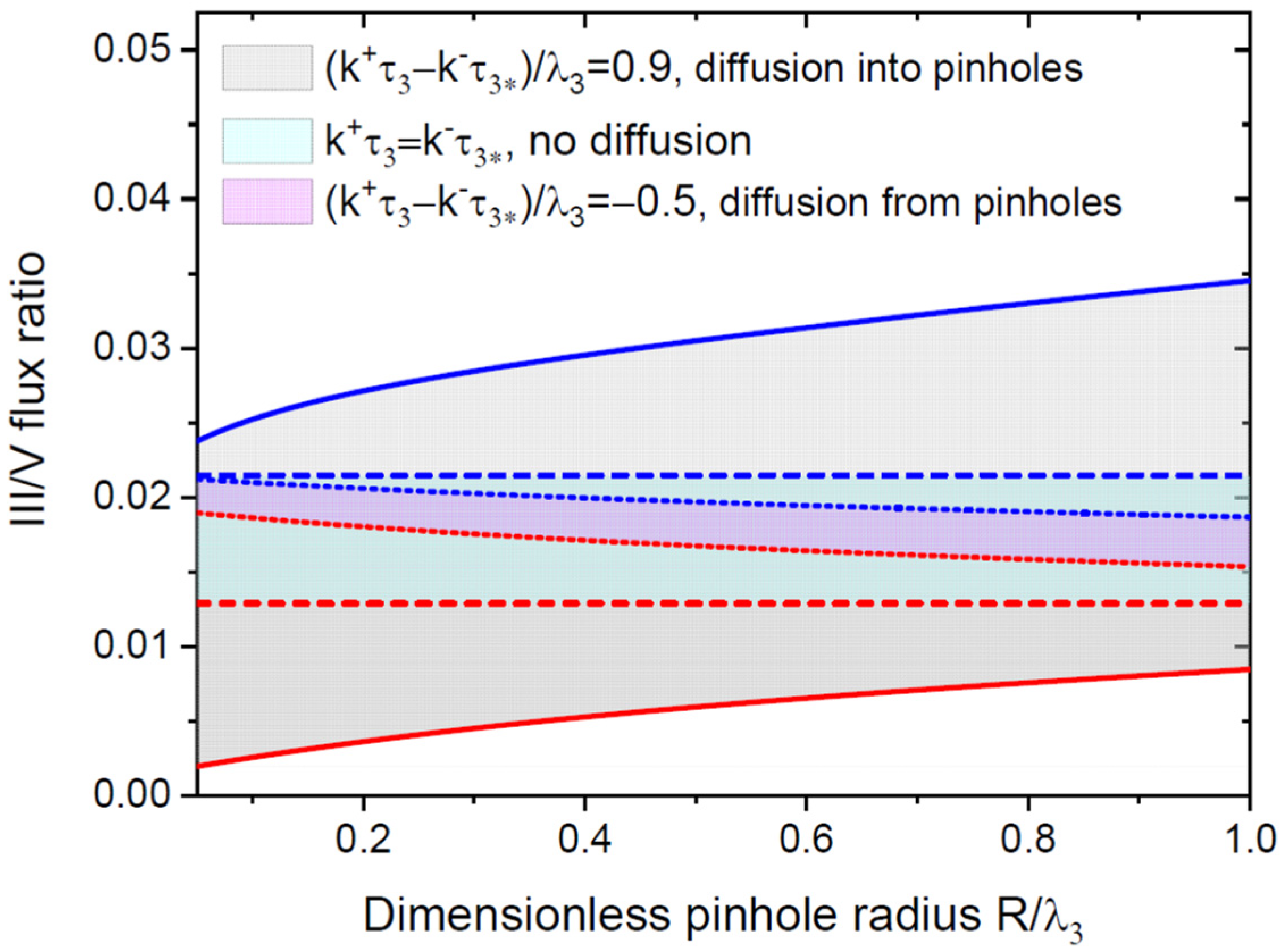
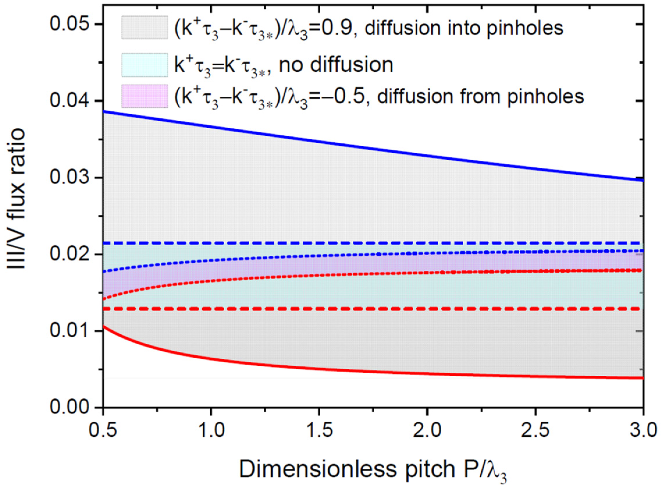
3. Results and Discussion
4. Conclusions
Funding
Data Availability Statement
Conflicts of Interest
References
- Zhang, Y.; Velichko, A.V.; Aruni Fonseka, H.; Parkinson, P.; Gott, J.A.; Davis, G.; Aagesen, M.; Sanchez, A.M.; Mowbray, D.; Liu, H. Defect-free axially stacked GaAs/GaAsP nanowire quantum dots with strong carrier confinement. Nano Lett. 2021, 21, 5722. [Google Scholar] [CrossRef] [PubMed]
- Sekiguchi, H.; Kishino, K.; Kikuchi, A. Emission color control from blue to red with nanocolumn diameter of InGaN/GaN nanocolumn arrays grown on same substrate. Appl. Phys. Lett. 2010, 96, 231104. [Google Scholar] [CrossRef]
- Leandro, L.; Gunnarsson, C.P.; Reznik, R.; Jöns, K.D.; Shtrom, I.; Khrebtov, A.; Kasama, T.; Zwiller, V.; Cirlin, G.; Akopian, N. Nanowire quantum dots tuned to atomic resonances. Nano Lett. 2018, 18, 7217. [Google Scholar] [CrossRef] [Green Version]
- Mauthe, S.; Baumgartner, Y.; Sousa, M.; Ding, Q.; Rossell, M.D.; Schenk, A.; Czornomaz, L.; Moselund, K.E. High-speed III-V nanowire photodetector monolithically integrated on Si. Nat. Commun. 2020, 11, 4565. [Google Scholar] [CrossRef] [PubMed]
- Zhang, H.; Liu, C.-X.; Gazibegovic, S.; Xu, D.; Logan, J.A.; Wang, G.; van Loo, N.; Bommer, J.D.S.; de Moor, M.W.A.; Car, D.; et al. Quantized Majorana conductance. Nature 2018, 556, 74. [Google Scholar] [CrossRef] [PubMed] [Green Version]
- Krogstrup, P.; Ziino, N.L.B.; Chang, W.; Albrecht, S.M.; Madsen, M.H.; Johnson, E.; Nygård, J.; Marcus, C.M.; Jespersen, T.S. Epitaxy of semiconductor–superconductor nanowires. Nat. Mater. 2015, 14, 400. [Google Scholar] [CrossRef] [PubMed]
- Wagner, R.S.; Ellis, W.C. Vapor-liquid-solid mechanism of single crystal growth. Appl. Phys. Lett. 1964, 4, 89. [Google Scholar] [CrossRef]
- Seifert, W.; Borgstrom, M.; Deppert, K.; Dick, K.A.; Johansson, J.; Larsson, M.W.; Martensson, T.; Skold, N.; Svensson, C.P.T.; Wacaser, B.A.; et al. Growth of one-dimensional nanostructures in MOVPE. J. Cryst. Growth 2004, 272, 211. [Google Scholar] [CrossRef]
- Colombo, C.; Spirkoska, D.; Frimmer, M.; Abstreiter, G.; Fontcuberta i Morral, A. Ga-assisted catalyst-free growth mechanism of GaAs nanowires by molecular beam epitaxy. Phys. Rev. B 2008, 77, 155326. [Google Scholar] [CrossRef]
- Oehler, F.; Cattoni, A.; Scaccabarozzi, A.; Patriarche, J.; Glas, F.; Harmand, J.C. Measuring and modeling the growth dynamics of self-catalyzed GaP nanowire arrays. Nano Lett. 2018, 18, 701. [Google Scholar] [CrossRef]
- Noborisaka, J.; Motohisa, J.; Fukui, T. Catalyst-free growth of GaAs nanowires by selective-area metalorganic vapor-phase epitaxy. Appl. Phys. Lett. 2005, 86, 213102. [Google Scholar] [CrossRef] [Green Version]
- Bassett, K.P.; Mohseni, P.K.; Li, X. Evolution of GaAs nanowire geometry in selective area epitaxy. Appl. Phys. Lett. 2015, 106, 133102. [Google Scholar] [CrossRef] [Green Version]
- Tomioka, K.; Ikejiri, K.; Tanaka, T.; Motohisa, J.; Hara, S.; Hiruma, K.; Fukui, T. Selective-area growth of III-V nanowires and their applications. Mater. Res. 2011, 26, 2127. [Google Scholar] [CrossRef]
- Gao, Q.; Dubrovskii, V.G.; Caroff, P.; Wong-Leung, J.; Li, L.; Guo, Y.; Fu, L.; Tan, H.H.; Jagadish, C. Simultaneous selective-area and vapor–liquid–solid growth of InP nanowire arrays. Nano Lett. 2016, 16, 4361. [Google Scholar] [CrossRef] [PubMed]
- Hertenberger, S.; Rudolph, D.; Bichler, M.; Finley, J.J.; Abstreiter, G.; Koblmuüller, G. Growth kinetics in position-controlled and catalyst-free InAs nanowire arrays on Si(111) grown by selective area molecular beam epitaxy. J. Appl. Phys. 2010, 108, 114316. [Google Scholar] [CrossRef] [Green Version]
- Robson, M.T.; Dubrovskii, V.G.; LaPierre, R.R. Conditions for high yield of selective-area epitaxy InAs nanowires on SiOx/Si(111) substrates. Nanotechnology 2015, 26, 465301. [Google Scholar] [CrossRef]
- Kishino, K.; Ishizawa, S. Selective-area growth of GaN nanocolumns on Si (111) substrates for application to nanocolumn emitters with systematic analysis of dislocation filtering effect of nanocolumns. Nanotechnology 2015, 26, 225602. [Google Scholar] [CrossRef]
- Schuster, F.; Hetzl, M.; Weiszer, S.; Garrido, J.A.; De La Mata, M.; Magen, C.; Arbiol, J.; Stutzmann, M. Position-controlled growth of GaN nanowires and nanotubes on diamond by molecular beam epitaxy. Nano Lett. 2015, 15, 1773–1779. [Google Scholar] [CrossRef] [Green Version]
- Kruse, J.; Lymperakis, L.; Eftychis, S.; Adikimenakis, A.; Doundoulakis, G.; Tsagaraki, K.; Androulidaki, M.; Olziersky, A.; Dimitrakis, P.; Ioannou-Sougleridis, V. Selective-area growth of GaN nanowires on SiO2-masked Si (111) substrates by molecular beam epitaxy. J. Appl. Phys. 2016, 119, 224305. [Google Scholar] [CrossRef]
- Gridchin, V.O.; Dvoretckaia, L.N.; Kotlyar, K.P.; Reznik, R.R.; Parfeneva, A.V.; Dragunova, A.S.; Kryzhanovskaya, N.V.; Dubrovskii, V.G.; Cirlin, G.E. Selective area epitaxy of GaN nanowires on Si substrates using microsphere lithography: Experiment and theory. Nanomaterials 2022, 12, 2341. [Google Scholar] [CrossRef]
- Chi, C.-Y.; Chang, C.-C.; Hu, S.; Yeh, T.-W.; Cronin, S.B.; Dapkus, P.D. Twin-free GaAs nanosheets by selective area growth: Implications for defect-free nanostructures. Nano Lett. 2013, 13, 2506. [Google Scholar] [CrossRef] [PubMed]
- Tutuncuoglu, G.; de la Mata, M.; Deiana, D.; Potts, H.; Matteini, F.; Arbiol, J.; Fontcuberta i Morral, A. Towards defect-free 1-D GaAs/AlGaAs heterostructures based on GaAs nanomembranes. Nanoscale 2015, 7, 19453. [Google Scholar] [CrossRef] [PubMed]
- Friedl, M.; Cerveny, K.; Weigele, P.; Tütüncüoglu, G.; Marti-Sanchez, S.; Huang, C.; Patlatiuk, T.; Potts, H.; Sun, Z.; Hill, M.O.; et al. Template-assisted scalable nanowire networks. Nano Lett. 2018, 18, 2666. [Google Scholar] [CrossRef]
- Gooth, J.; Borg, M.; Schmid, H.; Schaller, V.; Wirths, S.; Moselund, K.; Luisier, M.; Karg, S.; Riel, H. Ballistic one-dimensional InAs nanowire cross-junction interconnects. Nano Lett. 2017, 17, 2596. [Google Scholar] [CrossRef]
- Schmid, H.; Borg, M.; Moselund, K.; Gignac, L.; Breslin, C.M.; Bruley, J.; Cutaia, D.; Riel, H. Template-assisted selective epitaxy of III–V nanoscale devices for co-planar heterogeneous integration with Si. Appl. Phys. Lett. 2015, 106, 233101. [Google Scholar] [CrossRef]
- Aseev, P.; Fursina, A.; Boekhout, F.; Krizek, F.; Sestoft, J.E.; Borsoi, F.; Heedt, S.; Wang, G.; Binci, L.; Martí-Sánchez, S.; et al. Selectivity map for molecular beam epitaxy of advanced III-V quantum nanowire networks. Nano Lett. 2019, 19, 218. [Google Scholar] [CrossRef] [PubMed]
- Yuan, X.; Pan, D.; Zhou, Y.; Zhang, X.; Peng, K.; Zhao, B.; Deng, M.; He, J.; Tan, H.H.; Jagadish, C. Selective area epitaxy of III–V nanostructure arrays and networks: Growth, applications, and future directions. Appl. Phys. Reviews 2021, 8, 021302. [Google Scholar] [CrossRef]
- Okamoto, A.; Ohata, K. Selective epitaxial growth of gallium arsenide by molecular beam epitaxy. Appl. Phys. Lett. 1987, 51, 1512. [Google Scholar] [CrossRef]
- Okamoto, A.; Ohata, K. Selective epitaxial growth of InAs on GaAs by molecular beam epitaxy. Jpn. J. Appl. Phys. 1987, 26, L1174. [Google Scholar] [CrossRef]
- Allegretti, F.; Inoue, M.; Nishinaga, T. In-situ observation of GaAs selective epitaxy on GaAs (111)B substrates. J. Cryst. Growth 1995, 146, 354. [Google Scholar] [CrossRef]
- Dubrovskii, V.G. Gallium diffusion flow direction during deposition on the surface with regular hole arrays. Tech. Phys. Lett. 2021, 47, 601. [Google Scholar] [CrossRef]
- Dede, D.; Glas, F.; Piazza, V.; Morgan, N.; Friedl, M.; Guniat, L.; Nur Dayi, E.; Balgarkashi, A.; Dubrovski, V.G.; Fontcuberta i Morral, A. Selective area epitaxy of GaAs: The unintuitive role of feature size and pitch. Nanotechnology 2022, 33, 485604. [Google Scholar] [CrossRef] [PubMed]
- Dubrovskii, V.G. Nucleation Theory and Growth of Nanostructures; Springer: Cham, Switzerland, 2014. [Google Scholar]
- Kelrich, A.; Dubrovskii, V.G.; Calahorra, Y.; Cohen, S.; Ritter, D. Control of morphology and crystal purity of InP nanowires by variation of phosphine flux during selective area MOMBE. Nanotechnology 2015, 26, 085303. [Google Scholar] [CrossRef] [PubMed]
- Kukushkin, S.A.; Osipov, A.V. New phase formation on solid surfaces and thin film condensation. Prog. Surf. Sci. 1996, 51, 1. [Google Scholar] [CrossRef]
- Hanggi, P.; Talkner, P.; Borkovec, M. Reaction-rate theory: Fifty years after Kramers. Rev. Mod. Phys. 1990, 62, 251. [Google Scholar] [CrossRef]
- Dubrovskii, V.G.; Hervieu, Y.Y. Diffusion-induced growth of nanowires: Generalized boundary conditions and self-consistent kinetic equation. J. Cryst. Growth 2014, 401, 431. [Google Scholar] [CrossRef]
- Schwoebel, R.L. Step motion on crystal surfaces. J. Appl. Phys. 1966, 37, 3682. [Google Scholar] [CrossRef]
Publisher’s Note: MDPI stays neutral with regard to jurisdictional claims in published maps and institutional affiliations. |
© 2022 by the author. Licensee MDPI, Basel, Switzerland. This article is an open access article distributed under the terms and conditions of the Creative Commons Attribution (CC BY) license (https://creativecommons.org/licenses/by/4.0/).
Share and Cite
Dubrovskii, V.G. Criterion for Selective Area Growth of III-V Nanowires. Nanomaterials 2022, 12, 3698. https://doi.org/10.3390/nano12203698
Dubrovskii VG. Criterion for Selective Area Growth of III-V Nanowires. Nanomaterials. 2022; 12(20):3698. https://doi.org/10.3390/nano12203698
Chicago/Turabian StyleDubrovskii, Vladimir G. 2022. "Criterion for Selective Area Growth of III-V Nanowires" Nanomaterials 12, no. 20: 3698. https://doi.org/10.3390/nano12203698
APA StyleDubrovskii, V. G. (2022). Criterion for Selective Area Growth of III-V Nanowires. Nanomaterials, 12(20), 3698. https://doi.org/10.3390/nano12203698