Abstract
Herein, we reported a unique photo device consisting of monolayer graphene and a few-layer rhenium diselenide (ReSe2) heterojunction. The prepared Gr/ReSe2-HS demonstrated an excellent mobility of 380 cm2/Vs, current on/off ratio ~ 104, photoresponsivity (R ~ 74 AW−1 @ 82 mW cm−2), detectivity (D* ~ 1.25 × 10¹¹ Jones), external quantum efficiency (EQE ~ 173%) and rapid photoresponse (rise/fall time ~ 75/3 µs) significantly higher to an individual ReSe2 device (mobility = 36 cm2 V−1s−1, Ion/Ioff ratio = 1.4 × 10⁵–1.8 × 10⁵, R = 11.2 AW−1, D* = 1.02 × 10¹⁰, EQE ~ 26.1%, rise/fall time = 2.37/5.03 s). Additionally, gate-bias dependent Schottky barrier height (SBH) estimation for individual ReSe2 (45 meV at Vbg = 40 V) and Gr/ReSe2-HS (9.02 meV at Vbg = 40 V) revealed a low value for the heterostructure, confirming dry transfer technique to be successful in fabricating an interfacial defects-free junction. In addition, HS is fully capable to demonstrate an excellent gas sensing response with rapid response/recovery time (39/126 s for NO2 at 200 ppb) and is operational at room temperature (26.85 °C). The proposed Gr/ReSe2-HS is capable of demonstrating excellent electro-optical, as well as gas sensing, performance simultaneously and, therefore, can be used as a building block to fabricate next-generation photodetectors and gas sensors.
1. Introduction
Graphene and other two-dimensional (2D) materials, particularly transition metal dichalcogenides (TMDs), have attracted much attention due to their unique electro-optical properties [1,2,3]. TMDs consist of smooth surfaces without any dangling bonds and possess significantly low surface states and trapping defects that cumulatively enable rapid charge speed and suppress charge scattering even in a few nanometer-thick layers [4]. Using these materials, the scientific community is able to develop many proof-of-concept devices such as field effect transistors (FETs) [5,6,7], photodetectors [8,9,10], supercapacitors [5,11], solar cells [12], gas sensors [13], electrochemical sensors [14] and biosensors [15,16,17], etc., for years. Amongst these, photodetectors and gas sensors are of significant interest as these possess the capacity of resolving energy and environmental concerns to a certain level [18]. Interestingly, in contrast to graphene (a zero bandgap material) [19], TMDs have finite bandgap values normally between 0.2 to 3 eV [20] depending upon the choice of material and its layer thickness and were found to be a potential substitute for traditional narrow bandgap materials for many electronic and optoelectronic applications. Moreover, their properties are strongly influenced by the choice of metal contacts (either ohmic or Schottky), energy band alignment, and types of TMDs [21]. Additionally, their electro-optical and gas sensor characteristics can also be modified by the electrostatic backgate voltage as well as channel region doping [22,23].
Furthermore, heterostructures (HS) fabricated on either TMDs or with other low-dimensional electronic materials have been found to demonstrate outstanding optoelectronic and gas sensing performance in comparison to their counterparts [24,25,26]. For instance, PbS quantum dots (PbS-QDs)/MoS2 heterostructure have shown a tremendously high photoresponsivity (~6 × 10⁵ AW−1) as compared to only an MoS2 photodetector. Such remarkable photoresponse properties are associated with strong light absorption characteristics of PbS-QDs [27]. Previously, we have demonstrated ZnO-QDs drop cast over MoS2 nanosheets to study their electro-optical characteristics. The calculated photoresponsivity was found to be 2 × 10³ AW−1 [28]. Despite excellent photoresponse, these photodetectors have demonstrated low response speeds (0.1–10 s). This limited performance is ascribed to low response rates as well as the environmental hazard nature (Zn or Pb leaching) of QDs [29]. For the development of next-generation optoelectronic devices, high responsivity and rapid photoresponse is a prerequisite. To circumvent this issue, HS based on graphene and 2D TMDs have been established to improve photoresponse speed as well as photoresponsivity. For instance, the graphene/WS2 photodetector exhibited a responsivity of ~950 AW−1 with a response time of 7.85 s [30]. In another study, graphene/MoTe2 demonstrated a responsivity of ~971 AW−1 with a response time of 78 msec [31]. Such reasonable response speed is attributed to graphene’s high carrier transport [32].
Moving onward, 2D-materials-based gas sensors have also been found to be of significant interest. From the literature, the gas sensing response strictly depends upon the surface-to-volume ratio (SVR) of the material [33]. In this perspective, graphene was believed to outperform conventional sensors as its atomically thin layered structure possesses ultimately high SVR [34]. However, in addition to SVR, other factors that can influence gas sensing response are semiconducting properties and the density of available reactive sites for the occurrence of redox reactions [35,36]. Since individual graphene layers have no bandgap, however, stacking graphene to other TMDs can resolve this problem as the semiconducting properties of TMDs can easily be modified by the electrostatic gate bias or exposure to light and therefore, gas sensing response can be modulated/improved. Several 2D materials such as MoS2, GaSe, GaS, hBN, WSe2, etc. were investigated for gas sensing however, there is not much literature available on graphene-based TMDs heterostructures used as gas sensors [13].
Among various TMDs out there, rhenium diselenide (ReSe2) has been found as an excellent 2D semiconducting material possessing a theoretically measured DFT-based direct narrow bandgap (~0.995 (bulk)–1.239 eV (monolayer)) [37] which is significantly lower than conventional TMDs [38]. Recently, Kim et al. [23] investigated HCl-mediated p-doping of ReSe2 and reported an improved photoresponsivity of 1.93 × 10³ AW−1 and photoresponse rise/decay time of 1.4/3.1 ms as compared to undoped ReSe2 (photoresponsivity = 79.99 AW−1, rise/decay time = 10.5 ms/291 ms). Bach et al. [39] have studied Gr/ReSe2 barristor devices, however, with limited photoresponsivity of 42 AW−1 and rise/decay time of 33.9/20.8 ms under a high laser wavelength of 656 nm with a light intensity of 189 mW/cm2. However, these reports demonstrated lower photoresponse time. Moreover, no gas-sensing performance was demonstrated in these devices. Therefore, it is of great interest to develop a heterostructure that can demonstrate good electro-optical and gas sensing characteristics simultaneously within a single device.
Herein, we have successfully developed a Gr/ReSe2 hybrid device that can demonstrate exceptional photodetector and gas sensing performance, simultaneously. In our device, graphene and ReSe2 flakes work as transport and light absorption layers, respectively. We have drawn a comparative analysis of electro-optical performance between individual ReSe2 and Gr/ReSe2 devices. The results indicate that the Gr/ReSe2 photodetector has considerable photoresponsivity (R ~ 74 AW−1 at 82 mW cm−2), detectivity (D* ~ 1.25 × 10¹¹ Jones) and a high photoresponse (rise/decay ~ 75/3 μs) as compared to an individual ReSe2 device (R = 11.2 AW−1, D* = 1.02 × 10¹⁰, rise/fall time = 2.37/5.03 s). Moreover, the photocurrent and photoresponsivity were calculated as a function of laser light intensity. Furthermore, Schottky barrier height (SBH) evaluation has revealed Gr/ReSe2 devices demonstrating low SBH (9.02 meV at Vbg = 40 V) which is the reason behind the high electro-optical performance of the HS. Finally, Gr/ReSe2-HS was tested for NO2 gas sensing (20–200 ppb). The exceptional performance of our devices is ascribed to high-quality graphene, a suitable choice of ReSe2 flake, residual-free PDMS stamp supported transfer technique and choice of metal electrodes that eventually reveal low SBH.
2. Experimental Detail
2.1. Device Fabrication
Here, a vertical heterostructure (HS) composed of mono-layer graphene and few-layer ReSe2 was prepared over SiO2 (300 nm)/p+-Si substrate. Figure S1 illustrates step-by-step fabrication detail about HS formation. Briefly, CVD-grown monolayer graphene was transferred over SiO2/Si substrate by employing the wet transfer method reported elsewhere [40]. As-transferred graphene layer was then patterned into a rectangular shape (hall bar) using photolithography and an oxygen plasma etching process. During O2 etching, graphene was treated by power (~50 W) for a few minutes to etch undesired graphene. To make a large pattern around the graphene hall bar, a second photolithography process was carried out after which the defined electrodes were filled by Cr/Au (5/30 nm) deposition. On completion of the deposition, the devices were left in acetone for several hours to accomplish the lift-off process.
On another substrate (SiO2 (300 nm)/p+-Si), we used the scotch-tape method to mechanically exfoliate the ReSe2 flake. An optical microscope was used to find a suitable ReSe2 flake of a few-layers thickness which was later transferred to a pre-patterned graphene hall bar using a PDMS stamp and micromanipulator. In the end, the e-beam lithography process followed by Cr/Au (8/120 nm) deposition and subsequent lift-off in acetone were conducted to make final electrical connections to Gr/ReSe2 HS. Additionally, a moderate temperature annealing process (200 °C for 4 h) was also carried out in a tube furnace under Ar/H2 (97.5%/2.5%) gas flow to improve adhesion between metal electrodes and flake surfaces.
2.2. Characterization
Raman analysis was examined using micro-Raman (Renishaw, Wotton-under-Edge, UK) for monolayer graphene, few-layer ReSe2, and Gr/ReSe2 HS. A laser wavelength (514 nm) of low-power intensity (511 μW) with a spot size of 0.7 μm was used to avoid any kind of structural deterioration due to the laser heating effect. Furthermore, to realize the exact thickness of graphene and ReSe2 flakes, atomic force microscopy (AFM; n-Tracer, NanoFocus, Oberhausen, Germany) in tapping mode was used.
2.3. Electrical and Electro-Optical Measurement
For electrical measurement, Keithley 2400 and Keithley 6485 K (Keithley Instruments, Inc., Cleveland, OH, USA) were used as source meter and picoammeter, respectively. The complete electrical measurement was performed at room temperature and under vacuum (10−3 Torr) conditions. Further, to estimate Schottky barrier height (SBH), the device’s electrical measurement was achieved in the low-temperature range (30–300 K) under high vacuum (10−4 to 10−5 Torr). Moreover, to study electro-optical measurement, the devices were tested using the same systems (Keithley 2400 and Keithley 6485 K) under a vacuum in the dark and under laser light irradiation (532 nm) of varying power intensity (82–820 mW cm−2).
2.4. NO2 Gas Sensing Measurement
To further test the Gr/ReSe2 heterostructure ability to sense NO2 gas, an experimental setup illustrated in Figure S5 was utilized. The desired concentration was achieved by mixing NO2 (2%) and N2 (98%) before injecting them into the chamber. For this purpose, a mass flow controller (MFC) was employed which can control concentration and maintain a total gas flow rate of around 1000 sccm throughout the experiment. The gas is injected inside the chamber in such a manner that it reaches the Gr/ReSe2 HS-based sensor device within a few seconds. Such an experimental arrangement is very effective as it can detect any environmental change quickly. All the measurement was conducted at room temperature (26.85 °C) under ambient atmospheric conditions. The device was also irradiated with light illumination of 532 nm with a power intensity of 310 mW cm−2 to enhance the gas sensing response of the heterostructure.
3. Results and Discussion
Figure 1a,b illustrates a schematic diagram and an actual device optical image of graphene/ReSe2 van der Waals heterostructure, respectively, fabricated at Si/SiO2 substrate and after Cr/Au contacts deposition via e-beam lithography process (scale bar: 5 µm). Figure S1 represents the device fabrication detail and the various steps involved. In brief, CVD-grown monolayer graphene was first etched into a rectangular bar after which a pristine ReSe2 flake of appropriate thickness was exfoliated over polydimethylsiloxane (PDMS) stamp, was transferred onto graphene and interacted through van der Waals forces using micromanipulation process. Of note, the photodetector devices based on individual ReSe2 and graphene/ReSe2 heterostructures have used the same ReSe2 flake to avoid any discrepancy while measuring photodetector device performance, as different ReSe2 flakes could have a different capacity for demonstrating photoresponse.
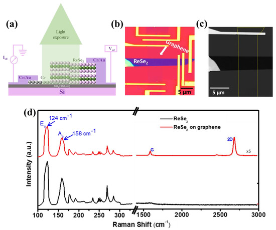
Figure 1.
(a) Schematic illustration and (b) real device optical image of graphene/ReSe2 van der Waals heterostructure (scale bar; 5 µm), (c) SEM micrograph (scale bar; 5 µm), whereas yellow dotted line indicate graphene layer. (d) Raman analysis of ReSe2 (black curve) and graphene/ReSe2 heterostructure (red curve).
Further, Figure 1c represents a scanning electron microscope (SEM) micrograph (scale bar: 5 µm) which reveals a clear heterostructure without any deformation or contamination during the transfer process (yellow dotted line indicates the boundary of monolayer graphene). To further visualize the uniformity of the material and to evaluate the accurate thickness of the ReSe2 flake, the atomic force microscopy (AFM) image and corresponding height profile are presented in Figure S2. The AFM scanning reveals ReSe2 thickness to be around ~6.4 nm, approximately nine layers [41].
Raman analysis of ReSe2 and graphene/ReSe2 heterostructure have revealed several distinct peaks between the ranges 100–300 cm−1, ascribed to the interlayer vibrational decoupling in ReSe2 (Figure 1d). The prominent peaks related to ReSe2 were observed at 124 and 158 cm−1. These are associated with in-plane (Eg) and out-of-plane (Ag) vibrational modes, respectively [42]. Furthermore, in the case of graphene/ReSe2 heterostructure, some additional peaks related to monolayer graphene were observed; G-peak positioned at 1580 cm−1 and is related to in-plane phonon mode, and 2D-peak located at ~2700 cm−1 is ascribed to double resonance [39,43].
3.1. ReSe2 Device Electrical Performance
To explore the device’s performance and to investigate the advantage of graphene in the heterostructure, the device’s electrical properties were realized from both pristine ReSe2 channel and Gr/ReSe2 heterostructure. Figure 2 illustrates the electrical performance of a few-layer ReSe2 flake fabricated on a Si/SiO2 substrate. The transfer characteristics (Ids–Vbg) were studied at Vds = 0.2–1 V and are presented both in linear-, and log-scale as shown in Figure 2a,b, respectively. A bias-dependent increase in on-current (Ion) has been observed on increasing Vds from 0.2 to 1 V which demonstrates usual ReSe2 transistor characteristics, similar to work [22,44]. The field-effect mobility denoted as µFE can be evaluated by the following relation:
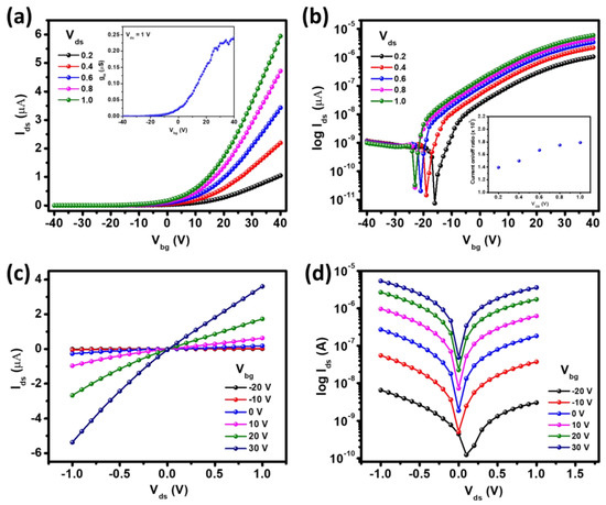
Figure 2.
Transfer characteristics (Ids-Vbg) of ReSe2 at Vds = 0.2–1.0 V (a) in linear scale, and (b) in log scale (inset: current on/off ratio measured at Vds = 0.2–1.0 V)). Output characteristics (Ids–Vds) in Vbg range from −20 to 30 V (c) in linear scale, and (d) in log scale.
In the above relation, the letters “L” and “W” indicate the length and width of the ReSe2 channel, denotes slope related to transfer characteristics, and (115 aF/μm2) represents gate capacitance [45,46,47]. The calculated mobility for the ReSe2 transistor was 36 cm2/Vs. In addition, the Vbg-dependent trend of transconductance (gm(µS) = ) of ReSe2-based FET was presented (inset: Figure 2a) which demonstrate that the proposed devices possess promising potential of delivering larger gain. Furthermore, to find the suitability of the prepared ReSe2 transistors for digital applications, the devices must possess a current on/off ratio (Ion/Ioff) of at least 104 [48]. Figure 2b presents log-scale Ids–Vbg characteristics and the corresponding calculated Ion/Ioff ratio as the inset. Interestingly, the calculated Ion/Ioff ratio (~1.4 × 10⁵–1.8 × 10⁵) demonstrates an increasing trend with Vds possibly due to an increase in on-current as observed in Ids–Vbg characteristics. The calculated mobility and Ion/Ioff are reasonably higher than the minimum requirement and surpass most of the previously reported TMDs on the Si/SiO2 substrate. Moving further, the output characteristics (Ids–Vds) related to the ReSe2 transistor were evaluated, as presented in linear scale (Figure 2c) and log-scale (Figure 2d), respectively. Almost linear Ids–Vds characteristics in the low bias (±Vds) region reveal that the Cr/Au contact established nearly ohmic contact with the ReSe2 channel with low Schottky barrier height (see Section 3.3), as observed previously [49].
After the electrical transport measurement of the ReSe2 transistor, a detailed transport measurement was carried out to evaluate Gr/ReSe2 heterostructure electro-optical performance. Figure 3a illustrates the transfer characteristics (Ids–Vbg) of Gr/ReSe2 van der Waals heterostructure both in linear-, and log-scale at Vds = 1 V. It is noteworthy that the heterostructure demonstrates similar transfer characteristics as of pristine ReSe2 transistor (Figure 2a); however, a high on-current was observed in the heterostructure as compared to pristine ReSe2. This is ascribed to the higher carrier mobility of graphene [24]. The detailed transport characteristics (transfer and output) of pristine graphene are also presented in Figure S3. A charge-neutral point (CNP) also known as a Dirac point (DP) was observed around −8 V at Vds = 0.1 V (Figure S3a), which indicates the graphene is a kind of n-doped graphene [50]. It should be noted here that no intentional doping was performed during the synthesis or transfer process. Therefore, the present monolayer graphene is regarded as pristine graphene. Further, the mobility was calculated using the relation μ = (1/Cbg) (∂σ/∂Vbg), where σ = 1/ρ represents sample conductivity. The measured value of electron mobility for monolayer graphene was around 1350 cm2/Vs. In addition, the output characteristics (Ids–Vds) were also performed (Figure S3b) which shows a linear relation, revealing the ohmic nature of Cr/Au contact with monolayer graphene. Such remarkable performance of monolayer graphene is the key reason for the high-performing Gr/ReSe2 heterostructure where we have observed mobility of 380 cm2/Vs and an on/off ratio ~ 104). Here, Gr/ReSe2 heterostructure was prepared using CVD-grown monolayer graphene over which an exfoliated ReSe2 flake was transferred. Such heterostructure was also reported previously, however with a limited Ion/Ioff ratio of ~102 [39]. However, the present work has demonstrated an Ion/Ioff ratio (104), revealing the potential of the studied heterostructure for switching applications. The limited Ion/Ioff could be ascribed to graphene’s semi-metallic nature where the Fermi level of graphene and the related work function varies with bias voltage, resulting in controlled carrier transportation across valence/conduction bands. Moreover, the defects during the growth process of graphene and impurities through the transfer process could also play a significant role in controlling device electro-optical performance [51].
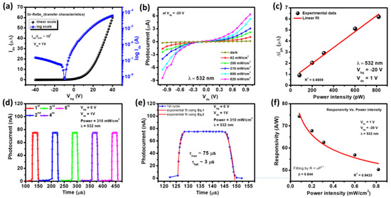
Figure 3.
Graphene/ReSe2 heterostructure characteristics: (a) transfer characteristics (Ids–Vbg) both in linear (black curve) and log-scale (blue curve) measured at Vds = 1 V showing on/off ratio of ~104. (b) Output characteristics (Ids–Vds) in dark and under various light intensities (82–820 mW/cm2) conditions measured at Vbg = −20 V and incident light wavelength of 532 nm. (c) Observation of linear relationship between ΔIph = Iph – Idark and light power intensities evaluated at Vbg = −20 V, Vds = 1 V, and λ = 532 nm (where R2 = 0.9859). (d) Measurement of photocurrent for five consecutive cycles without any biasing at Vds = 1V, power = 310 mW/cm2, and λ = 532 nm. (e) Corresponding measurement of photoresponse (rise time (75 µs) and fall time (3 µs)) of the graphene/ReSe2 heterostructure-based photodetector. (f) Responsivity versus power intensity trend follows relationship R = αPβ−1 with calculated β = 0.844.
3.2. Gr/ReSe2 Photodetector Response
To evaluate the photodetector performance based on Gr/ReSe2 heterostructure, photocurrent measurement as a function of Vds at a fixed Vbg = −20 V and λ = 532 nm was presented in Figure 3b. The measured photocurrent at various incident light intensities is significantly higher than what has been observed under dark conditions, revealing the excellent photoresponse of active charge carriers inside the Gr/ReSe2 heterostructure. Interestingly, a linear relationship between ΔIph and light power intensities has been observed (Figure 3c) which indicates that the larger the light intensity, the higher will be the electron-hole pair generation which leads to the generation of high photocurrent in these devices [52]. Further, a cyclic measurement was performed which measured photocurrent for five consecutive cycles without any bias voltage at a power intensity of 310 mW/cm2, Vds = 1 V and λ = 532 nm (Figure 3d). In this way, Gr/ReSe2 heterostructure photoresponse stability and results repeatability was verified. Noteworthy, the devices were measured under vacuum conditions to avoid external oxygen or water molecules device degradation. Moreover, the photoresponse was estimated at Vbg = 0 V to remove gate dependency or current contribution. However, the supplied Vds was maintained at 1 V to facilitate drift to charge carriers in the channel region of the Gr/ReSe2 heterostructure. Furthermore, the photoresponse, i.e., the rise and fall time of the photodetector as a function of time, was estimated as shown in Figure 3e. The rise time (τrise) and fall time (τfall) of the photodetector was calculated using the following fitting equations [28]:
where “Iph(t)” represents time-dependent photocurrent, “Idark” indicate dark current under no light illumination, “t” denotes light switching time, and “A” is equation constant. Equations (2) and (3) were used to estimate the rise and fall time of the Gr/ReSe2-based photodetector. The calculated values for rise/fall time were 75/3 µs, significantly higher than most of the studied TMDs-based photodetectors [53,54,55]. We have also evaluated photoresponse characteristics from only the ReSe2 channel-based photodetector (Figure S4). The results indicate that Gr/ReSe2 photodetector has higher photo characteristics as compared to the ReSe2-based photodetector. In addition to the response time, several other important photodetector performance parameters such as photoresponsivity (Rλ), external quantum efficiency (EQE%), and detectivity (D*) were evaluated and are presented in Figure 3f and Figure 4, respectively. The “Rλ” is equal to photocurrent produced as a unit of light intensity incident on the effective channel area of the photodetector and is given by the relation [56]:
where = is the produced photocurrent, “P” denotes light intensity (82–310 mW/cm2) and “A” represents the device-effective area. The calculated Rλ as a function of power intensity is presented in Figure 3f and has values between (50–75 A/W). Responsivity decreases as laser power increases. This trend was fitted by the equation where and β are constants whereas P corresponds to optical power. The calculated value of β was around 0.844 at maximum fit with R2 = 0.9423. The calculated value of for Gr/ReSe2 photodetector is almost 7 times higher than ReSe2 photodetector (Responsivity ~11.2 AW−1).
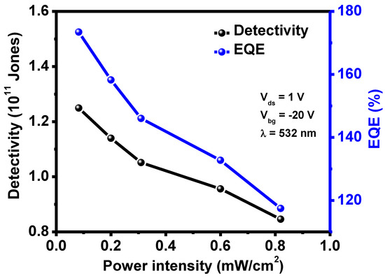
Figure 4.
Calculation of detectivity (D*) and external quantum efficiency (EQE%) measured at Vds = 1V, Vbg = −20 V, and λ = 532 nm.
EQE is the number of charge carriers produced per incident photon and mathematically expressed as [22]:
where, h, c, and λ are plank’s constant, speed of light and wavelength of the incident light, respectively. Interestingly, the EQE value is highly dependent on incident light wavelength, and for a fixed value of wavelength, it depends upon the value of photoresponsivity as other factors are constant. Figure 4 demonstrates a decreasing trend of EQE as a function of laser intensity and follows a similar trend as responsivity. The estimated EQE value was between 117–173% higher than the ReSe2 photodetector (EQE ~ 26.1%).
Detectivity (D*) is defined as the device’s ability to detect signals of a weaker strength. This is mathematically given by the relation [28,57]:
D* is described in the unit of Jones, and one Jones = 1 cm Hz1/2 W−1 and Idark represent current under no illumination. Figure 4 shows D* as a function of light intensity follows a decreasing trend just like responsivity and EQE. It has values between 0.8–1.2 × 10¹¹, significantly higher than ReSe2 photodetector (D* ~ 1.02 × 10¹⁰ Jones). All these results indicate Gr/ReSe2 van der Waals heterostructure-based photodetector has superior performance compared to only the ReSe2 material-based photodetector. This means graphene has a governing role in outperforming Gr/ReSe2 photodetector as it enhances transport rates of photo-carriers produced in ReSe2 due to the high carrier mobility provided by graphene. The photodetector performance was compared to previously published reports as presented in Table 1.
3.3. SBH Estimation
Next, we have estimated Schottky barrier height (SBH) denoted as ΦSBH, and describe it as an energy barrier faced by the electrons while moving across the metal-semiconductor junction. Schottky–Mott’s rule was used to predict the value of ΦSBH. It states that the ΦSBH varies proportionally with the difference between the semiconductor’s electron affinity and the metal’s work function. Interestingly, many semiconductors do not satisfy this rule due to the generation of metal-induced gap states which pin the bandgap close to the Fermi level. Such unwanted effect is regarded as Fermi-level pinning [58]. Therefore, it is highly desirable to select proper metal and semiconductors to minimize SBH value so that devices with ultimate electro-optical performance could be achieved. Here we chose Cr metal (work function ~ 4.5 eV) [59] to deposit as electrodes over the semiconductor (i.e., ReSe2 devices) and Gr/ReSe2 heterostructure to define the channel. Temperature-dependent transfer characteristics (Ids-Vbg) for the ReSe2 transistor and Gr/ReSe2 heterostructure were determined and presented in Figure 5a,b. The curves were obtained at various temperatures (300, 250, 200, 180, 140, 120, 100, 80, 50 and 30 K). Noteworthy, in the transfer curve, the current values increase as the temperature increases contrary to previous reports which claim a kind of metal-to-insulator transition (MIT) around 200 K [22]. Since the devices prepared in the present work are realized over Si/SiO2 substrate, which possesses several impurities or defect states, it therefore hinders MIT observation in these devices. From the literature, it has been studied that gate-dependent carrier transport in thin layers of TMDs located near to dielectric substrate is strongly affected by the impurities and various disorders from the dielectric substrate. Therefore, these devices do not demonstrate MIT, which is in agreement with what we have observed in the present study. Moving further, the SBH value was calculated considering standard thermionic emission theory and using the below relationship [60]:
where represents the device’s effective area, A* is Richardson’s constant, source-drain current through the device channel, Vds indicate source-drain voltage, is the ideality factor, q represents electron charge, T is temperature and is the Boltzmann constants.
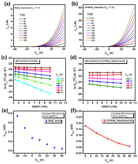
Figure 5.
(a) Temperature-dependent transfer curves (Ids–Vg) of ReSe2 and (b) Gr/ReSe2 transistors for temperature range 30–300 K and Vds = 1V. No MIT evidence is visible. Richardson plot between ln (Ids/T2) and 1000/T at various Vbg for (c) ReSe2 device, and (d) Gr/ReSe2 heterostructure device. (e) Extracted SBH values versus Vbg for the ReSe2 device. (f) Extracted SBH values versus Vbg for Gr/ReSe2 device.
Figure 5c,d illustrates individual ReSe2 and Gr/ReSe2 heterostructure device’s Richardson plot, i.e., ln (Is/T2) versus q/T in the reverse bias saturation regime where the obtained data was linearly fitted for each Vbg value. Based on the concept of thermionic emission theory, the slope of linearly fitted curves gives the value of Schottky barrier height (ΦSBH) as presented in Figure 5e,f. Interestingly, the calculated values of ΦSBH are lower/higher at positive/negative Vbg values and do not vary linearly with the gate voltage. Moreover, there could exist three different transport regimes based on applied Vbg [61]. At low Vbg, the device was considered in a switch-off state with the highest value of ΦSBH and the only transport existed due to the thermal agitation of electrons crossing the barrier. Upon increasing Vbg, the ΦSBH decreases and the conduction band of ReSe2 started moving downward resulting in an exponential rise of current as obvious from the transfer characteristics of Figure 2b. Upon further increase in Vbg, a flat band condition (Vbg = VFB) reaches which exists in the subthreshold region of transfer characteristics. Moving on, for Vbg > VFB, the device underwent a Schottky band regime as obvious by the bent downward part of Ids–Vbg characteristics, revealing a combination of thermionic and field emission transport. Finally, with more increase in Vbg, there exist a tunneling current through Cr/ReSe2 barrier which became the major transport mechanism leading to the linear region in Ids–Vbg characteristics. As the devices are prepared over Si/SiO2 substrates, therefore, a lot of charge impurities and surface traps are expected from the substrate surface that could significantly affect the transport mechanism. It is interesting to note that SBH value is significantly lower for Gr/ReSe2 heterostructure (ΦSBH = 179 − 9 meV for Vbg = 0–40 V) as compared to the individual ReSe2 device (ΦSBH = 274 − 45.4 meV for Vbg = 0–40 V). Such low SBH value is dominated by thermionic field emission and could be attributed to the graphene layer which, in the case of Gr/ReSe2 heterostructure devices, acts as an impurity buffer layer. This will lead to a lesser amount of charge trapping in these devices which is evident from improved electro-optical performance in Gr/ReSe2 devices as compared to individual ReSe2 devices.
3.4. Energy Band Diagram
To further understand, we have presented the energy band diagram of the Gr/ReSe2 heterostructure as shown in Figure 6a,b. Interestingly, the substrate impurities induce p-type doping of monolayer graphene leading to an increased density of holes within the graphene layer which, in turn, shift the Fermi level lower as compared to what was observed in the case of pristine graphene. Furthermore, from transfer characteristics (Figure 2), ReSe2 appears to be an n-type semiconductor; therefore, its Fermi level will be situated close to the conduction band. Moving further, as a result of ReSe2 transferred over CVD-grown monolayer graphene, a band bending occurs across the valence/conduction bands of ReSe2 to align the Fermi levels of both materials. This band bending is attributed to the work function difference between graphene and ReSe2. Upon biasing Gr/ReSe2 heterojunction, two types of band diagrams are possibly manifested in Figure 6b,c. It should be noted that the graphene layer is in direct contact with Si/SiO2 (300 nm) dielectric substrate; therefore, an externally applied electric field could significantly modify its Fermi level and thus the associated work function [62]. To calculate the ΦSBH between graphene and ReSe2, a difference between graphene Fermi level and electron affinity of ReSe2 was obtained, i.e., ΦSBH = ΦGr − χReSe2. From this relation, one can understand that ΦSBH is strictly dependent upon ΦGr and can be modified if an external voltage is applied across graphene as it changes its work function in the heterostructure device. Figure 6b explains the band diagram under Vbg < 0 bias condition. In this state, graphene became more hole-doped as is obvious from the downward shift of the graphene Fermi level which eventually increases its work function and the ΦSBH. The value of ΦSBH of Gr/ReSe2 heterostructure keeps on increasing with an increase in negative Vbg. The highest value of ΦSBH was observed at ~300 meV at Vbg = −40 V. Moving further, in the case of Vbg > 0, the electrons are generated in the graphene layer (Figure 6c). Under this condition, the Fermi level of graphene shifts in the upward direction resulting in a reduced ΦSBH value. The lower value of ΦSBH under forward biasing (Vbg > 0) facilitates easy transport of majority carriers across the junctions thus an increase in on-current was realized in the transfer characteristics (Figure 3a). As our heterostructure is composed of atomically thin flakes (i.e., monolayer graphene and few-layer ReSe2), the possibility of incomplete electric field screening in both materials cannot be evaded. Thus, both components of the heterostructure are affected by the electric field modulation, as evident in previous reports [63]. The estimated values provide an accurate assessment of ΦSBH at the Gr/ReSe2 van der Waals interface via electric field modulation. Since the ΦSBH demonstrates a strong gate modulation, one can speculate that the electric field-induced transport mechanism is the governing mechanism in the devices demonstrated here.
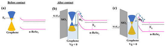
Figure 6.
(a) Band diagram of graphene and ReSe2 before contact, (b) after contact when Vg < 0, and (c) after contact when Vg > 0.
3.5. Gr/ReSe2 Heterostructure as NO2 Gas Sensor
To demonstrate the NO2 gas sensing experiment, the prepared devices were placed in a mass flow controller (MFC) setup as illustrated in Figure S5. Individual Gr, ReSe2, and Gr/ReSe2 heterostructure devices were evaluated at room temperature under different gas concentrations (20–200 ppb). During the gas sensing experiment, the samples were continuously irradiated by a light illumination of 532 nm as it improves gas sensing response [26]. Additionally, the samples were irradiated by visible light instead of UV to avoid any damage from the light source. Figure 7a illustrates the gas sensing dynamic response of Gr/ReSe2 heterostructure under various NO2 concentrations at Vds = 1 V and incident light illumination of 532 nm with the intensity of 310 mW cm−2. The gas sensing response was determined by the following relation:
where “Rg” and “Ra” indicate device resistance under NO2 gas environment and in air. Noteworthy, since two-dimensional materials (2D) bestow a large surface-to-volume ratio, their heterostructure could demonstrate a relatively high NO2 gas sensing response despite being under low NO2 concentration. It is obvious from Figure 7a that the Gr/ReSe2 heterostructure demonstrates a monotonically increasing gas sensing response with rising NO2 concentration from 20 to 200 ppb. Compared to previous reports on 2D materials-based gas sensors, our heterostructure demonstrates a large response of ~36% even at a low NO2 concentration of 20 ppb [64,65,66]. Moving further, we have explored our heterostructure gas sensing response for various light intensities. Under NO2 gas flow (200 ppb) and light wavelength (532 nm) exposure, the gas sensing response of heterostructure was evaluated with increasing light intensities as illustrated in Figure 7b. The gas sensing response rises from ~10% to ~200% as the light intensity increases from 0 to 310 mW cm−2. This is ascribed to the fact that more electrons are produced by increasing light intensity and made their way from the heterojunction to the NO2, subsequently leading to improved gas sensing response. Here, it is also noted that only Gr (black curve), and individual ReSe2 (blue curve) devices have demonstrated lower gas sensing performance of about ~20%, and ~41% as compared to Gr/ReSe2 heterostructure (~200%; red curve) under similar conditions as illustrated in Figure S6. This is attributed to enhanced electron-hole pairs generation at heterojunction interface under light exposure and agrees well with previous reports [67,68]. To further evaluate the NO2 gas response efficiency of the prepared Gr/ReSe2 heterostructure, the transient response was determined for 200 ppb NO2 concentration and under light illumination (532 nm) with intensity 310 mW cm−2 as displayed in Figure S7. As-calculated room temperature NO2 response/recovery time for the heterostructure was found to be 39/126 sec which is comparable with the top gas sensors based on 2D materials so far [69,70]. Next, the Gr/ReSe2 heterostructure was tested for gas sensing stability as illustrated in Figure 7c. The freshly prepared heterostructure (0-day) was placed under NO2 (200 ppb) and light wavelength (532 nm) with an intensity of 310 mW cm−2 exposure. The resultant NO2 gas sensing response was around ~200%. The device was tested again after a month under ambient conditions. The resultant gas sensing response was ~180% which is only 20% less than the original value, revealing the highly stable nature of Gr/ReSe2 heterojunction. Furthermore, to see the stable working potential of prepared sensor, relative humidity effect on response factor was tested as demonstrated in Figure S8. The results reveal similar sensing response under various humidity conditions, i.e., relative humidity (RH: 20–80%). The minor degradation was observed for RH = 20% and RH = 80%, however, no significant change was observed for RH: 40%, 60%, which is typical working conditions in most of the laborites. The results indicate that humidity is not the main factor for consideration to demonstrate consistent NO2 gas sensing behavior. Other parameters, such as NO2 gas exposure, light wavelength and intensity and exposure duration are the main factors that influence sensor properties.
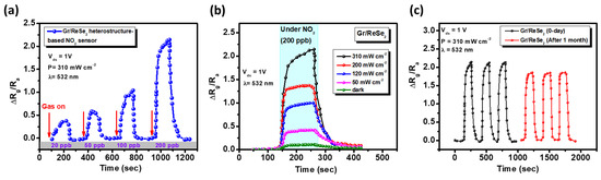
Figure 7.
(a) Dynamic response of Gr/ReSe2 heterostructure under NO2 exposure with different concentrations at Vds = 1V and laser light (532 nm) of power intensity 310 mW cm−2. (b) NO2 (200 ppb) gas sensing response of heterostructure under light wavelength (532 nm) exposure with increasing power intensity. (c) Heterostructure stability assessment under NO2 (200 ppb) with laser light (532 nm) intensity of 310 mW cm−2. The black curve (0-day) indicates the gas sensing performance of freshly prepared heterostructure, whereas the red curve demonstrates heterostructure performance after one month under ambient conditions.

Table 1.
Comparison of photodetector performance of as-prepared FL-ReSe2 and Gr/ReSe2-HS with other reports from the literature.
Table 1.
Comparison of photodetector performance of as-prepared FL-ReSe2 and Gr/ReSe2-HS with other reports from the literature.
| Photodetector (Material) | Responsivity (AW−1) @ Wavelength | Internal or External Quantum Efficiency (%) | Detectivity (Jones) | Rise/Fall Time (s) OR Response Time | Refs. |
|---|---|---|---|---|---|
| Graphene | 5 × 10⁻⁴ | 6–16% | - | - | [71] |
| Few layer ReS2 | 13 (220 nm) | 0.73 | - | 6/21 | [22] |
| 1D Se–2D InSe heterojunction | 3.2 × 10⁻² (460 nm) | 8.7 | 1.7 × 10¹¹ | 3.0 × 10⁻²/3.7 × 10−2 | [72] |
| BP/InSe | 1.17 × 10⁻² (455 nm) | 3.2 | - | 2.4 × 10⁻²/3.2 × 10−2 | [73] |
| Se-ReS2 | 36 (370 nm) | - | 8 × 10¹² | <1 × 10⁻²/<1 × 10−2 | [74] |
| CVD monolayer ReS2 | 13 (532 nm) | - | - | 30-50 s | [75] |
| ReSe2/WSe2 | 0.28 (520 nm) | - | 1.1 × 10¹² | 4.7 × 10⁻³/4.1 × 10−3 | [76] |
| ReS2/ReSe2 | 126.56 (350 nm) | - | 1.76 × 10¹¹ | 6.0 × 10⁻⁶/8.9 × 10−6 | [77] |
| Sb2Se3/WS2 | 1.51 (520 nm) | - | 1.16 × 10¹⁰ | 8.0 × 10⁻³/8.0 × 10−3 | [78] |
| ReS2 bi-layer film | 4 × 10⁻³ (500 nm) | 0.99 | - | 103 | [79] |
| FL-ReSe2 | 11.2 (532 nm) | 26.1 | 1.02 × 10¹⁰ | 2.37/5.03 | This work |
| Gr/ReSe2-HS | 74 (532 nm) | 173 | 1.25 × 10¹¹ | 75 × 10−6/3.0 × 10−6 | This work |
4. Conclusions
We have successfully fabricated Gr/ReSe2 van der Waals heterostructure (vdW-HS) using CVD-grown monolayer graphene (patterned into a rectangular bar), mechanically exfoliated few-layer ReSe2 and all-dry PDMS stamp-assisted transfer method. The prepared HS has been used to evaluate electro-optical properties and gas sensing performance. By exploiting narrow bandgap features of ReSe2, the prepared Gr/ReSe2-HS demonstrated an excellent mobility of 380 cm2/Vs, current on/off ratio ~ 104, photoresponsivity (R ~ 74 AW−1 @ 82 mW cm−2), detectivity (D* ~ 1.25 × 10¹¹ Jones), external quantum efficiency (EQE ~ 173%) and rapid photoresponse (rise/fall time ~ 75/3 µs) as compared to individual ReSe2 device (mobility = 36 cm2 V−1s−1, Ion/Ioff ratio = 1.4 × 10⁵–1.8 × 10⁵, R = 11.2 AW−1, D* = 1.02 × 10¹⁰, EQE ~ 26.1%, rise/fall time = 2.37/5.03 s). Such remarkable performance is due to the combined result of strong light absorption of ReSe2 and high carrier transport of graphene. Moreover, low value of Schottky barrier height (SBH) for Gr/ReSe2-HS (9.02 meV @ Vbg = 40 V) confirms that graphene is somehow working as defects (due to Si/SiO2 dielectric substrate) suppressing layer. Furthermore, the HS was subjected to NO2 gas environment under various humidity conditions to test its aptitude for the gas sensor at room temperature (26.85 °C). The results demonstrated a high response, good reversibility, and gas selectivity under light irradiation of 532 nm. Interestingly, the proposed HS has illustrated an excellent response even toward low ppb-level NO2 exposure (20 ppb), revealing the proposed HS is superior to most of the reported literature. To conclude, our Gr/ReSe2-HS is capable of demonstrating excellent electro-optical as well as gas sensing performance simultaneously and, therefore, can be used as a building block to fabricate next-generation photodetectors and gas sensors to further enhance optoelectronics research domain and internet of things (IoT) devices. Moreover, it offers a potential sensing platform for cost-effective environmental monitoring systems.
Supplementary Materials
The following supporting information can be downloaded at: https://www.mdpi.com/article/10.3390/nano12213713/s1, Figure S1: Gr/ReSe2 heterostructure fabrication step-by-step detail; Figure S2: (a) AFM image (scale bar: 3 µm), and (b) corresponding height profile to accurately assess ReSe2 flake thickness; Figure S3: (a) Transfer characteristics (Ids–Vbg) of mono-layer graphene measured at Vds = 0.1 V reveals CNP = −8 V. (b) Output characteristics (Ids–Vds) calculated at various Vbg from −40 to 50 V reveal ohmic behavior of monolayer grapheme; Figure S4: Photocurrent measurement of ReSe2-based photodetector at mentioned conditions; Figure S5: MFC (mass flow controller) setup to test individual flakes (Gr, and ReSe2) and Gr/ReSe2 heterostructure-based NO2 gas sensing performance; Figure S6: Room temperature comparative analysis of Gas sensing responses from individual Gr (black), individual ReSe2 (blue), and Gr/ReSe2 heterostructure (red) for NO2 (200 ppb) under laser power of 310 mW cm−2 with a wavelength of 532 nm; Figure S7: Room temperature transient response of Gr/ReSe2 heterostructure for NO2 (200 ppb) under laser power of 310 mW cm−2 with a wavelength of 532 nm; Figure S8: (a) Response factor of Gr/ReSe2-HS for 200 ppm NO2 exposure under different values of relative humidity. (b) Corresponding column bar representation of the maximum value of response factor of Figure S8a.
Author Contributions
Conceptualization, K.H.; Data curation, A.R.; Formal analysis, S.H., K.H. and M.A.A.; Investigation, A.R., S.H. and M.I.; Methodology, S.A.P. and M.A.U.D.; Resources, M.I. and M.A.U.D.; Software, S.A.P.; Supervision, G.N.; Visualization, O.H.; Writing—review & editing, M.A.A. All authors have read and agreed to the published version of the manuscript.
Funding
This research project was supported by Sejong University, Seoul 05006, Korea, and all the authors are thankful for this support.
Institutional Review Board Statement
Not applicable.
Informed Consent Statement
Not applicable.
Data Availability Statement
The data can be requested from corresponding author upon reasonsble request.
Conflicts of Interest
The authors declare no conflict of interest.
References
- Cheng, Z.; Cao, R.; Wei, K.; Yao, Y.; Liu, X.; Kang, J.; Dong, J.; Shi, Z.; Zhang, H.; Zhang, X. 2D Materials Enabled Next-Generation Integrated Optoelectronics: From Fabrication to Applications. Adv. Sci. 2021, 8, 2003834. [Google Scholar] [CrossRef] [PubMed]
- Liu, S.; Wang, J.; Shao, J.; Ouyang, D.; Zhang, W.; Liu, S.; Li, Y.; Zhai, T. Nanopatterning Technologies of Two-Dimensional Materials for Integrated Electronic and Optoelectronic Devices. Adv. Mater. 2022, 2200734. [Google Scholar] [CrossRef] [PubMed]
- Yu, W.; Gong, K.; Li, Y.; Ding, B.; Li, L.; Xu, Y.; Wang, R.; Li, L.; Zhang, G.; Lin, S. Flexible 2D Materials beyond Graphene: Synthesis, Properties, and Applications. Small 2022, 18, 2105383. [Google Scholar] [CrossRef] [PubMed]
- Wu, R.; Tao, Q.; Dang, W.; Liu, Y.; Li, B.; Li, J.; Zhao, B.; Zhang, Z.; Ma, H.; Sun, G. van der Waals epitaxial growth of atomically thin 2D metals on dangling-bond-free WSe2 and WS2. Adv. Funct. Mater. 2019, 29, 1806611. [Google Scholar] [CrossRef]
- Yin, X.; Tang, C.S.; Zheng, Y.; Gao, J.; Wu, J.; Zhang, H.; Chhowalla, M.; Chen, W.; Wee, A.T. Recent developments in 2D transition metal dichalcogenides: Phase transition and applications of the (quasi-) metallic phases. Chem. Soc. Rev. 2021, 50, 10087–10115. [Google Scholar] [CrossRef]
- Ping, J.; Fan, Z.; Sindoro, M.; Ying, Y.; Zhang, H. Recent advances in sensing applications of two-dimensional transition metal dichalcogenide nanosheets and their composites. Adv. Funct. Mater. 2017, 27, 1605817. [Google Scholar] [CrossRef]
- Zhang, Y.; Yao, Y.; Sendeku, M.G.; Yin, L.; Zhan, X.; Wang, F.; Wang, Z.; He, J. Recent progress in CVD growth of 2D transition metal dichalcogenides and related heterostructures. Adv. Mater. 2019, 31, 1901694. [Google Scholar] [CrossRef]
- Huo, N.; Konstantatos, G. Recent progress and future prospects of 2D-based photodetectors. Adv. Mater. 2018, 30, 1801164. [Google Scholar] [CrossRef]
- Guan, X.; Yu, X.; Periyanagounder, D.; Benzigar, M.R.; Huang, J.K.; Lin, C.H.; Kim, J.; Singh, S.; Hu, L.; Liu, G. Recent progress in short-to long-wave infrared photodetection using 2D materials and heterostructures. Adv. Opt. Mater. 2021, 9, 2001708. [Google Scholar] [CrossRef]
- Rehman, A.; Park, S.-J. State of the art two-dimensional materials-based photodetectors: Prospects, challenges and future outlook. J. Ind. Eng. Chem. 2020, 89, 28–46. [Google Scholar] [CrossRef]
- Lin, L.; Lei, W.; Zhang, S.; Liu, Y.; Wallace, G.G.; Chen, J. Two-dimensional transition metal dichalcogenides in supercapacitors and secondary batteries. Energy Storage Mater. 2019, 19, 408–423. [Google Scholar] [CrossRef]
- Yan, P.; Yang, D.; Wang, H.; Yang, S.; Ge, Z. Recent advances in dopant-free organic hole-transporting materials for efficient, stable and low-cost perovskite solar cells. Energy Environ. Sci. 2022, 15, 3630–3669. [Google Scholar] [CrossRef]
- Zheng, W.; Liu, X.; Xie, J.; Lu, G.; Zhang, J. Emerging van der Waals junctions based on TMDs materials for advanced gas sensors. Coord. Chem. Rev. 2021, 447, 214151. [Google Scholar] [CrossRef]
- Tajik, S.; Dourandish, Z.; Nejad, F.G.; Beitollahi, H.; Jahani, P.M.; Di Bartolomeo, A. Transition metal dichalcogenides: Synthesis and use in the development of electrochemical sensors and biosensors. Biosens. Bioelectron. 2022, 216, 114674. [Google Scholar] [CrossRef]
- Mathew, M.; Radhakrishnan, S.; Vaidyanathan, A.; Chakraborty, B.; Rout, C.S. Flexible and wearable electrochemical biosensors based on two-dimensional materials: Recent developments. Anal. Bioanal. Chem. 2021, 413, 727–762. [Google Scholar] [CrossRef] [PubMed]
- Rohaizad, N.; Mayorga-Martinez, C.C.; Sofer, Z.K.; Pumera, M. 1T-phase transition metal dichalcogenides (MoS2, MoSe2, WS2, and WSe2) with fast heterogeneous electron transfer: Application on second-generation enzyme-based biosensor. ACS Appl. Mater. Interfaces 2017, 9, 40697–40706. [Google Scholar] [CrossRef]
- Xiao, M.; Wei, S.; Chen, J.; Tian, J.; Brooks, C.L., III; Marsh, E.N.G.; Chen, Z. Molecular mechanisms of interactions between monolayered transition metal dichalcogenides and biological molecules. J. Am. Chem. Soc. 2019, 141, 9980–9988. [Google Scholar] [CrossRef]
- Lim, H.R.; Kim, H.S.; Qazi, R.; Kwon, Y.T.; Jeong, J.W.; Yeo, W.H. Advanced soft materials, sensor integrations, and applications of wearable flexible hybrid electronics in healthcare, energy, and environment. Adv. Mater. 2020, 32, 1901924. [Google Scholar] [CrossRef]
- Jang, M.S.; Kim, H.; Son, Y.-W.; Atwater, H.A.; Goddard, W.A., III. Graphene field effect transistor without an energy gap. Proc. Natl. Acad. Sci. USA 2013, 110, 8786–8789. [Google Scholar] [CrossRef]
- Pham, T.; Li, G.; Bekyarova, E.; Itkis, M.E.; Mulchandani, A. MoS2-based optoelectronic gas sensor with sub-parts-per-billion limit of NO2 gas detection. ACS Nano 2019, 13, 3196–3205. [Google Scholar] [CrossRef]
- Kim, S.; Shin, D.H.; Kim, Y.-S.; Lee, I.H.; Lee, C.-W.; Seo, S.; Jung, S. Highly Efficient Experimental Approach to Evaluate Metal to 2D Semiconductor Interfaces in Vertical Diodes with Asymmetric Metal Contacts. ACS Appl. Mater. Interfaces 2021, 13, 27705–27712. [Google Scholar] [CrossRef] [PubMed]
- Nazir, G.; Rehman, M.A.; Khan, M.F.; Dastgeer, G.; Aftab, S.; Afzal, A.M.; Seo, Y.; Eom, J. Comparison of electrical and photoelectrical properties of ReS2 field-effect transistors on different dielectric substrates. ACS Appl. Mater. Interfaces 2018, 10, 32501–32509. [Google Scholar] [CrossRef]
- Kim, J.; Heo, K.; Kang, D.H.; Shin, C.; Lee, S.; Yu, H.Y.; Park, J.H. Rhenium Diselenide (ReSe2) Near-Infrared Photodetector: Performance Enhancement by Selective p-Doping Technique. Adv. Sci. 2019, 6, 1901255. [Google Scholar] [CrossRef] [PubMed]
- Kang, B.; Kim, Y.; Yoo, W.J.; Lee, C. Ultrahigh photoresponsive device based on ReS2/graphene heterostructure. Small 2018, 14, 1802593. [Google Scholar] [CrossRef] [PubMed]
- Ma, H.; Xing, Y.; Han, J.; Cui, B.; Lei, T.; Tu, H.; Guan, B.; Zeng, Z.; Zhang, B.; Lv, W. Ultrasensitive and Broad-Spectrum Photodetectors Based on InSe/ReS2 Heterostructure. Adv. Opt. Mater. 2022, 10, 2101772. [Google Scholar] [CrossRef]
- Niu, Y.; Zeng, J.; Liu, X.; Li, J.; Wang, Q.; Li, H.; de Rooij, N.F.; Wang, Y.; Zhou, G. A Photovoltaic Self-Powered Gas Sensor Based on All-Dry Transferred MoS2/GaSe Heterojunction for ppb-Level NO2 Sensing at Room Temperature. Adv. Sci. 2021, 8, 2100472. [Google Scholar] [CrossRef] [PubMed]
- Kufer, D.; Nikitskiy, I.; Lasanta, T.; Navickaite, G.; Koppens, F.H.; Konstantatos, G. Hybrid 2D–0D MoS2–PbS quantum dot photodetectors. Adv. Mater. 2015, 27, 176–180. [Google Scholar] [CrossRef]
- Nazir, G.; Khan, M.F.; Akhtar, I.; Akbar, K.; Gautam, P.; Noh, H.; Seo, Y.; Chun, S.-H.; Eom, J. Enhanced photoresponse of ZnO quantum dot-decorated MoS2 thin films. RSC Adv. 2017, 7, 16890–16900. [Google Scholar] [CrossRef]
- Mallick, A.; Visoly-Fisher, I. Pb in halide perovskites for photovoltaics: Reasons for optimism. Mater. Adv. 2021, 2, 6125–6135. [Google Scholar] [CrossRef]
- Lan, C.; Li, C.; Wang, S.; He, T.; Zhou, Z.; Wei, D.; Guo, H.; Yang, H.; Liu, Y. Highly responsive and broadband photodetectors based on WS2–graphene van der Waals epitaxial heterostructures. J. Mater. Chem. C 2017, 5, 1494–1500. [Google Scholar] [CrossRef]
- Yu, W.; Li, S.; Zhang, Y.; Ma, W.; Sun, T.; Yuan, J.; Fu, K.; Bao, Q. Near-infrared photodetectors based on MoTe2/graphene heterostructure with high responsivity and flexibility. Small 2017, 13, 1700268. [Google Scholar] [CrossRef] [PubMed]
- Liang, S.J.; Cheng, B.; Cui, X.; Miao, F. Van der Waals heterostructures for high-performance device applications: Challenges and opportunities. Adv. Mater. 2020, 32, 1903800. [Google Scholar] [CrossRef] [PubMed]
- Darmadi, I.; Nugroho, F.A.A.; Langhammer, C. High-performance nanostructured palladium-based hydrogen sensors—Current limitations and strategies for their mitigation. ACS Sens. 2020, 5, 3306–3327. [Google Scholar] [CrossRef] [PubMed]
- Feng, Q.; Huang, B.; Li, X. Graphene-Based Heterostructure Composite Sensing Materials for Detection of Nitrogen-Containing Harmful Gases. Adv. Funct. Mater. 2021, 31, 2104058. [Google Scholar] [CrossRef]
- Korotcenkov, G. Metal oxides for solid-state gas sensors: What determines our choice? Mater. Sci. Eng. B 2007, 139, 1–23. [Google Scholar] [CrossRef]
- Saruhan, B.; Lontio Fomekong, R.; Nahirniak, S. Influences of semiconductor metal oxide properties on gas sensing characteristics. Front. Sens. 2021, 2, 657931. [Google Scholar] [CrossRef]
- Yang, S.; Tongay, S.; Li, Y.; Yue, Q.; Xia, J.-B.; Li, S.-S.; Li, J.; Wei, S.-H. Layer-dependent electrical and optoelectronic responses of ReSe2 nanosheet transistors. Nanoscale 2014, 6, 7226–7231. [Google Scholar] [CrossRef]
- Gusakova, J.; Wang, X.; Shiau, L.L.; Krivosheeva, A.; Shaposhnikov, V.; Borisenko, V.; Gusakov, V.; Tay, B.K. Electronic properties of bulk and monolayer TMDs: Theoretical study within DFT framework (GVJ-2e method). Physica Status Solidi (a) 2017, 214, 1700218. [Google Scholar] [CrossRef]
- Bach, T.P.-A.; Jaffery, S.H.A.; Nguyen, D.C.; Ali, A.; Hussain, S.; Hussain, M.; Seo, Y.; Jung, J. Schottky barrier height modulation and photoconductivity in a vertical graphene/ReSe2 vdW pn heterojunction barristor. J. Mater. Res. Technol. 2022, 17, 2796–2806. [Google Scholar] [CrossRef]
- Dean, C.R.; Young, A.F.; Meric, I.; Lee, C.; Wang, L.; Sorgenfrei, S.; Watanabe, K.; Taniguchi, T.; Kim, P.; Shepard, K.L. Boron nitride substrates for high-quality graphene electronics. Nat. Nanotechnol. 2010, 5, 722–726. [Google Scholar] [CrossRef]
- Zhao, H.; Wu, J.; Zhong, H.; Guo, Q.; Wang, X.; Xia, F.; Yang, L.; Tan, P.; Wang, H. Interlayer interactions in anisotropic atomically thin rhenium diselenide. Nano Res. 2015, 8, 3651–3661. [Google Scholar] [CrossRef]
- Wolverson, D.; Crampin, S.; Kazemi, A.S.; Ilie, A.; Bending, S.J. Raman spectra of monolayer, few-layer, and bulk ReSe2: An anisotropic layered semiconductor. ACS Nano 2014, 8, 11154–11164. [Google Scholar] [CrossRef] [PubMed]
- Nazir, G.; Khan, M.F.; Aftab, S.; Afzal, A.M.; Dastgeer, G.; Rehman, M.A.; Seo, Y.; Eom, J. Gate tunable transport in Graphene/MoS2/(Cr/Au) vertical field-effect transistors. Nanomaterials 2017, 8, 14. [Google Scholar] [CrossRef] [PubMed]
- Faella, E.; Intonti, K.; Viscardi, L.; Giubileo, F.; Kumar, A.; Lam, H.T.; Anastasiou, K.; Craciun, M.F.; Russo, S.; Di Bartolomeo, A. Electric Transport in Few-Layer ReSe2 Transistors Modulated by Air Pressure and Light. Nanomaterials 2022, 12, 1886. [Google Scholar] [CrossRef] [PubMed]
- Nazir, G.; Khan, M.F.; Iermolenko, V.M.; Eom, J. Two-and four-probe field-effect and Hall mobilities in transition metal dichalcogenide field-effect transistors. RSC Adv. 2016, 6, 60787–60793. [Google Scholar] [CrossRef]
- Iqbal, M.W.; Iqbal, M.Z.; Khan, M.F.; Shehzad, M.A.; Seo, Y.; Park, J.H.; Hwang, C.; Eom, J. High-mobility and air-stable single-layer WS2 field-effect transistors sandwiched between chemical vapor deposition-grown hexagonal BN films. Sci. Rep. 2015, 5, 10699. [Google Scholar] [CrossRef]
- Khan, M.F.; Rehman, S.; Akhtar, I.; Aftab, S.; Ajmal, H.M.S.; Khan, W.; Kim, D.-k.; Eom, J. High mobility ReSe2 field effect transistors: Schottky-barrier-height-dependent photoresponsivity and broadband light detection with Co decoration. 2D Mater. 2019, 7, 015010. [Google Scholar] [CrossRef]
- Kaushal, P.; Khanna, G. The role of 2-Dimensional materials for electronic devices. Mater. Sci. Semicond. Process. 2022, 143, 106546. [Google Scholar] [CrossRef]
- Wang, X.; Huang, L.; Peng, Y.; Huo, N.; Wu, K.; Xia, C.; Wei, Z.; Tongay, S.; Li, J. Enhanced rectification, transport property and photocurrent generation of multilayer ReSe2/MoS2 p–n heterojunctions. Nano Res. 2016, 9, 507–516. [Google Scholar]
- Jang, A.-R.; Jeon, E.K.; Kang, D.; Kim, G.; Kim, B.-S.; Kang, D.J.; Shin, H.S. Reversibly light-modulated dirac point of graphene functionalized with spiropyran. ACS Nano 2012, 6, 9207–9213. [Google Scholar] [CrossRef]
- Chin, H.-T.; Lee, J.-J.; Hofmann, M.; Hsieh, Y.-P. Impact of growth rate on graphene lattice-defect formation within a single crystalline domain. Sci. Rep. 2018, 8, 4046. [Google Scholar] [CrossRef] [PubMed]
- Gupta, S.; Kumar, R. Photodetection Properties of Graphene/Silicon van der Waals Heterojunction. ECS J. Solid State Sci. Technol. 2022, 11, 061010. [Google Scholar] [CrossRef]
- Nalwa, H.S. A review of molybdenum disulfide (MoS2) based photodetectors: From ultra-broadband, self-powered to flexible devices. RSC Adv. 2020, 10, 30529–30602. [Google Scholar] [CrossRef] [PubMed]
- Zheng, Y.; Tang, X.; Wang, W.; Jin, L.; Li, G. Large-Size Ultrathin α-Ga2S3 Nanosheets toward High-Performance Photodetection. Adv. Funct. Mater. 2021, 31, 2008307. [Google Scholar] [CrossRef]
- Chen, J.; Ouyang, W.; Yang, W.; He, J.H.; Fang, X. Recent progress of heterojunction ultraviolet photodetectors: Materials, integrations, and applications. Adv. Funct. Mater. 2020, 30, 1909909. [Google Scholar] [CrossRef]
- Li, M.Y.; Yu, M.; Su, D.; Zhang, J.; Jiang, S.; Wu, J.; Wang, Q.; Liu, S. Ultrahigh responsivity UV photodetector based on Cu nanostructure/ZnO QD hybrid architectures. Small 2019, 15, 1901606. [Google Scholar] [CrossRef]
- Mao, Y.; Xu, P.; Wu, Q.; Xiong, J.; Peng, R.; Huang, W.; Chen, S.; Wu, Z.; Li, C. Self-powered high-detectivity lateral MoS2 Schottky photodetectors for near-infrared operation. Adv. Electron. Mater. 2021, 7, 2001138. [Google Scholar] [CrossRef]
- Pollmann, E.; Sleziona, S.; Foller, T.; Hagemann, U.; Gorynski, C.; Petri, O.; Madauß, L.; Breuer, L.; Schleberger, M. Large-Area, Two-Dimensional MoS2 Exfoliated on Gold: Direct Experimental Access to the Metal–Semiconductor Interface. ACS Omega 2021, 6, 15929–15939. [Google Scholar] [CrossRef]
- Lee, S.Y.; Kim, U.J.; Chung, J.; Nam, H.; Jeong, H.Y.; Han, G.H.; Kim, H.; Oh, H.M.; Lee, H.; Kim, H. Large work function modulation of monolayer MoS2 by ambient gases. ACS Nano 2016, 10, 6100–6107. [Google Scholar] [CrossRef]
- Gupta, S.; Rortais, F.; Ohshima, R.; Ando, Y.; Endo, T.; Miyata, Y.; Shiraishi, M. Monolayer MoS2 field effect transistor with low Schottky barrier height with ferromagnetic metal contacts. Sci. Rep. 2019, 9, 17032. [Google Scholar] [CrossRef]
- Urban, F.; Martucciello, N.; Peters, L.; McEvoy, N.; Di Bartolomeo, A. Environmental effects on the electrical characteristics of back-gated WSe2 field-effect transistors. Nanomaterials 2018, 8, 901. [Google Scholar] [CrossRef]
- Yu, Y.-J.; Zhao, Y.; Ryu, S.; Brus, L.E.; Kim, K.S.; Kim, P. Tuning the graphene work function by electric field effect. Nano Lett. 2009, 9, 3430–3434. [Google Scholar] [CrossRef] [PubMed]
- Jahangir, I.; Uddin, M.A.; Singh, A.K.; Koley, G.; Chandrashekhar, M. Richardson constant and electrostatics in transfer-free CVD grown few-layer MoS2/graphene barristor with Schottky barrier modulation > 0.6 eV. Appl. Phys. Lett. 2017, 111, 142101. [Google Scholar] [CrossRef]
- Kumar, S.; Pavelyev, V.; Mishra, P.; Tripathi, N.; Sharma, P.; Calle, F. A review on 2D transition metal di-chalcogenides and metal oxide nanostructures based NO2 gas sensors. Mater. Sci. Semicond. Process. 2020, 107, 104865. [Google Scholar] [CrossRef]
- Guo, R.; Han, Y.; Su, C.; Chen, X.; Zeng, M.; Hu, N.; Su, Y.; Zhou, Z.; Wei, H.; Yang, Z. Ultrasensitive room temperature NO2 sensors based on liquid phase exfoliated WSe2 nanosheets. Sens. Actuators B Chem. 2019, 300, 127013. [Google Scholar] [CrossRef]
- Chen, X.; Hu, J.; Chen, P.; Yin, M.; Meng, F.; Zhang, Y. UV-light-assisted NO2 gas sensor based on WS2/PbS heterostructures with full recoverability and reliable anti-humidity ability. Sens. Actuators B Chem. 2021, 339, 129902. [Google Scholar] [CrossRef]
- Yang, Z.; Zhang, D.; Chen, H. MOF-derived indium oxide hollow microtubes/MoS2 nanoparticles for NO2 gas sensing. Sens. Actuators B Chem. 2019, 300, 127037. [Google Scholar] [CrossRef]
- Zheng, W.; Xu, Y.; Zheng, L.; Yang, C.; Pinna, N.; Liu, X.; Zhang, J. MoS2 Van der Waals p–n junctions enabling highly selective room-temperature NO2 sensor. Adv. Funct. Mater. 2020, 30, 2000435. [Google Scholar] [CrossRef]
- Kim, Y.; Kwon, K.C.; Kang, S.; Kim, C.; Kim, T.H.; Hong, S.-P.; Park, S.Y.; Suh, J.M.; Choi, M.-J.; Han, S. Two-dimensional NbS2 gas sensors for selective and reversible NO2 detection at room temperature. ACS Sens. 2019, 4, 2395–2402. [Google Scholar] [CrossRef]
- Li, W.; Zhang, Y.; Long, X.; Cao, J.; Xin, X.; Guan, X.; Peng, J.; Zheng, X. Gas sensors based on mechanically exfoliated MoS2 nanosheets for room-temperature NO2 detection. Sensors 2019, 19, 2123. [Google Scholar] [CrossRef]
- Xia, F.; Mueller, T.; Lin, Y.-m.; Valdes-Garcia, A.; Avouris, P. Ultrafast graphene photodetector. Nat. Nanotechnol. 2009, 4, 839–843. [Google Scholar] [CrossRef] [PubMed]
- Shang, H.; Chen, H.; Dai, M.; Hu, Y.; Gao, F.; Yang, H.; Xu, B.; Zhang, S.; Tan, B.; Zhang, X. A mixed-dimensional 1D Se–2D InSe van der Waals heterojunction for high responsivity self-powered photodetectors. Nanoscale Horiz. 2020, 5, 564–572. [Google Scholar] [CrossRef] [PubMed]
- Zhao, S.; Wu, J.; Jin, K.; Ding, H.; Li, T.; Wu, C.; Pan, N.; Wang, X. Highly Polarized and Fast Photoresponse of Black Phosphorus-InSe Vertical p–n Heterojunctions. Adv. Funct. Mater. 2018, 28, 1802011. [Google Scholar] [CrossRef]
- Qin, J.K.; Qiu, G.; He, W.; Jian, J.; Si, M.W.; Duan, Y.Q.; Charnas, A.; Zemlyanov, D.Y.; Wang, H.Y.; Shao, W.Z. Epitaxial growth of 1D atomic chain based Se nanoplates on monolayer ReS2 for high-performance photodetectors. Adv. Funct. Mater. 2018, 28, 1806254. [Google Scholar] [CrossRef]
- Li, X.; Cui, F.; Feng, Q.; Wang, G.; Xu, X.; Wu, J.; Mao, N.; Liang, X.; Zhang, Z.; Zhang, J. Controlled growth of large-area anisotropic ReS2 atomic layer and its photodetector application. Nanoscale 2016, 8, 18956–18962. [Google Scholar] [CrossRef]
- Tian, X.; Liu, Y. Van der Waals heterojunction ReSe2/WSe2 polarization-resolved photodetector. J. Semicond. 2021, 42, 032001. [Google Scholar] [CrossRef]
- Li, K.; Du, C.; Gao, H.; Yin, T.; Zheng, L.; Leng, J.; Wang, W. Ultrafast and Polarization-Sensitive ReS2/ReSe2 Heterostructure Photodetectors with Ambipolar Photoresponse. ACS Appl. Mater. Interfaces 2022, 14, 33589–33597. [Google Scholar] [CrossRef]
- Sun, G.; Li, B.; Li, J.; Zhang, Z.; Ma, H.; Chen, P.; Zhao, B.; Wu, R.; Dang, W.; Yang, X. Direct van der Waals epitaxial growth of 1D/2D Sb2Se3/WS2 mixed-dimensional pn heterojunctions. Nano Res. 2019, 12, 1139–1145. [Google Scholar] [CrossRef]
- Hafeez, M.; Gan, L.; Li, H.; Ma, Y.; Zhai, T. Large-area bilayer ReS2 film/multilayer ReS2 flakes synthesized by chemical vapor deposition for high performance photodetectors. Adv. Funct. Mater. 2016, 26, 4551–4560. [Google Scholar] [CrossRef]


Publisher’s Note: MDPI stays neutral with regard to jurisdictional claims in published maps and institutional affiliations. |
© 2022 by the authors. Licensee MDPI, Basel, Switzerland. This article is an open access article distributed under the terms and conditions of the Creative Commons Attribution (CC BY) license (https://creativecommons.org/licenses/by/4.0/).