Article

Threshold Voltage Adjustment by Varying Ge Content in SiGe p-Channel for Single Metal Shared Gate Complementary FET (CFET)

Department of Engineering and System Science, National Tsing Hua University, Hsinchu 30013, Taiwan
*
Author to whom correspondence should be addressed.
Nanomaterials 2022, 12(20), 3712; https://doi.org/10.3390/nano12203712
Submission received: 8 September 2022 / Revised: 12 October 2022 / Accepted: 19 October 2022 / Published: 21 October 2022
(This article belongs to the Special Issue Nanomaterials for Electron Devices)

Abstract

:
We have demonstrated the method of threshold voltage (VT) adjustment by controlling Ge content in the SiGe p-channel of N1 complementary field-effect transistor (CFET) for conquering the work function metal (WFM) filling issue on highly scaled MOSFET. Single WFM shared gate N1 CFET was used to study and emphasize the VT tunability of the proposed Ge content method. The result reveals that the Ge mole fraction influences VTP of 5 mV/Ge%, and a close result can also be obtained from the energy band configuration of Si1-xGex. Additionally, the single WFM shared gate N1 CFET inverter with VT adjusted by the Ge content method presents a well-designed voltage transfer curve, and its inverter transient response is also presented. Furthermore, the designed CFET inverter is used to construct a well-behaved 6T-SRAM with a large SNM of ~120 mV at VDD of 0.5 V.

1. Introduction

The semiconductor logic device architectures continue to progress, and innovation is driving Moore’s law scaling. Given the transition from planar metal oxide semiconductor field-effect transistor (MOSFET) to three-dimensional FinFET and following stacked nanosheet gate-all-around FET (GAAFETs), the complementary FET (CFET) has been recently proposed as a candidate architecture for the beyond technology node [1,2,3,4]. However, due to shrinking gate length (LG), insufficient space for filling multiple work function metal (WFM), which is used for obtaining the desirable device’s threshold voltage (VT), has become a challenging problem. Since the gate stack also uses space on the sidewalls under the replacement metal gate (RMG) process [5,6,7], the issue could worsen on stacked nanosheet GAAFETs and become more severe with CFETs. That is because the vertical spacing between the channels must also simultaneously be considered for stacked architectures [8]. As for CFETs, the dual WFM gates should be achieved in the same area but in different layers, which increases the issue’s complexity to a greater extent [1,9].
To maintain the flexibility of multi-VT for balancing low power consumption and high performance, volume-less (also called zero-thickness) methods for VT adjustment are needed. Some research focused on finding methods to reduce the thickness of gate stacks while not losing the VT stability [6,7]. Others proposed an alternative way of using a dipole layer to adjust VT due to its role as an intrinsic fixed charge in gate stacks [10,11]. However, the incorporation of the dipole layer may cause an increase of interface trap density [12,13], which would deteriorate the reliability of the device. Furthermore, the dipole layer may also bring the degradation of mobility [10,13]. This paper proposes another alternative method for adjusting VT by controlling the Ge content in the Si1-xGex channel. Si1-xGex is used in strain engineering for hole mobility improvement due to its compatibility in the Si CMOS process [14]. On the other hand, Si1-xGex was proposed to lower PMOS VT by band engineering [15]. In addition, a FinFET CMOS technology of Si NMOS-SiGe PMOS with common WFM was demonstrated [16]. Additionally, decreasing VT was found in Si1-xGex PMOS with increasing Ge content [17]. These studies showed that the Si1-xGex possesses the potential to influence VT. Therefore, in this work, we discuss the methodology of VT adjustment by varying Ge content in the SiGe channel and demonstrate the VT adjustment method on the single WFM shared gate CFET as N1 technology using Sentaurus technology computer-aided design (TCAD). The process on the SiGe channel would have no occupation on the spacing for high-k metal gates and gate contact filling. On the other hand, the SiGe channel with Ge content of less than 50% has already been used in today’s semiconductor technology; hence, the proposed method is compatible with the manufacturing technology. In addition, we present the inverter characteristics of the designed N1 CFET and further use it to construct a 6T-SRAM.

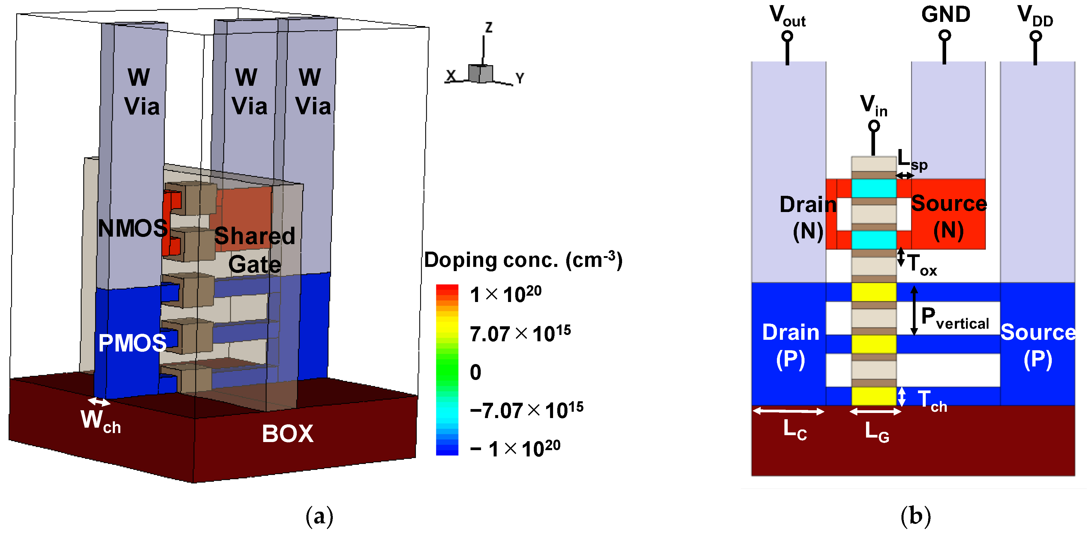
2. Device Structure and Simulation Methodology

Figure 1a displays a bird’s eye view of the N1 CFET architecture in this study. The Synopsys TCAD simulator was employed for the 3-D simulations [18]. The simulation parameters, including gate length (LG = 12 nm), channel thickness (Wch = 6 nm), gate oxide thickness (Tox = 2 nm, HfO2), channel vertical pitch (Pvertical = 14 nm), spacer length (Lsp = 4 nm), and source/drain contact length (LC = 20 nm), are based on the prediction of the 1 nm node logic device in the international roadmap for devices and system (IRDS) 2020 [19].
In the meantime, the architecture designs are also referred from the experimental CFET structure proposed by Intel [1], which stacked the two-channel NMOS on top of the three-channel PMOS on a Si-on-insulator (SOI) substrate. The PMOS is designed to have a longer contact gate pitch (CGP) than the NMOS to separate the source contacts of NMOS and PMOS as the electrodes of GND and VDD for the CFET inverter, respectively. As shown in Figure 1b, the contact of Vin is shared by the NMOS gate and the PMOS gate. In addition, Vout is shared by the NMOS drain and PMOS drain. GND and VDD are used for the sources of NMOS and PMOS, respectively. Tungsten is used as the contact metal for all the electrodes. Afterward, SiO2 is used as fill for oxide passivation, side-wall spacer, and filler of nanosheets inter-spacing. The structural simulation parameters of the N1 CFET simulation are shown in Table 1.
To increase the accuracy of the simulation in this study, the ID-VG transfer characteristics of the CFET with LG of 75 nm were calibrated to the experimental result from [1]. The following physical models were considered and coupled in the TCAD simulation:
  • The drift-diffusion model was included with the coupled Possion’s and continuity equations to determine the electrostatic potential and carrier transport.
  • The density gradient model was included to correct the quantum confinement effect in the drift-diffusion model due to the highly scaled dimension [20].
  • The doping-concentration-dependent Shockley–Read–Hall (SRH) recombination model was included for the generation–recombination mechanism.
  • The Slotboom bandgap narrowing model was included for doping-concentration-dependent bandgap correction [21].
  • The doping-dependent, transverse field dependence, and high-field saturation mobility models were included to consider impurity scattering, interfacial surface roughness scattering, and coulomb scattering degradations.
  • A ballistic mobility model was considered for quasi-ballistic transport.
The calibration result is shown in Figure 2. The simulation of the following inverter transient response and the 6T-SRAM were achieved using “mixed-mode” in SDEVICE of Sentaurus TCAD.

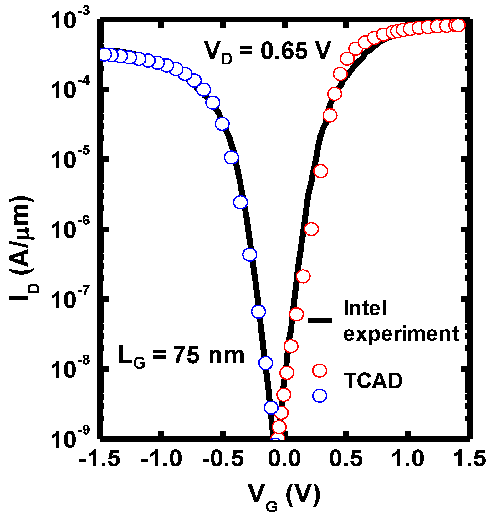
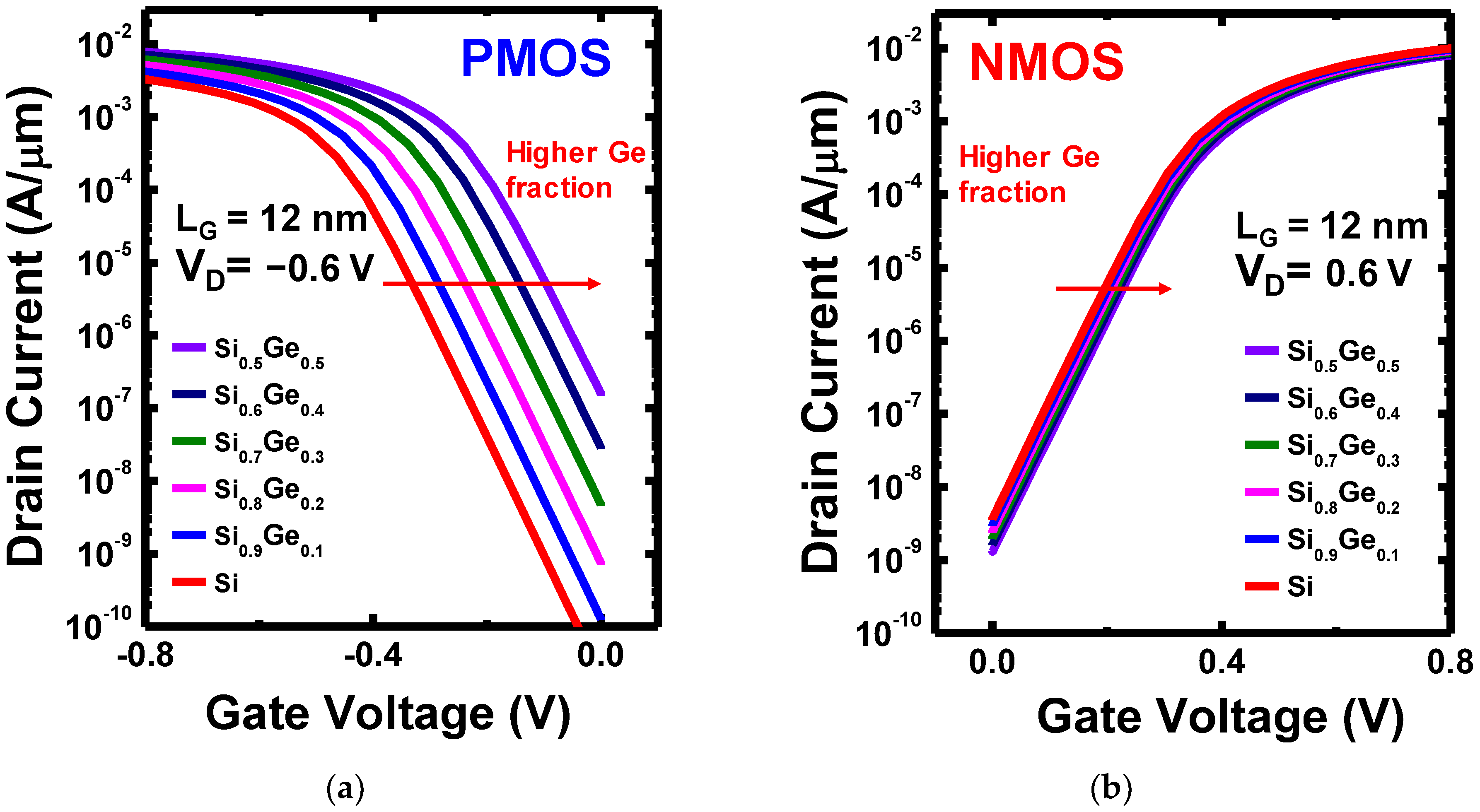
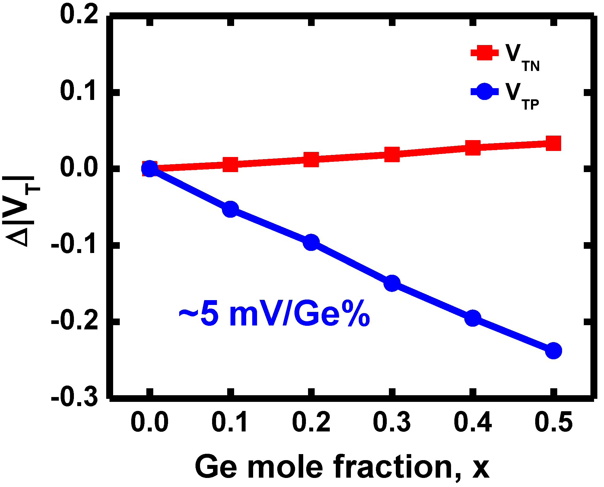
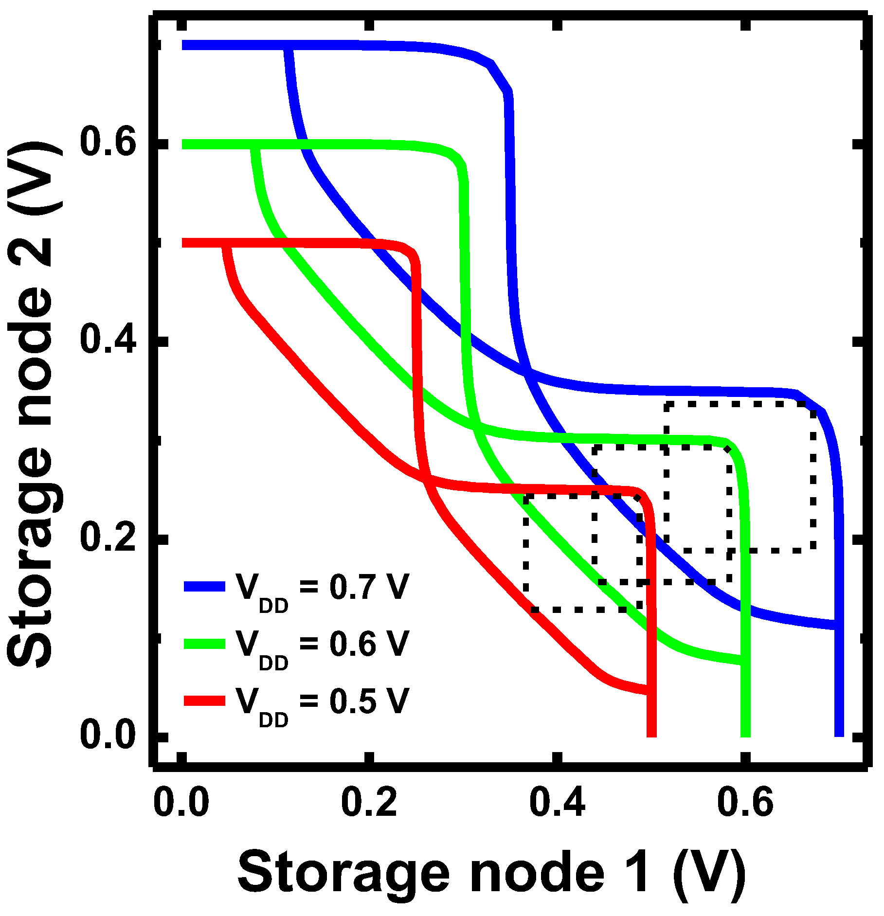
3. Results and Discussion

First, to demonstrate the VT tunability of changing the Ge mole fraction (x) in the Si1-xGex channel for N1 CFET, we analyzed the electrical characteristics of PMOS and NMOS on the Si1-xGex composition in the CFET structure. Figure 3a,b show the ID-VG transfer curves of PMOS and NMOS, respectively, in CFET structure with VD = ±0.6 V. For the individual electrical characteristics of NMOS and PMOS, only the targeted MOS’s corresponding gate, source, and drain were contacted, and the remaining contact was floating. For example, while extracting the electrical characteristics of the NMOS, the Vin (gate of the NMOS), GND (source of the NMOS), and Vout (drain of the NMOS) were contacted. In addition, VDD was floating. The mole-fraction-dependent material, Si1-xGex, is set as the channel material for both PMOS and NMOS; that is, the channel is Si if x = 0 and Ge if x = 1. As the Ge mole fraction varies from 0 to 0.5, the ID-VG curves of both PMOS and NMOS shift to the right. However, by comparison, PMOS shows a more noticeable shift on VT. As for NMOS, the shift is relatively negligible. Due to the excellent gate control ability benefitting from the GAA structure, as the x ranged from 0 to 0.5, the subthreshold swing (SS) and drain-induced barrier lowering (DIBL) are nearly unchanged for both NMOS and PMOS. The SS and DIBL are not shown in the figure.
The VT shift quantified relative to the VT of x = 0 is shown in Figure 4. VT was extracted by the conductance method. VTN has only a 33 mV difference as x increases from 0 to 0.5, whereas the absolute value of VTP decreases linearly with a slope of approximately 5 mV/Ge%. This is because while the electron affinity is 4.05 eV for Si and 4.00 eV for Ge, which are very close, the energy band gaps (Eg) differ, 1.12 eV for Si and 0.66 eV for Ge [17], as shown by the energy band diagrams of Si, SiGe, and Ge in Figure 5. That gap results in the valence band energy (Ev) being pulled toward the vacuum level as the Ge incorporates into the Si channel, whereas the conduction band energy (Ec) remains at nearly the same level.
The Eg of Si1-xGex can be expressed as follows [22]:
Eg = 1.12 − 0.41x + 0.008x2, x < 0.85, 300 K
Since the Eg narrowing of Si1-xGex is mainly attributed to Ev offset, the VTP is more sensitive to the Ge content than VTN. In addition, as can be seen from Equation (1), if we neglect the contribution of Ec changing and the trivial quadratic term, the Eg would have a rate of change of approximately 4.1 meV with respect to the Ge x, which is also very close to the simulation result of the VTP shift.
On the other hand, the adjustment of the threshold voltage by varying Ge content in CFET might result in a change in charge carrier mobility. As shown in Figure 6, we analyzed the effective hole mobility and saturation current (Isat) of PMOS. We focus only on PMOS and hole mobility since VTN is not sensitive to varying Ge mole fractions. The Isat was extracted at VD = VG-VT = 0.6 V. By increasing the Ge mole fraction in Si1-xGex p-channel, the effective hole mobility and Isat are both enhanced linearly. The effective hole mobility increases by 112%, and Isat increases by 115% as the Ge mole fraction increases from 0 to 0.5. For Ge mole fraction higher than 0.5, the hole mobility and Isat would be much higher. As a result, it might not be suitable to adjust VT with Ge mole fraction higher than 0.5.
As the VTP is much more adjustable by varying the Ge content, it is justifiable to use Si as the channel material of NMOS and adjust only the VT by changing x in the Si1-xGex p-channel for designing the N1 CFET inverter. By performing a single WFM (for adjusting VTN) and Ge content method (for adjusting VTP) together on CFETs, we could relieve the lack of spacing for dual WFM. Therefore, we then tuned the work function of the shared gate of the N1 CFET to let the Si NMOS possess an expected VTN. In this case, we set the work function to 4.49 eV to let VTN = 0.25 V. Subsequently, we varied the x of the Si1-xGex PMOS to match VTP and VTN. Notice that the ID-VG curves in Figure 3 are with the N1 CFET, whose work function of the shared gate was set. As can be seen from Figure 3, the PMOS with Si0.7Ge0.3 has a VTP of −0.25 V, which matches the Si NMOS. Figure 7 shows the ID-VD output characteristics of the Si0.7Ge0.3 PMOS and the Si NMOS in the N1 CFET structure with VG ranging from ±0.2 to ±0.8 V at a step of ±0.1 V. Their output currents are comparable, though the PMOS has a longer CGP which may lead to a more significant total resistance. That implies the design of more stacks of PMOS than NMOS can overcome the degradation.
Figure 8a,b show the analysis of the electrical characteristics including VTP and subthreshold swing (SS) of Si1-xGex PMOS with different LG from 12 nm to 6 nm. As LG values shrink down to below 8 nm, the assumption of the 5 mV/Ge% VTP relation would become unsuitable. The assumption shows a deviation of less than 4%, with LG ranging from 12 nm to 8 nm. However, the deviation becomes larger than 10% with LG values of 7 nm and below. In Figure 7b, SS would increase with a higher Ge mole fraction, but the increase is ignorable with LG of 12 nm and 11 nm. As the LG becomes smaller, the increase of SS with respect to Ge mole fraction would then get more obvious, but still acceptable when LG is larger than 8 nm. However, at LG smaller than 8 nm, SS becomes no longer suitable. In conclusion, the proposed Ge content method for adjusting VT can be applied on CFET device with LG scaled down to 8 nm.
The N1 CFET inverter constructed with Si1-xGex PMOS and Si NMOS was also analyzed. Figure 9a shows the voltage transfer curves of the N1 CFET inverter with x of the Si1-xGex PMOS varying from 0 to 0.5 and the VDD of 0.6 V. The switching thresholds (VM) of the VTCs were extracted as the voltage where VIN = VOUT, as shown in Figure 9b. The VM of the N1 CFET inverter at VDD of 0.5, 0.6, and 0.7 V increase monotonically with increasing x of the Si1-xGex PMOS. The dotted lines represent where the VM equals VDD/2; in this case, the N1 CFET inverter with x = 0.3 has the VM nearly VDD/2 for all three VDD due to the VT and current matching. Figure 10 presents the transient response of the designed N1 CFET inverter with Si0.7Ge0.3 PMOS and Si NMOS under a ~14 GHz operation. The transient response was performed with fan-out of 3 (FO3) and without load capacitance. The designed N1 CFET inverter exhibits propagation delay times from low to high (τplh) and from high to low (τphl) of ~1.27 ps and ~17.3 ps, respectively. The propagation delay times were extracted at 0.5 VDD.
Moreover, the designed N1 CFET inverter with Si0.7Ge0.3 PMOS and Si NMOS was used to build a 6T-SRAM cell. The 6T-SRAM cell was constructed with two N1 CFET inverters and two NMOS access transistors. The butterfly curves of the 6T-SRAM built with N1 CFET inverters at VDD of 0.5, 0.6, and 0.7 V are shown in Figure 11. Excellent stability is present with a large static noise margin (SNM) of ~120 mV as VDD down to 0.5 V, and the SNM values are ~140 and ~155 mV at VDD of 0.6 and 0.7 V, respectively.

4. Conclusions

In this study, we proposed the VT adjustment method by controlling Ge content in the SiGe channel and demonstrated it on N1 CFET by TCAD simulation. The PMOS shows a high sensitivity on the Ge mole fraction since the incorporation of Ge pulls Ev towards the vacuum level but has little effect on Ec. The simulation result shows the VTP has a change rate of approximately 5 mV/Ge%, which is close to that derived from the Eg relation. The N1 CFET designed by the Ge content method presents a good VTC and nearly VDD/2 VM. Well-performing inverter transient response is also presented. In addition, the 6T-SRAM shows a large SNM of ~120 mV as VDD down to 0.5 V. With the help of the proposed Ge content method, the VT tuning flexibility can be significantly improved for the highly scaled device.

Author Contributions

Conceptualization, methodology, formal analysis, data curation, and writing—original draft, C.-J.S.; methodology and investigation, C.-H.W., Y.-J.Y. and S.-W.L.; validation and writing—review and editing, S.-C.Y. and Y.-W.L.; supervision and project administration, Y.-C.W. All authors have read and agreed to the published version of the manuscript.

Funding

This research was financially supported in part by the National Science and Technology Council, Taiwan, grant number NSTC 111-2119-M-007-010-MBK, NSTC 111-2218-E-A49-015-MBK, NSTC 109-2221-E-007-031-MY3, and in part by the Taiwan Semiconductor Research Institute, Taiwan.

Institutional Review Board Statement

Not applicable.

Informed Consent Statement

Not applicable.

Data Availability Statement

The data presented in this study are available on request from the corresponding author.

Acknowledgments

The EDA tool was supported by the Taiwan Semiconductor Research Institute (TSRI).

Conflicts of Interest

The authors declare no conflict of interest.

References

  1. Huang, C.-Y.; Dewey, G.; Mannebach, E.; Phan, A.; Morrow, P.; Rachmady, W.; Tung, I.-C.; Thomas, N.; Alaan, U.; Paul, R.; et al. 3-D Self-aligned Stacked NMOS-on-PMOS Nanoribbon Transistors for Continued Moore’s Law Scaling. In Proceedings of the 2020 IEEE International Electron Devices Meeting (IEDM), San Francisco, CA, USA, 12–18 December 2020; pp. 1–4. [Google Scholar] [CrossRef]
  2. Ryckaert, J.; Schuddinck, P.; Weckx, P.; Bouche, G.; Vincent, B.; Smith, J.; Sherazi, Y.; Mallik, A.; Mertens, H.; Demuynck, S.; et al. The Complementary FET (CFET) for CMOS scaling beyond N3. In Proceedings of the 2018 IEEE Symposium on VLSI Technology, Honolulu, HI, USA, 18–22 June 2018; pp. 141–142. [Google Scholar] [CrossRef]
  3. Subramanian, S.; Hosseini, M.; Chiarella, T.; Sarkar, S.; Schuddinck, P.; Chan, B.T.; Radisic, D.; Mannaert, G.; Hikavyy, A.; Rosseel, E.; et al. First Monolithic Integration of 3D Complementary FET (CFET) on 300mm Wafers. In Proceedings of the 2020 IEEE Symposium on VLSI Technology, Honolulu, HI, USA, 16–19 June 2020; pp. 1–2. [Google Scholar] [CrossRef]
  4. Rachmady, W.; Agrawal, A.; Sung, S.H.; Dewey, G.; Chouksey, S.; Chu-Kung, B.; Elbaz, G.; Fischer, P.; Huang, C.Y.; Jun, K.; et al. 300 mm Heterogeneous 3D Integration of Record Performance Layer Transfer Germanium PMOS with Silicon NMOS for Low Power High Performance Logic Applications. In Proceedings of the 2019 IEEE International Electron Devices Meeting (IEDM), San Francisco, CA, USA, 7–11 December 2019; pp. 1–4. [Google Scholar]
  5. Ragnarsson, L.Å.; Chew, S.A.; Dekkers, H.; Luque, M.T.; Parvais, B.; De Keersgieter, A.; Devriendt, K.; Van Ammel, A.; Schram, T.; Yoshida, N.; et al. Highly scalable bulk FinFET Devices with Multi-VT options by conductive metal gate stack tuning for the 10-nm node and beyond. In Proceedings of the 2014 Symposium on VLSI Technology (VLSI-Technology): Digest of Technical Papers, Honolulu, HI, USA, 9–12 June 2014; pp. 1–2. [Google Scholar] [CrossRef]
  6. Ragnarsson, L.-A.; Dekkers, H.; Matagne, P.; Schram, T.; Conard, T.; Horiguchi, N.; Thean, A.V.-Y. Zero-thickness multi work function solutions for N7 bulk FinFETs. In Proceedings of the 2016 IEEE Symposium on VLSI Technology, Honolulu, HI, USA, 14–16 June 2016; pp. 1–2. [Google Scholar] [CrossRef]
  7. Yoshida, N.; Hassan, S.; Tang, W.; Yang, Y.; Zhang, W.; Chen, S.C.; Dong, L.; Zhou, H.; Jin, M.; Okazaki, M.; et al. Highly conductive metal gate fill integration solution for extremely scaled RMG stack for 5 nm & beyond. In Proceedings of the 2017 IEEE International Electron Devices Meeting (IEDM), San Francisco, CA, USA, 2–6 December 2017; pp. 1–4. [Google Scholar] [CrossRef]
  8. Ritzenthaler, R.; Mertens, H.; Pena, V.; Santoro, G.; Chasin, A.; Kenis, K.; Devriendt, K.; Mannaert, G.; Dekkers, H.; Dangol, A.; et al. Vertically Stacked Gate-All-Around Si Nanowire CMOS Transistors with Reduced Vertical Nanowires Separation, New Work Function Metal Gate Solutions, and DC/AC Performance Optimization. In Proceedings of the 2018 IEEE International Electron Devices Meeting (IEDM), San Francisco, CA, USA, 1–5 December 2018; pp. 1–4. [Google Scholar] [CrossRef]
  9. Sung, P.-J.; Chang, S.-W.; Kao, K.-H.; Wu, C.-T.; Su, C.-J.; Cho, T.-C.; Hsueh, F.-K.; Lee, W.-H.; Lee, Y.-J.; Chao, T.-S. Fabrication of Vertically Stacked Nanosheet Junctionless Field-Effect Transistors and Applications for the CMOS and CFET Inverters. IEEE Trans. Electron. Devices 2020, 67, 3504–3509. [Google Scholar] [CrossRef]
  10. Bao, R.; Watanabe, K.; Zhang, J.; Zhou, H.; Sankarapandian, M.; Li, J.; Pancharatnam, S.; Jamison, P.; Southwick, R.G.; Wang, M.; et al. Selective Enablement of Dual Dipoles for near Bandedge Multi-Vt Solution in High Performance FinFET and Nanosheet Technologies. In Proceedings of the 2020 IEEE Symposium on VLSI Technology, Honolulu, HI, USA, 16–19 June 2020; pp. 1–2. [Google Scholar] [CrossRef]
  11. Xu, R.; Yao, J.; Xu, G.; Wei, Y.; Yin, H.; Zhang, Q.; Tian, G.; Wang, Y.; Yan, G.; Xiang, J.; et al. Experimental Investigation of Ultrathin Al2O3 Ex-Situ Interfacial Doping Strategy on Laminated HKMG Stacks via ALD. IEEE Trans. Electron. Devices 2022, 69, 1964–1971. [Google Scholar] [CrossRef]
  12. Kumar, P.; Leroux, C.; Mohamad, B.; Toffoli, A.; Romano, G.; Garros, X.; Reimbold, G.; Domengie, F.; Segovia, C.S.; Ghibaudo, G. Effect of La and Al addition used for threshold voltage shift on the BTI reliability of HfON-based FDSOI MOSFETs. In Proceedings of the 2017 IEEE International Reliability Physics Symposium (IRPS), Monterey, CA, USA, 2–6 April 2017; pp. 1–7. [Google Scholar] [CrossRef]
  13. Arimura, H.; Ragnarsson, L.-A.; Oniki, Y.; Franco, J.; Vandooren, A.; Brus, S.; Leonhardt, A.; Sippola, P.; Ivanova, T.; Verni, G.A.; et al. Dipole-First Gate Stack as a Scalable and Thermal Budget Flexible Multi-Vt Solution for Nanosheet/CFET Devices. In Proceedings of the 2021 IEEE International Electron Devices Meeting (IEDM), San Francisco, CA, USA, 11–16 December 2021; pp. 1–4. [Google Scholar] [CrossRef]
  14. Thompson, S.; Armstrong, M.; Auth, C.; Alavi, M.; Buehler, M.; Chau, R.; Cea, S.; Ghani, T.; Glass, G.; Hoffman, T.; et al. A 90-nm Logic Technology Featuring Strained-Silicon. IEEE Trans. Electron. Devices 2004, 51, 1790–1797. [Google Scholar] [CrossRef]
  15. Harris, H.R.; Kalra, P.; Majhi, P.; Hussain, M.; Kelly, D.; Oh, J.; He, D.; Smith, C.; Barnett, J.; Kirsch, P.D.; et al. Band-Engineered Low PMOS VT with High-K/Metal Gates Featured in a Dual Channel CMOS Integration Scheme. In Proceedings of the 2007 IEEE Symposium on VLSI Technology, Kyoto, Japan, 12–14 June 2007; pp. 154–155. [Google Scholar] [CrossRef]
  16. Guo, D.; Karve, G.; Tsutsui, G.; Lim, K.-Y.; Robison, R.; Hook, T.; Vega, R.; Liu, D.; Bedell, S.; Mochizuki, S.; et al. FINFET technology featuring high mobility SiGe channel for 10nm and beyond. In Proceedings of the 2016 IEEE Symposium on VLSI Technology, Honolulu, HI, USA, 14–16 June 2016; pp. 1–2. [Google Scholar] [CrossRef]
  17. Lee, C.H.; Mochizuki, S.; Southwick, R.G.; Li, J.; Miao, X.; Bao, R.; Ando, T.; Galatage, R.; Siddiqui, S.; Labelle, C.; et al. A comparative study of strain and Ge content in Si1−xGex channel using planar FETs, FinFETs, and strained relaxed buffer layer FinFETs. In Proceedings of the 2017 IEEE International Electron Devices Meeting (IEDM), San Francisco, CA, USA, 2–6 December 2017; pp. 1–4. [Google Scholar] [CrossRef]
  18. Sentaurus TCAD, version 2016; Synopsys: Mountain View, CA, USA, 2016.
  19. International Roadmap for Devices and Systems (IRDS™), IRDS. 2020. Available online: https://irds.ieee.org/editions/2020 (accessed on 23 July 2020).
  20. Ancona, M.G.; Tiersten, H.F. Macroscopic physics of the silicon inversion layer. Phys. Rev. B 1987, 35, 7959–7965. [Google Scholar] [CrossRef] [PubMed]
  21. Slotboom, J.; de Graaff, H. Measurements of bandgap narrowing in Si bipolar transistors. Solid State Electron. 1976, 19, 857–862. [Google Scholar] [CrossRef]
  22. Levinshtein, M.E.; Rumyantsev, S.L.; Michael, S.S. Properties of Advanced Semiconductor Materials GaN, AlN, SiC, BN, SiC, SiGe; John Wiley & Sons, Inc.: New York, NY, USA, 2001; pp. 149–185. [Google Scholar]
Figure 1. (a) The 3-D device structure of CFET and (b) the CFET’s cross-sectional view on the y-axis cutting plane sitting in the middle of the channel.
Nanomaterials 12 03712 g001
Figure 2. Calibrated ID-VG transfer characteristics of CFET between Intel experimental data [1] and TCAD simulation.
Nanomaterials 12 03712 g002
Figure 3. (a,b) are ID-VG transfer curves of the PMOS and NMOS, respectively, in CFET structure, with varying Ge mole fraction (x) from 0 to 50%.
Nanomaterials 12 03712 g003
Figure 4. The VT shift of NMOS and PMOS with varying Ge mole fraction, x, where the VT shift is quantified relative to the VT of x = 0.
Nanomaterials 12 03712 g004
Figure 5. Energy band diagram of Si, SiGe, and Ge.
Nanomaterials 12 03712 g005
Figure 6. (a) extracted effective hole mobility of PMOS with varying Ge mole fractions. (b) Isat of PMOS with varying Ge mole fractions. Isat was extracted at VD = VG − VT = 0.6 V.
Nanomaterials 12 03712 g006
Figure 7. ID-VD output characteristic of Si0.7Ge0.3 PMOS and Si NMOS in CFET structure with LG = 12 nm, showing good symmetric output current.
Nanomaterials 12 03712 g007
Figure 8. (a) VTP and (b) SS of Si1-xGex PMOS with Ge mole fraction from 0 to 0.5, and LG from 12 nm to 6 nm.
Nanomaterials 12 03712 g008
Figure 9. (a) The voltage transfer curves (VTC) of CFET inverter with Si1-xGex PMOS and Si NFET. (b) The inverters’ switching thresholds (VM) versus x in Si1-xGex PMOS with VDD = 0.5, 0.6, and 0.7 V, and the dotted lines represent where the VM equals VDD/2.
Nanomaterials 12 03712 g009
Figure 10. Transient response of the designed N1 CFET inverter with Si0.7Ge0.3 PMOS and Si NMOS under a ~14 GHz operation.
Nanomaterials 12 03712 g010
Figure 11. The butterfly curves of the 6T-SRAM cell, which was constructed with two designed N1 CFET inverters and two NMOS access transistors. The SNM of ~120 mV as VDD down to 0.5 V is obtained.
Nanomaterials 12 03712 g011
Table 1. Simulation parameters of 1 nm node CFET devices.
Fixed ParameterQuantityValue
WchChannel width6 nm
TchChannel thickness5 nm
ToxGate oxide thickness (HfO2)2 nm
PverticalChannel vertical pitch14 nm
LspSpacer length4 nm
LCS/D contact length20 nm
NS/DS/D Doping concentration1 × 1020 cm−3
NchChannel Doping concentration1 × 1016 cm−3
Variable ParameterQuantityValue
xGe mole fraction of Si1-xGex channel0–0.5
LGGate length6-12 nm
Publisher’s Note: MDPI stays neutral with regard to jurisdictional claims in published maps and institutional affiliations.

