
Influence of Additive N2 on O2 Plasma Ashing Process in Inductively Coupled Plasma

 , , , ,
Abstract
:1. Introduction
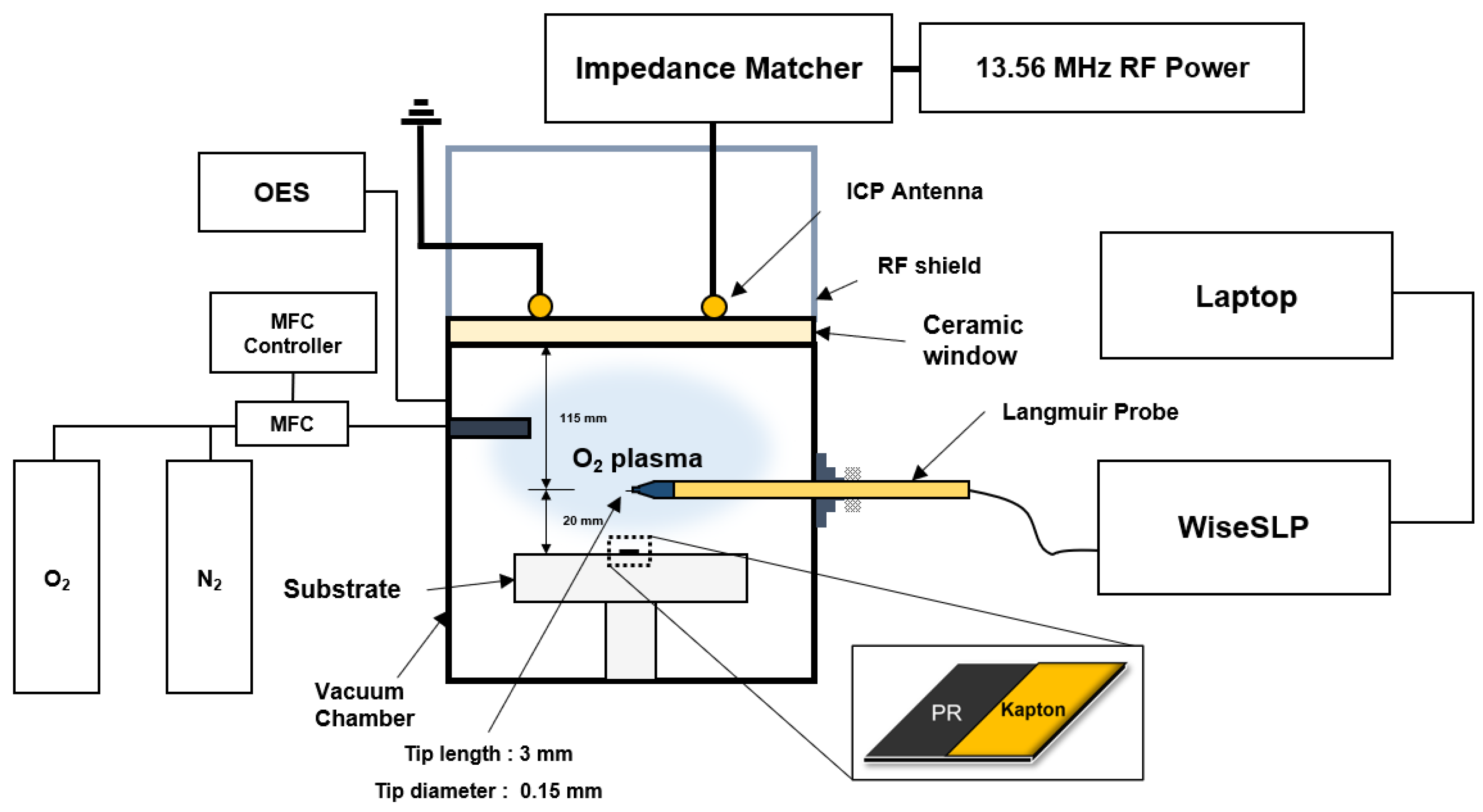
2. Experiment
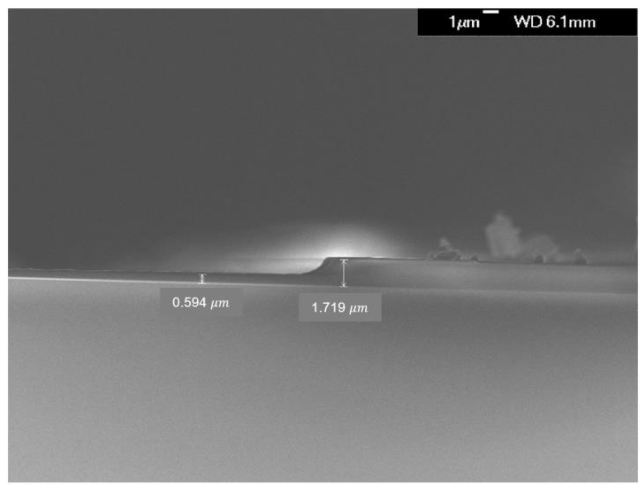
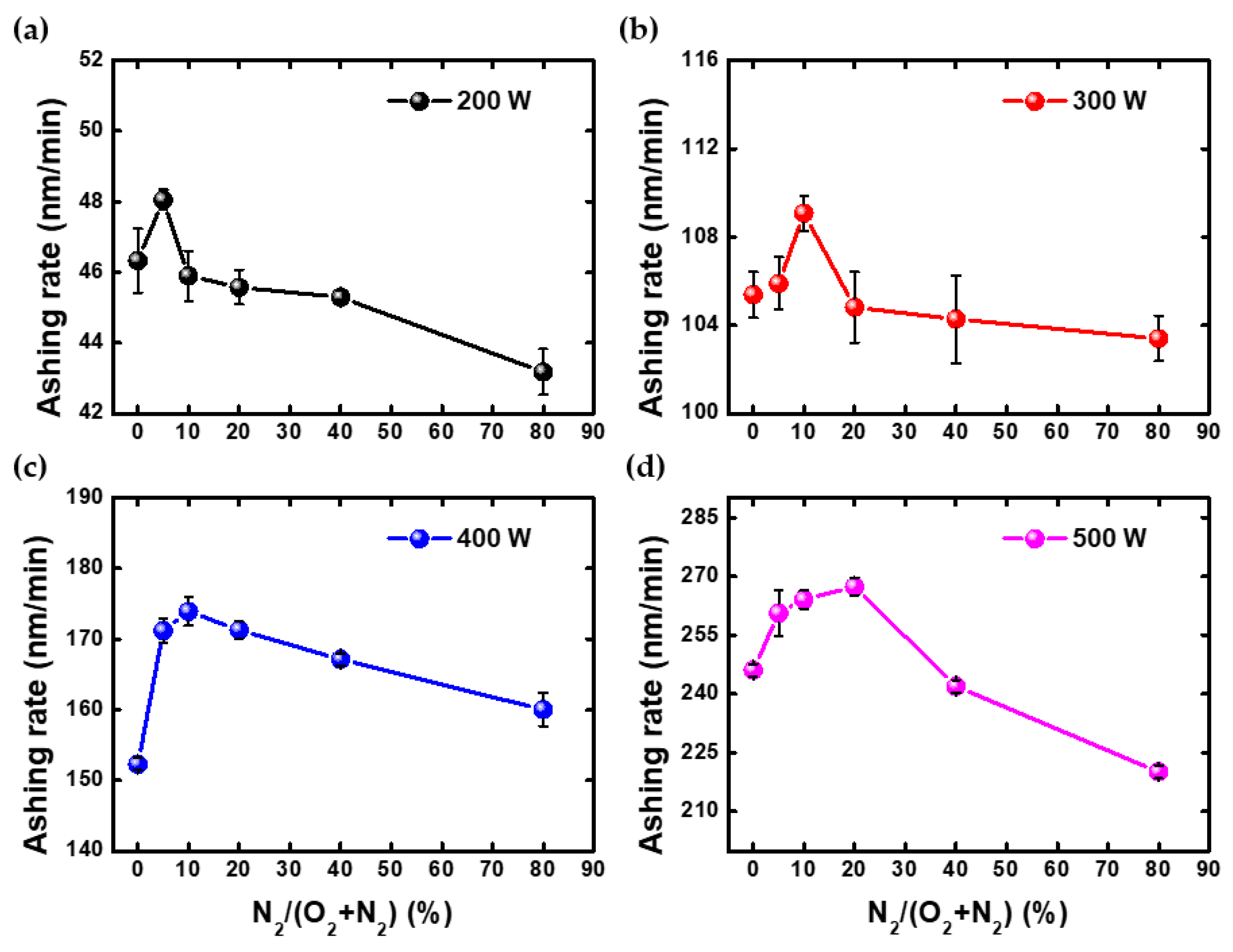
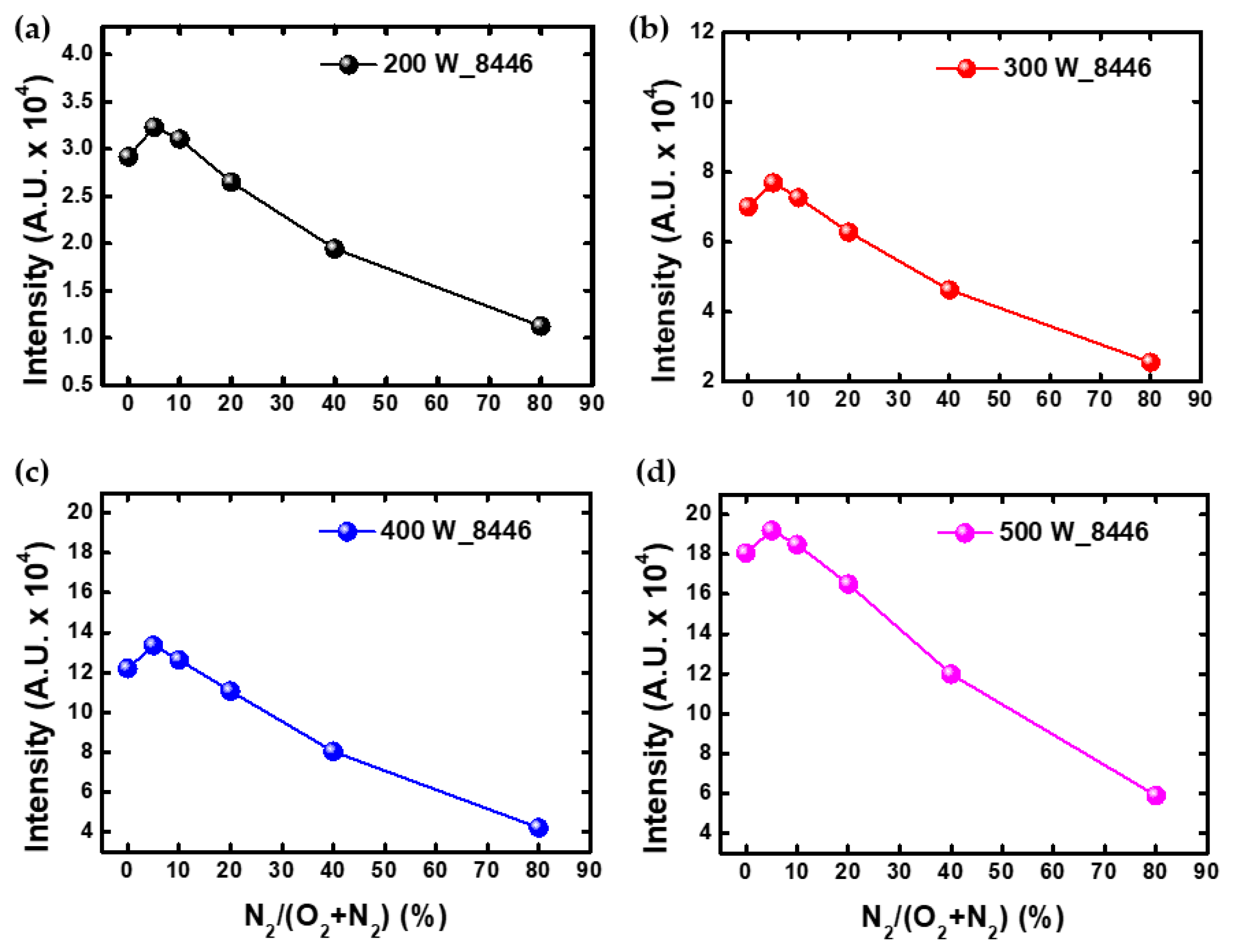
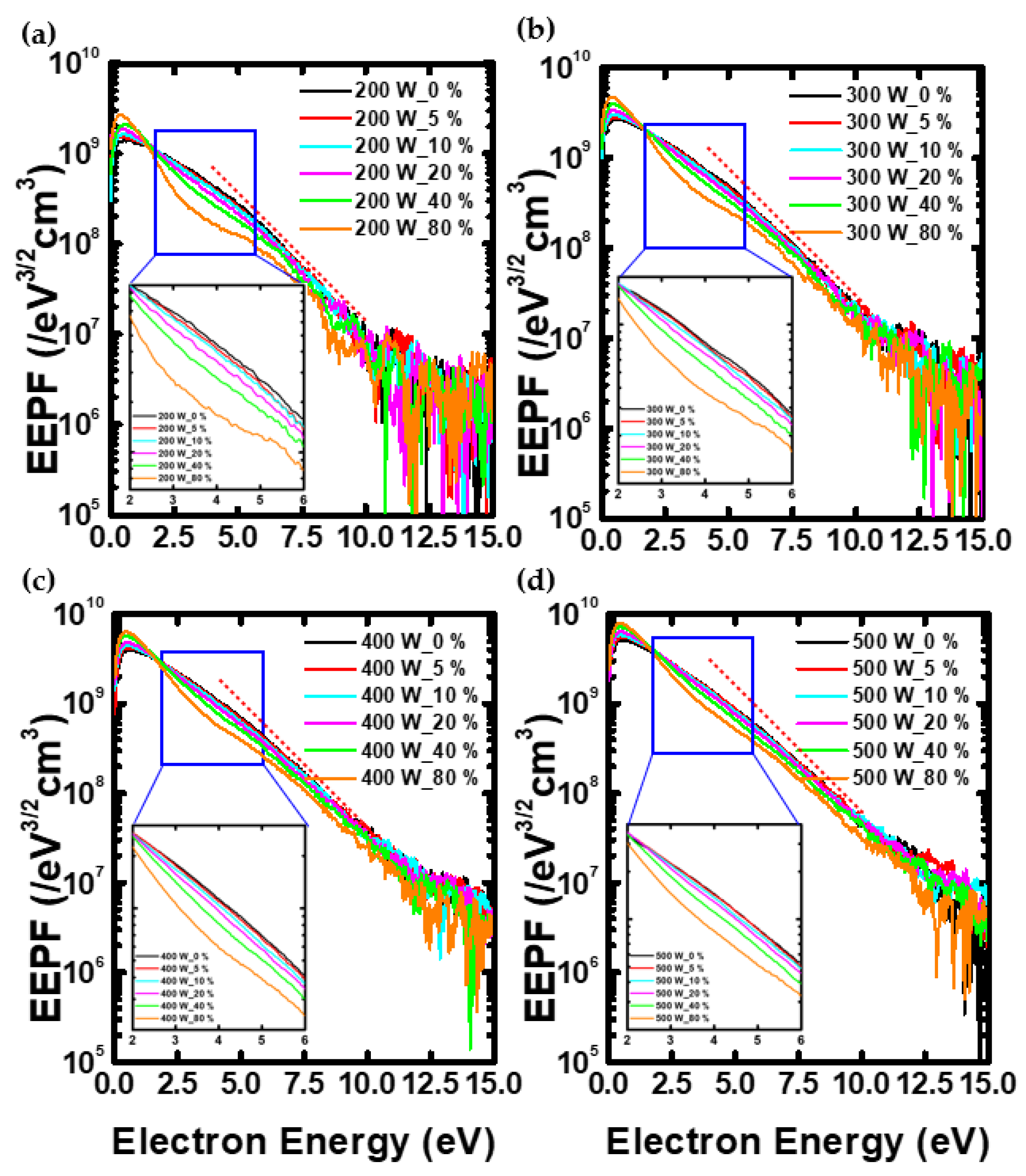
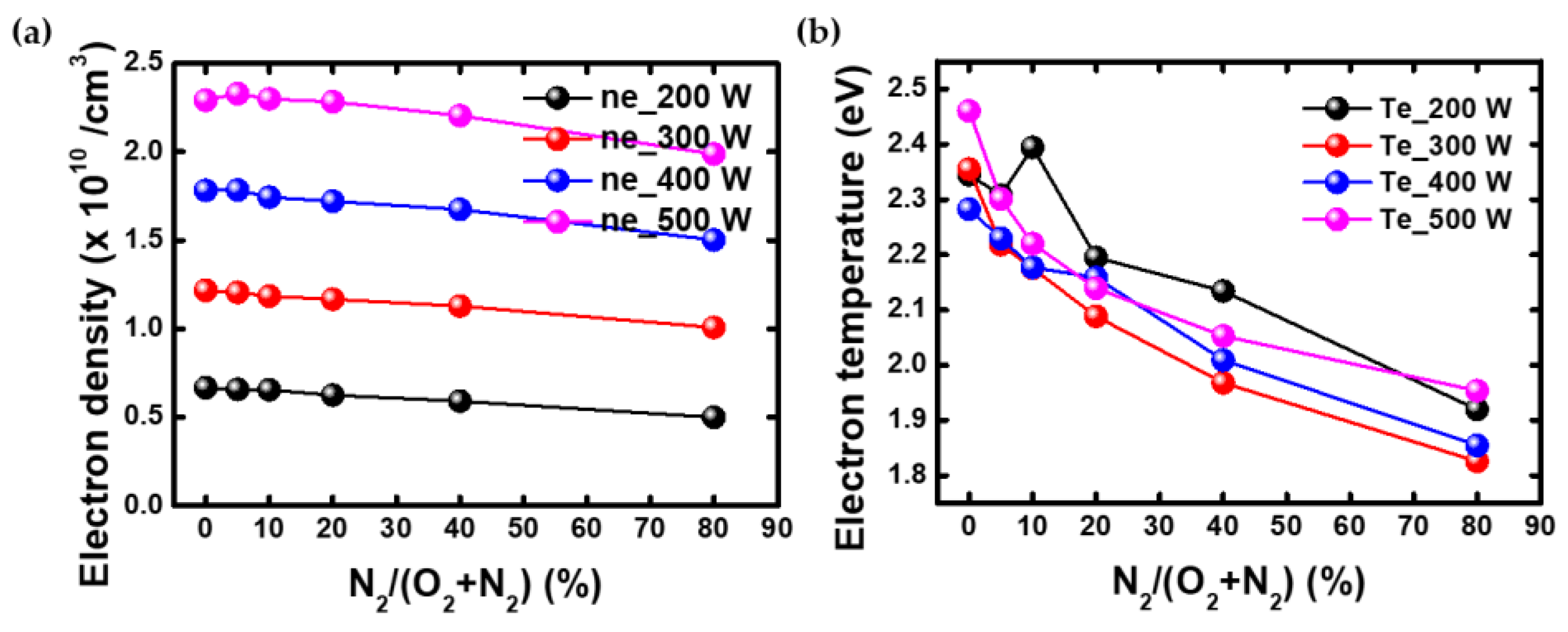
3. Results and Discussions
4. Conclusions
Author Contributions
Funding
Data Availability Statement
Conflicts of Interest
References
- Kim, M.; Moon, J.; Choi, J.; Park, S.; Lee, B.; Cho, M. Multiscale Simulation Approach on Sub-10 nm Extreme Ultraviolet Photoresist Patterning: Insights from Nanoscale Heterogeneity of Polymer. Macromolecules 2018, 51, 6922–6935. [Google Scholar] [CrossRef]
- Wachulak, P.W.; Capeluto, M.G.; Marconi, M.C.; Patel, D.; Menoni, C.S.; Rocca, J.J. Nanoscale Patterning in High Resolution HSQ Photoresist by Interferometric Lithography with Tabletop Extreme Ultraviolet Lasers. J. Vac. Sci. Technol. B Microelectron. Nanom. Struct. 2007, 25, 2094. [Google Scholar] [CrossRef] [Green Version]
- Fourkas, J.T. RAPID Lithography: New Photoresists Achieve Nanoscale Resolution. Opt. Photonics News 2011, 22, 24. [Google Scholar] [CrossRef]
- Stocker, M.P.; Li, L.; Gattass, R.R.; Fourkas, J.T. Multiphoton Photoresists Giving Nanoscale Resolution That Is Inversely Dependent on Exposure Time. Nat. Chem. 2011, 3, 223–227. [Google Scholar] [CrossRef]
- Claes, M.; Le, Q.; Kesters, E.; Lux, M.; Urionabarrenetxea, A.; Vereecke, G.; Mertens, P.; Carleer, R.; Adriaensens, P. All-Wet Strip Approaches for Post-Etch Photoresist Layers After Low-K Patterning. ECS Trans. 2007, 11, 177–187. [Google Scholar] [CrossRef]
- Wada, M.; Sano, K.; Snow, J.; Vos, R.; Leunissen, L.H.A.; Mertens, P.W.; Eitoku, A. All Wet Photoresist Strip by Solvent Aerosol Spray. Solid State Phenom. 2009, 145–146, 285–288. [Google Scholar] [CrossRef]
- Christenson, K.K.; Butterbaugh, J.W.; Wagener, T.J.; Lee, N.P.; Schwab, B.; Fussy, M.; Diedrick, J. All Wet Stripping of Implanted Photoresist. Solid State Phenom. 2008, 134, 109–112. [Google Scholar] [CrossRef]
- Dzioba, S.; Este, G.; Naguib, H.M. Decapsulation and Photoresist Stripping in Oxygen Microwave Plasmas. J. Electrochem. Soc. 1982, 129, 2537. [Google Scholar] [CrossRef]
- West, A.; Van Der Schans, M.; Xu, C.; Cooke, M.; Wagenaars, E. Fast, Downstream Removal of Photoresist Using Reactive Oxygen Species from the Effluent of an Atmospheric Pressure Plasma Jet. Plasma Sources Sci. Technol. 2016, 25, 02LT01. [Google Scholar] [CrossRef]
- Kikuchi, M.; Bersin, R. A Dry Process for Stripping As+ Ion-Implanted Photoresist. Jpn. J. Appl. Phys. 1992, 31, 2035–2040. [Google Scholar] [CrossRef]
- Wang, S.; Xu, X.; Zhao, L.; Ye, T. Photoresist Etching by Atmospheric Pressure Uniform-Glow Plasma. Jpn. J. Appl. Phys. Part 1 Regul. Pap. Short Notes Rev. Pap. 2007, 46, 5294–5296. [Google Scholar] [CrossRef]
- Hartney, M.A.; Hess, D.W.; Soane, D.S. Oxygen Plasma Etching for Resist Stripping and Multilayer Lithography Critical Review Oxygen Plasma Etching for Resist Stripping and Multilayer Lithography. J. Vac. Sci. Technol. B Microelectron. Process. Phenom. 1989, 7, 1–13. [Google Scholar] [CrossRef]
- Shim, K.H.; Yang, H.Y.; Kil, Y.H.; Yang, H.D.; Yang, J.H.; Hong, W.K.; Kang, S.; Jeong, T.S.; Kim, T.S. Nanoscale Dry Etching of Germanium by Using Inductively Coupled CF 4 Plasma. Electron. Mater. Lett. 2012, 8, 423–428. [Google Scholar] [CrossRef]
- Ishikawa, K.; Karahashi, K.; Ishijima, T.; Cho, S.I.; Elliott, S.; Hausmann, D.; Mocuta, D.; Wilson, A.; Kinoshita, K. Progress in Nanoscale Dry Processes for Fabrication of High-Aspect-Ratio Features: How Can We Control Critical Dimension Uniformity at the Bottom? Jpn. J. Appl. Phys. 2018, 57, 06JA01. [Google Scholar] [CrossRef]
- Huang, C.K.; Chen, Y.H.; Liang, Y.C.; Wu, T.B.; Chen, H.L.; Chao, W.C. Fabrication of Nanoscale PtOx/PZT/PtOx Capacitors by e-Beam Lithography and Plasma Etching with Photoresist Mask. Electrochem. Solid-State Lett. 2006, 9, 51–54. [Google Scholar] [CrossRef]
- Hua, X.; Engelmann, S.; Oehrlein, G.S.; Jiang, P.; Lazzeri, P.; Iacob, E.; Anderle, M. Studies of Plasma Surface Interactions during Short Time Plasma Etching of 193 and 248 Nm Photoresist Materials. J. Vac. Sci. Technol. B Microelectron. Nanom. Struct. 2006, 24, 1850. [Google Scholar] [CrossRef]
- Ponoth, S.; Agarwal, N.; Persans, P.; Plawsky, J. Silicon CMOS BEOL Compatible Optical Waveguide Micro-Mirrors. MRS Online Proc. Libr. 2002, 744, 475–480. [Google Scholar] [CrossRef]
- Susa, Y.; Ohtake, H.; Jianping, Z.; Chen, L.; Nozawa, T. Characterization of CO2 Plasma Ashing for Less Low-Dielectric-Constant Film Damage. J. Vac. Sci. Technol. A Vac. Surf. Film. 2015, 33, 061307. [Google Scholar] [CrossRef]
- Kuo, M.-S.; Pal, A.R.; Oehrlein, G.S.; Hua, X. Mechanistic Study of Ultralow K-Compatible Carbon Dioxide in Situ Photoresist Ashing Processes. II. Interaction with Preceding Fluorocarbon Plasma Ultralow k Etching Processes. J. Vac. Sci. Technol. B Nanotechnol. Microelectron. Mater. Process. Meas. Phenom. 2010, 28, 961–967. [Google Scholar] [CrossRef]
- Thedjoisworo, B.; Cheung, D.; Crist, V. Comparison of the Effects of Downstream H2- and O2-Based Plasmas on the Removal of Photoresist, Silicon, and Silicon Nitride. J. Vac. Sci. Technol. B Nanotechnol. Microelectron. Mater. Process. Meas. Phenom. 2013, 31, 021206. [Google Scholar] [CrossRef]
- Fujimura, S.; Shinagawa, K.; Nakamura, M.; Yano, H. Additive Nitrogen Effects on Oxygen Plasma Downstream Ashing. Jpn. J. Appl. Phys. 1990, 29, 2165–2170. [Google Scholar] [CrossRef]
- Brussaard, G.J.H.; Letourneur, K.G.Y.; Schaepkens, M.; van de Sanden, M.C.M.; Schram, D.C. Stripping of Photoresist Using a Remote Thermal Ar/O2 and Ar/N2/O2 Plasma. J. Vac. Sci. Technol. B Microelectron. Nanom. Struct. 2003, 21, 61. [Google Scholar] [CrossRef] [Green Version]
- Guerra, V.; Sá, P.A.; Loureiro, J. Role Played by the N2(A 3Σu+) Metastable in Stationary N2 and N2-O2 Discharges. J. Phys. D Appl. Phys. 2001, 34, 1745–1755. [Google Scholar] [CrossRef]
- Merlino, R.L. Understanding Langmuir Probe Current-Voltage Characteristics. Am. J. Phys. 2007, 75, 1078–1085. [Google Scholar] [CrossRef] [Green Version]
- Chen, F.F. Langmuir Probe Analysis for High Density Plasmas. Phys. Plasmas 2001, 8, 3029–3041. [Google Scholar] [CrossRef] [Green Version]
- Sudit, I.D.; Woods, R.C. A Study of the Accuracy of Various Langmuir Probe Theories. J. Appl. Phys. 1994, 76, 4488–4498. [Google Scholar] [CrossRef]
- Gottscho, R.A.; Donnelly, V.M. Optical Emission Actinometry and Spectral Line Shapes in Rf Glow Discharges. J. Appl. Phys. 1984, 56, 245–250. [Google Scholar] [CrossRef]
- Katsch, H.M.; Tewes, A.; Quandt, E.; Goehlich, A.; Kawetzki, T.; Döbele, H.F. Detection of Atomic Oxygen: Improvement of Actinometry and Comparison with Laser Spectroscopy. J. Appl. Phys. 2000, 88, 6232–6238. [Google Scholar] [CrossRef]
- Zhu, X.M.; Pu, Y.K. Optical Emission Spectroscopy in Low-Temperature Plasmas Containing Argon and Nitrogen: Determination of the Electron Temperature and Density by the Line-Ratio Method. J. Phys. D Appl. Phys. 2010, 43, 403001. [Google Scholar] [CrossRef]
- Devia, D.M.; Rodriguez-Restrepo, L.V.; Restrepo-Parra, E. Methods Employed in Optical Emission Spectroscopy Analysis: A Review. Ing. Y Cienc. 2015, 11, 239–267. [Google Scholar] [CrossRef]
- Chung, T.H.; Ra Kang, H.; Bae, M.K. Optical Emission Diagnostics with Electric Probe Measurements of Inductively Coupled Ar/O2/Ar-O2 Plasmas. Phys. Plasmas 2012, 19, 113502. [Google Scholar] [CrossRef]
- Woo, J.-C.; Ha, T.-K.; Kim, C.-I. The Dry Etching Characteristics of HfAlO3 Thin Films in CF4/Cl2/Ar Inductively Coupled Plasma. J. Electrochem. Soc. 2011, 159, D26–D30. [Google Scholar] [CrossRef]
- Karakas, E.; Donnelly, V.M.; Economou, D.J. Optical Emission Spectroscopy and Langmuir Probe Diagnostics of CH3F/O2 Inductively Coupled Plasmas. J. Appl. Phys. 2013, 113, 213301. [Google Scholar] [CrossRef]
- Li, H.; Zhou, Y.; Donnelly, V.M. Optical and Mass Spectrometric Measurements of Dissociation in Low Frequency, High Density, Remote Source O2/Ar and NF3/Ar Plasmas. J. Vac. Sci. Technol. A 2020, 38, 023011. [Google Scholar] [CrossRef]
- Cullen, P.J. Spectroscopic Characterization of a Radio-Frequency Argon Plasma Jet Discharge in Ambient Air. Prog. Theor. Exp. Phys. 2015, 2015, 1–17. [Google Scholar] [CrossRef] [Green Version]
- Lock, E.H.; Fernsler, R.F.; Slinker, S.; Walton, S.G. Experimental and Theoretical Estimation of Excited Species Generation in Pulsed Electron Beam—Generated Plasmas Produced in Pure Argon, Nitrogen, Oxygen, and Their Mixtures; Naval Research Laboratory: Washington, DC, USA, 2011. [Google Scholar]
- Conde, L. An Introduction to Langmuir Probe Diagnostics of Plasmas; ETSI Aeronáut Ngenieros Aeronáuticos Universidad Politécnica de Madrid: Madrid, Spain, 2011. [Google Scholar]
- Park, H.; You, S.J.; Choe, W. Correlation between Excitation Temperature and Electron Temperature with Two Groups of Electron Energy Distributions. Phys. Plasmas 2010, 17, 11–15. [Google Scholar] [CrossRef]
- Fuller, N.C.M.; Malyshev, M.V.; Donnelly, V.M.; Herman, I.P. Characterization of Transformer Coupled Oxygen Plasmas by Trace Rare Gases-Optical Emission Spectroscopy and Langmuir Probe Analysis. Plasma Sources Sci. Technol. 2000, 9, 116–127. [Google Scholar] [CrossRef]
- Lee, J.K.; Lee, H.C.; Chung, C.W. E-H Mode Transition in Inductively Coupled Plasma Using Ar, O2, N2, and Mixture Gas. Curr. Appl. Phys. 2011, 11, S149–S153. [Google Scholar] [CrossRef]
- Lee, H.C.; Lee, J.K.; Chung, C.W. Evolution of the Electron Energy Distribution and E-H Mode Transition in Inductively Coupled Nitrogen Plasma. Phys. Plasmas 2010, 17, 033506. [Google Scholar] [CrossRef]
- Phys, J.A. Floating Harmonics Method for Measuring Electron Temperature in Non-Maxwellian Plasmas. J. Appl. Phys. 2010, 107, 103312. [Google Scholar] [CrossRef]
- Germany, G.A.; Anderson, R.J.; Salamo, G.J. Electron Impact Excitation of the 3p(5P) State of Atomic Oxygen. J. Chem. Phys. 1988, 89, 1999–2002. [Google Scholar] [CrossRef]
- Bilik, N.; Anthony, R.; Merritt, B.A.; Aydil, E.S.; Kortshagen, U.R. Langmuir Probe Measurements of Electron Energy Probability Functions in Dusty Plasmas. J. Phys. D Appl. Phys. 2015, 48, 105204. [Google Scholar] [CrossRef]

Publisher’s Note: MDPI stays neutral with regard to jurisdictional claims in published maps and institutional affiliations. |
© 2022 by the authors. Licensee MDPI, Basel, Switzerland. This article is an open access article distributed under the terms and conditions of the Creative Commons Attribution (CC BY) license (https://creativecommons.org/licenses/by/4.0/).
Share and Cite
You, Y.-B.; Lee, Y.-S.; Kim, S.-J.; Cho, C.-H.; Seong, I.-H.; Jeong, W.-N.; Choi, M.-S.; You, S.-J. Influence of Additive N2 on O2 Plasma Ashing Process in Inductively Coupled Plasma. Nanomaterials 2022, 12, 3798. https://doi.org/10.3390/nano12213798
You Y-B, Lee Y-S, Kim S-J, Cho C-H, Seong I-H, Jeong W-N, Choi M-S, You S-J. Influence of Additive N2 on O2 Plasma Ashing Process in Inductively Coupled Plasma. Nanomaterials. 2022; 12(21):3798. https://doi.org/10.3390/nano12213798
Chicago/Turabian StyleYou, Ye-Bin, Young-Seok Lee, Si-Jun Kim, Chul-Hee Cho, In-Ho Seong, Won-Nyoung Jeong, Min-Su Choi, and Shin-Jae You. 2022. "Influence of Additive N2 on O2 Plasma Ashing Process in Inductively Coupled Plasma" Nanomaterials 12, no. 21: 3798. https://doi.org/10.3390/nano12213798
APA StyleYou, Y.-B., Lee, Y.-S., Kim, S.-J., Cho, C.-H., Seong, I.-H., Jeong, W.-N., Choi, M.-S., & You, S.-J. (2022). Influence of Additive N2 on O2 Plasma Ashing Process in Inductively Coupled Plasma. Nanomaterials, 12(21), 3798. https://doi.org/10.3390/nano12213798