
Raman Fingerprint of Interlayer Coupling in 2D TMDCs

1
Semiconductor Physics, Institute of Physics, Chemnitz University of Technology, 09111 Chemnitz, Germany
2
Center for Materials, Architectures, and Integration of Nanomembranes (MAIN), Chemnitz University of Technology, 09111 Chemnitz, Germany
*
Author to whom correspondence should be addressed.
Nanomaterials 2022, 12(22), 3949; https://doi.org/10.3390/nano12223949
Submission received: 20 October 2022
/
Revised: 3 November 2022
/
Accepted: 7 November 2022
/
Published: 9 November 2022
(This article belongs to the Special Issue Nanostructures for Advanced Photonic Devices)
Abstract
:Vertical stacking of two-dimensional (2D) homo- and heterostructures are intriguing research objects, as they are essential for fundamental studies and a key towards 2D device applications. It is paramount to understand the interlayer coupling in 2D materials and to find a fast yet precise characteristic signature. In this work, we report on a Raman fingerprint of interlayer coupling in 2D transition metal dichalcogenides (TMDCs). We observed that the out-of-plane vibrational mode is absent when two monolayers form a vertical stack yet remain uncoupled but emerges after strong coupling. Using systematic Raman, photoluminescence (PL), and atomic force microscopy (AFM) studies of WSe/WSe homo-bilayers and MoSe/WSe hetero-bilayers, we conclude that the vibrational mode is a distinct Raman fingerprint of interlayer coupling in 2D TMDCs. Our results propose an easy, fast, precise, and reliable measure to evaluate the interlayer coupling in 2D TMDCs.
1. Introduction
The weak van der Waals (vdW) interlayer coupling nature of 2D materials enables the possibility of vertical stacking, which leads to the formation of 2D homo- and heterostructures [1,2]. Novel physics phenomena emerge, and the mechanical, optical, electrical, and magnetic properties can be strongly tuned, when two or more layered materials are coupled to each other, or when the interlayer distance is tuned [3,4,5,6,7,8,9,10,11,12].
Vertical stacking of homo- or hetero-bilayer 2D materials forms moiré superlattices, which induce periodic modulations, potential distribution, phonon renormalization, and lattice reconstruction [13,14,15,16,17,18,19]. The unconventional superconductivity and correlated insulator behavior in magic-angle twisted bilayer graphene opened the door of moiré physics and attracted tremendous research attention to other 2D material systems [20,21]. Moreover, researchers observed interlayer excitons in various combination of TMDC heterostructures such as WSe/MoSe, MoS/WSe, and WSe/WS [22,23,24], as well as interlayer trions in WSe/MoSe/WSe heterostructures [25], which builds a promising platform for exploring many-body physics and new optoelectronic phenomena. The coupling of TMDC heterostructures forms pn junctions and can result in type-I, type-II, and type-III band alignment [26], which can significantly widen the application fields and enhance the device performance of transistors, memory devices, light-emitting diodes, photodetectors, and solar cells [27,28,29,30,31,32].
Proper interlayer coupling in 2D homo- and heterostructures is the key to preparing high-quality samples for fundamental studies and achieving high performance in devices. However, the 2D structures are often prepared by dry or wet transfer of mechanically exfoliated or CVD-grown 2D flakes, which always leave impurities consisting of atmospheric gases, water molecules, and hydrocarbons at the interfaces [33]. It is, therefore, paramount to find an easy, precise, and reliable characterization technique to evaluate the interlayer coupling in 2D devices. PL spectroscopy can be used to provide information about the interlayer coupling because of the direct-to-indirect bandgap transition from monolayer to multi-layer TMDCs, the formation of the interlayer excitons, charge transfer, and charge dissociation at the interface all lead to a strong quenching of the PL intensity [3,23,34,35]. However, charge transfer and dissociation can also happen at the interface between 2D materials and the substrates [34]. Moreover, the optical properties of 2D materials are strongly influenced by the substrate [36,37,38], which makes PL spectroscopy not an ideal tool for the characterization of interlayer coupling under certain circumstances, for instance, when 2D materials are supported by a metallic substrate. Raman spectroscopy, on the other hand, is a reliable and non-destructive technique to investigate lattice vibrations and phonon modes of materials. Low-frequency Raman spectroscopy has been intensively used because the interlayer shearing and breathing modes are highly sensitive to interlayer coupling [39,40,41,42,43,44,45]. However, the low-frequency Raman spectroscopy has the drawback of complicated and high-cost optical setup, relatively weak intensity, and disappearing of modes at certain twisting angles [16,41]. Moreover, the low-frequency Raman modes are so sensitive to interlayer coupling that they may also include signals originating from the coupling between 2D materials and hBN, which is commonly used for encapsulation, and thus makes data processing extremely challenging [16,46].
The high-frequency Raman features, on the other hand, are easy to access for almost any conventional Raman spectrometer and do not require extra complicated optical setups. It was reported that the frequency difference between the and vibrational modes for uncoupled artificially stacked bilayer MoS is similar to that of monolayer MoS rather than intrinsic bilayer MoS [45]. However, a distinct high-frequency Raman fingerprint of interlayer coupling in 2D TMDCs has not yet been revealed. In this work, we present a Raman spectroscopy study of interlayer coupling in WSe/WSe homo-bilayer and MoSe/WSe hetero-bilayer as prototypes of homo- and heterostructures. We observe that the out-of-plane vibrational mode is absent in the as-transferred homo- and hetero-bilayers but emerges after annealing. The out-of-plane mode is known to be Raman-active in pristine bilayer WSe from the perspective of symmetry [47]. The absence and re-emergence of the signal indicate a significant change in crystal structure and interlayer interaction. Since the samples are prepared on a dielectric substrate (300 nm SiO/Si) to exclude potential substrate effects, the PL measurements are considered as additional proof for the interlayer coupling. The AFM profiles suggest a significant height change after annealing, which also confirms the coupling. In general, our work demonstrates that the vibrational mode is a Raman fingerprint and an easy, fast, precise, and reliable measure to evaluate the interlayer coupling in 2D TMDCs, which is essential for fundamental studies and device applications.
2. Materials and Methods
2.1. Sample Preparation
Monolayer WSe and MoSe were mechanically exfoliated from bulk 2H-phase crystals (WSe from HQ Graphene, MoSe from 2D Semiconductors) onto polydimethylsiloxane (PDMS) by Nitto tape. The WSe homo-bilayer was prepared by a combination of a deterministic all-dry transfer technique and tear-and-stack method [19,48]. A large monolayer WSe flake was first exfoliated onto PDMS. The substrate was mounted on a rotation stage. Partial transfer of the monolayer WSe, rotation of the substrate by 60°, alignment of the flakes, and transfer again leads to an artificial 2H-phase bilayer WSe. The MoSe/WSe heterostructure was prepared by a deterministic all-dry transfer technique [48]. A detailed description of the sample preparation can be found in the Supplementary Information.
All samples are pre-characterized by PL and Raman spectroscopy on PDMS to identify the layer number. The samples were annealed in a nitrogen atmosphere at 150 °C for 2 h after the initial Raman, PL, and AFM measurements of the as-transferred homo- and hetero-bilayers.
2.2. Optical Spectroscopy
Raman and PL spectra were measured in ambient conditions with constant temperature and humidity using a Horiba XploRA Plus Raman Microscope equipped with a 100×, 0.9 NA objective, a spectrometer comprising 600 L/mm (for PL) and 2400 L/mm (for Raman) gratings, and an electron multiplying charge coupled device (EMCCD). A DPSS 532 nm continuous wave (CW) laser source was used to excite the samples with an excitation power of 100 µW measured under the objective. The Raman microscope is equipped with a Märzhäuser motorized stage with a 100 nm step size precision for Raman and PL mapping.
2.3. Atomic Force Microscope
We used an AIST-NT SmartSPM 1000 for AFM measurements. The AFM measurements were performed in ambient conditions with constant temperature and humidity. The NSG10 tip is commercially available with a typical tip radius of ∼6 nm.
3. Results and Discussion
3.1. WSe Homo-Bilayers
Figure 1a displays the three vibrational modes of WSe located in the spectral range of our interest. It is noteworthy that the irreducible representations (irreps) for the same vibrational mode may change in different layer numbers [47], but we refer to these phonon modes by their irreps in the bulk structures to be consistent. The (short for ) mode is an in-plane vibrational mode, where the W and Se atoms vibrate against each other. The and modes are out-of-plane vibrational modes. For the mode, the two Se atoms within the same layer vibrate against each other, while the W atom has no relative motion. For the mode, the Se and W atoms within the same layer vibrate against each other with a 180° phase difference to the vibration in the adjacent layers.
From the symmetry point of view, 2H-phase bulk, bilayer, and monolayer WSe belong to the , , and point groups, respectively [49]. The number of symmetry elements is reduced from 24 to 12 when the material is thinned from infinite to few layers. To be clear, though the numbers of symmetry elements are the same in both monolayer and bilayer WSe, the symmetry elements are actually different. There is one important element present in both bulk and monolayer but missing in bilayer WSe: a mirror plane in the W atom layer perpendicular to the c-axis [50]. The lack of this c-axis mirror plane in bilayer WSe makes the out-of-plane vibrational mode active [47]. In monolayer WSe, the existence of a c-axis mirror plane and the lack of an adjacent layer makes the mode inactive. The symmetry analysis interprets the Raman spectra in Figure 1b, where the mode at ∼309 cm is absent in monolayer WSe while it emerges in bilayer WSe. The most pronounced peak at ∼250 cm corresponds to the combination of and vibrational modes, almost degenerating at the same frequency [47,50,51,52]. The feature at ∼260 cm is a second-order peak caused by a double-resonance effect involving the longitudinal acoustic phonon at the M point in the Brillouin zone, which is usually assigned as 2LA(M) [52,53]. It is extremely sensitive to the resonance condition due to its double-resonance nature, which explains the different line shapes between monolayer and bilayer WSe [53,54].
We suggest that the vibrational mode should be a good measure for the interlayer coupling in 2D TMDCs because of the unique property mentioned above. To confirm our hypothesis, we prepared an artificial bilayer WSe with a 60° relative twisting angle (shown in Figure 2a) to simulate the situation of the intrinsic bilayer and measured Raman, PL, and AFM before and after the coupling (annealing). It is well known that the interlayer coupling of as-transferred homo- and heterostructures is usually poor [23,33]. Annealing is a practical strategy to improve the interlayer coupling due to the self-cleansing mechanism in vdW heterostructures. The elastic potential energy-induced affinities are higher among the adjacent layers than that between 2D materials and the impurities. The impurities are physically mobile and, therefore, can be driven by the affinity to migrate along the interfaces and finally form isolated bubbles [2,55,56].
Indeed, as shown in the Raman intensity map and spectra in Figure 2b–d, the mode does not exist in monolayer WSe and bilayer WSe before annealing. However, a clear peak emerges after annealing. The shape of the monolayer flake in the Raman intensity maps in Figure 2b,c originates from the slight change in the background signal. Since a dielectric substrate is used for the sample, the influence of the substrate is negligible in this case. Therefore, PL provides strong additional evidence for the interlayer coupling. As shown in the PL intensity map before annealing in Figure 2e, the PL intensity is extremely high due to the direct bandgap nature of monolayer WSe, which leads to high radiative recombination efficiency [3,57]. The uncoupled bilayer emits almost twice the intensity as the monolayer part. However, a strong PL quenching is observed on the bilayer part after annealing, as demonstrated in Figure 2f. The strong decrease in PL intensity is caused by the change from direct bandgap in monolayer to indirect bandgap semiconductor in bilayer [3]. An extra emission feature corresponding to the indirect bandgap transition is also observed in Figure 2g. The PL measurements are in excellent agreement with the Raman measurements confirming that the as-transferred bilayer is not coupled, while becoming strongly coupled after annealing. Note that the bilayer area rolled up a bit after annealing along the wrinkle, which causes a slight change in the sample area before and after annealing (as shown in Figure S3 in the Supplementary Information). The comparison of optical microscope images before and after annealing can be found in the Supplementary Materials. All spectra displayed here are taken from the non-rolled-up area.
In addition to the optical spectroscopy measurements, we also investigated the topography of the samples before and after annealing by means of an atomic force microscope. A clear change in AFM topography is observed. First, the bubbles on the bilayer area in Figure 3a diffuse along the interface and form the big bubbles in Figure 3b. This phenomenon confirms the self-cleaning mechanism in vdW heterostructures. More interestingly, the height profile in Figure 3d suggests that the distance between the top Se atom layer of each individual monolayer decreases from 4.0 nm to 0.7 nm, which agrees with the reported thickness of monolayer WSe [58]. The PL and AFM results conclusively confirm that the as-transferred bilayer is not coupled and behaves like two independent monolayers, while becoming tightly coupled after annealing. Combining the Raman, PL, and AFM measurements, it is shown that the mode is a reliable measure for the interlayer coupling in homo-bilayers.
3.2. MoSe/WSe Hetero-Bilayers
We demonstrated that the vibrational mode can be considered as a Raman fingerprint to evaluate the interlayer coupling in WSe/WSe homo-bilayers. Furthermore, we investigated the interlayer coupling in TMDC heterostructures using MoSe/WSe hetero-bilayer as a prototype.
Figure 4a displays the Raman spectra of monolayer and bilayer MoSe. MoSe has three Raman active modes in the spectral range of our interest, which correspond to the out-of-plane mode, in-plane mode, and out-of-plane mode located at ∼241 cm, ∼287 cm, and ∼353 cm, respectively. Similar to WSe, the vibrational mode is inactive in bulk and monolayer but becomes active in the bilayer [51].
Figure 4b shows the Raman spectra of monolayer WSe, MoSe, and MoSe/WSe heterostructure before and after annealing. The Raman spectra of MoSe/WSe heterostructure before annealing is simply a superposition of the Raman spectra of monolayer MoSe and WSe. Interestingly, both individual modes of WSe and MoSe emerge after the coupling (annealing). As the key point for the mode to be active is the existence of an adjacent layer and the 180° vibrational phase difference, we propose that the similar structure of TDMCs makes the detection of the mode a fingerprint for bilayer coupling applicable widely for various TMDC combinations. It was reported that the combination of MoSe and WSe forms interlayer excitons [22], at which point the PL intensity is significantly quenched due to the interlayer charge transfer. Indeed, we observed a ∼25 times PL quenching and an interlayer exciton emission feature at ∼1.35 eV on MoSe/WSe heterostructure after annealing, as shown in Figure 4c, which confirms the proper coupling after annealing. We, therefore, propose that the vibrational mode also serves as a Raman fingerprint for interlayer coupling in TMDC heterostructures.
4. Conclusions
In summary, taking WSe/WSe homo-bilayer and MoSe/WSe hetero-bilayer as prototypes, we investigated the interlayer coupling in 2D TDMCs. Using systematic Raman, PL, and AFM, we conclude that the out-of-plane vibrational mode is the Raman fingerprint of interlayer coupling. The mode is absent in an uncoupled vertical stack, but emerges after the coupling. Our work demonstrates an easy, fast, precise, and reliable measure to evaluate interlayer coupling in 2D TMDCs, which is essential for fundamental studies and device applications.
Supplementary Materials
The following supporting information can be downloaded at: https://www.mdpi.com/article/10.3390/nano12223949/s1, Figure S1: Sample preparation of WSe/WSe homo-bilayer; Figure S2: Sample preparation of MoSe/WSe hetero-bilayer; Figure S3: WSe/WSe homo-bilayer before and after annealing; Figure S4: Raman and PL map of MoSe/WSe hetero-bilayer.
Author Contributions
Conceptualization, Y.P. and D.R.T.Z.; methodology, Y.P. and D.R.T.Z.; validation, Y.P. and D.R.T.Z.; formal analysis, Y.P.; investigation, Y.P.; resources, D.R.T.Z.; data curation, Y.P.; writing—original draft preparation, Y.P.; writing—review and editing, Y.P. and D.R.T.Z.; visualization, Y.P.; supervision, D.R.T.Z.; project administration, D.R.T.Z.; funding acquisition, D.R.T.Z. All authors have read and agreed to the published version of the manuscript.
Funding
This research was funded by Deutsche Forschungsgemeinschaft (DFG) grant number ZA-146/47-1.
Data Availability Statement
The data presented in this study are available on request from the corresponding author.
Acknowledgments
The authors thank Shutong Li for the discussion and symmetry analysis.
Conflicts of Interest
The authors declare no conflict of interest.
References
- Geim, A.K.; Grigorieva, I.V. Van der Waals heterostructures. Nature 2013, 499, 419–425. [Google Scholar] [CrossRef] [PubMed] [Green Version]
- Novoselov, K.S.; Mishchenko, A.; Carvalho, A.; Castro Neto, A.H. 2D materials and van der Waals heterostructures. Science 2016, 353, aac9439. [Google Scholar] [CrossRef] [PubMed] [Green Version]
- Splendiani, A.; Sun, L.; Zhang, Y.; Li, T.; Kim, J.; Chim, C.Y.; Galli, G.; Wang, F. Emerging photoluminescence in monolayer MoS2. Nano Lett. 2010, 10, 1271–1275. [Google Scholar] [CrossRef]
- Androulidakis, C.; Zhang, K.; Robertson, M.; Tawfick, S. Tailoring the mechanical properties of 2D materials and heterostructures. 2D Mater. 2018, 5, 032005. [Google Scholar] [CrossRef]
- Yuan, L.; Chung, T.F.; Kuc, A.; Wan, Y.; Xu, Y.; Chen, Y.P.; Heine, T.; Huang, L. Photocarrier generation from interlayer charge-transfer transitions in WS2-graphene heterostructures. Sci. Adv. 2018, 4, e1700324. [Google Scholar] [CrossRef] [Green Version]
- Zhou, J.; Kong, X.; Sekhar, M.C.; Lin, J.; Le Goualher, F.; Xu, R.; Wang, X.; Chen, Y.; Zhou, Y.; Zhu, C.; et al. Epitaxial synthesis of monolayer PtSe2 single crystal on MoSe2 with strong interlayer coupling. ACS Nano 2019, 13, 10929–10938. [Google Scholar] [CrossRef]
- Peng, B.; Yu, G.; Liu, X.; Liu, B.; Liang, X.; Bi, L.; Deng, L.; Sum, T.C.; Loh, K.P. Ultrafast charge transfer in MoS2/WSe2 p–n Heterojunction. 2D Mater. 2016, 3, 025020. [Google Scholar] [CrossRef]
- Ceballos, F.; Ju, M.G.; Lane, S.D.; Zeng, X.C.; Zhao, H. Highly efficient and anomalous charge transfer in van der Waals trilayer semiconductors. Nano Lett. 2017, 17, 1623–1628. [Google Scholar] [CrossRef]
- Dai, S.; Ma, Q.; Liu, M.; Andersen, T.; Fei, Z.; Goldflam, M.; Wagner, M.; Watanabe, K.; Taniguchi, T.; Thiemens, M.; et al. Graphene on hexagonal boron nitride as a tunable hyperbolic metamaterial. Nat. Nanotechnol. 2015, 10, 682–686. [Google Scholar] [CrossRef]
- Li, Y.; Yang, B.; Xu, S.; Huang, B.; Duan, W. Emergent Phenomena in Magnetic Two-Dimensional Materials and van der Waals Heterostructures. ACS Appl. Electron. Mater. 2022, 4, 3278–3302. [Google Scholar] [CrossRef]
- Kistanov, A.A.; Cai, Y.; Zhou, K.; Dmitriev, S.V.; Zhang, Y.W. Effects of graphene/BN encapsulation, surface functionalization and molecular adsorption on the electronic properties of layered InSe: A first-principles study. Phys. Chem. Chem. Phys. 2018, 20, 12939–12947. [Google Scholar] [CrossRef] [PubMed] [Green Version]
- Chernozatonskii, L.A.; Katin, K.P.; Kochaev, A.I.; Maslov, M.M. Moiré and non-twisted sp3-hybridized structures based on hexagonal boron nitride bilayers: Ab initio insight into infrared and Raman spectra, bands structures and mechanical properties. Appl. Surf. Sci. 2022, 606, 154909. [Google Scholar] [CrossRef]
- Tran, K.; Moody, G.; Wu, F.; Lu, X.; Choi, J.; Kim, K.; Rai, A.; Sanchez, D.A.; Quan, J.; Singh, A.; et al. Evidence for moiré excitons in van der Waals heterostructures. Nature 2019, 567, 71–75. [Google Scholar] [CrossRef] [PubMed] [Green Version]
- Zhang, C.; Chuu, C.P.; Ren, X.; Li, M.Y.; Li, L.J.; Jin, C.; Chou, M.Y.; Shih, C.K. Interlayer couplings, Moiré patterns, and 2D electronic superlattices in MoS2/WSe2 hetero-bilayers. Sci. Adv. 2017, 3, e1601459. [Google Scholar] [CrossRef] [Green Version]
- Li, H.; Li, S.; Naik, M.H.; Xie, J.; Li, X.; Wang, J.; Regan, E.; Wang, D.; Zhao, W.; Zhao, S.; et al. Imaging moiré flat bands in three-dimensional reconstructed WSe2/WS2 superlattices. Nat. Mater. 2021, 20, 945–950. [Google Scholar] [CrossRef]
- Quan, J.; Linhart, L.; Lin, M.L.; Lee, D.; Zhu, J.; Wang, C.Y.; Hsu, W.T.; Choi, J.; Embley, J.; Young, C.; et al. Phonon renormalization in reconstructed MoS2 moiré superlattices. Nat. Mater. 2021, 20, 1100–1105. [Google Scholar] [CrossRef]
- Gadelha, A.C.; Ohlberg, D.A.; Rabelo, C.; Neto, E.G.; Vasconcelos, T.L.; Campos, J.L.; Lemos, J.S.; Ornelas, V.; Miranda, D.; Nadas, R.; et al. Localization of lattice dynamics in low-angle twisted bilayer graphene. Nature 2021, 590, 405–409. [Google Scholar] [CrossRef]
- Yu, J.; Giridharagopal, R.; Li, Y.; Xie, K.; Li, J.; Cao, T.; Xu, X.; Ginger, D.S. Imaging graphene moiré superlattices via scanning Kelvin probe microscopy. Nano Lett. 2021, 21, 3280–3286. [Google Scholar] [CrossRef]
- Pan, Y.; Li, S.; Rahaman, M.; Milekhin, I.; Zahn, D.R.T. Signature of lattice dynamics in twisted 2D homo/hetero-bilayers. 2D Mater. 2022, 9, 045018. [Google Scholar] [CrossRef]
- Cao, Y.; Fatemi, V.; Fang, S.; Watanabe, K.; Taniguchi, T.; Kaxiras, E.; Jarillo-Herrero, P. Unconventional superconductivity in magic-angle graphene superlattices. Nature 2018, 556, 43–50. [Google Scholar] [CrossRef]
- Cao, Y.; Fatemi, V.; Demir, A.; Fang, S.; Tomarken, S.L.; Luo, J.Y.; Sanchez-Yamagishi, J.D.; Watanabe, K.; Taniguchi, T.; Kaxiras, E.; et al. Correlated insulator behaviour at half-filling in magic-angle graphene superlattices. Nature 2018, 556, 80–84. [Google Scholar] [CrossRef] [PubMed] [Green Version]
- Rivera, P.; Schaibley, J.R.; Jones, A.M.; Ross, J.S.; Wu, S.; Aivazian, G.; Klement, P.; Seyler, K.; Clark, G.; Ghimire, N.J.; et al. Observation of long-lived interlayer excitons in monolayer MoSe2–WSe2 heterostructures. Nat. Commun. 2015, 6, 1–6. [Google Scholar] [CrossRef] [Green Version]
- Kunstmann, J.; Mooshammer, F.; Nagler, P.; Chaves, A.; Stein, F.; Paradiso, N.; Plechinger, G.; Strunk, C.; Schüller, C.; Seifert, G.; et al. Momentum-space indirect interlayer excitons in transition-metal dichalcogenide van der Waals heterostructures. Nat. Phys. 2018, 14, 801–805. [Google Scholar] [CrossRef] [Green Version]
- Okada, M.; Kutana, A.; Kureishi, Y.; Kobayashi, Y.; Saito, Y.; Saito, T.; Watanabe, K.; Taniguchi, T.; Gupta, S.; Miyata, Y.; et al. Direct and indirect interlayer excitons in a van der Waals heterostructure of hBN/WS2/MoS2/hBN. ACS Nano 2018, 12, 2498–2505. [Google Scholar] [CrossRef] [PubMed]
- Choi, C.; Huang, J.; Cheng, H.C.; Kim, H.; Vinod, A.K.; Bae, S.H.; Özçelik, V.O.; Grassi, R.; Chae, J.; Huang, S.W.; et al. Enhanced interlayer neutral excitons and trions in trilayer van der Waals heterostructures. Npj 2D Mater. Appl. 2018, 2, 1–9. [Google Scholar] [CrossRef] [Green Version]
- Chaves, A.; Azadani, J.G.; Alsalman, H.; Da Costa, D.; Frisenda, R.; Chaves, A.; Song, S.H.; Kim, Y.D.; He, D.; Zhou, J.; et al. Bandgap engineering of two-dimensional semiconductor materials. Npj 2D Mater. Appl. 2020, 4, 1–21. [Google Scholar] [CrossRef]
- Iannaccone, G.; Bonaccorso, F.; Colombo, L.; Fiori, G. Quantum engineering of transistors based on 2D materials heterostructures. Nat. Nanotechnol. 2018, 13, 183–191. [Google Scholar] [CrossRef]
- Guo, J.; Wang, L.; Yu, Y.; Wang, P.; Huang, Y.; Duan, X. SnSe/MoS2 van der Waals Heterostructure Junction Field-Effect Transistors with Nearly Ideal Subthreshold Slope. Adv. Mater. 2019, 31, 1902962. [Google Scholar] [CrossRef]
- Liu, C.; Yan, X.; Song, X.; Ding, S.; Zhang, D.W.; Zhou, P. A semi-floating gate memory based on van der Waals heterostructures for quasi-non-volatile applications. Nat. Nanotechnol. 2018, 13, 404–410. [Google Scholar] [CrossRef]
- Nikam, R.D.; Sonawane, P.A.; Sankar, R.; Chen, Y.T. Epitaxial growth of vertically stacked p-MoS2/n-MoS2 heterostructures by chemical vapor deposition for light emitting devices. Nano Energy 2017, 32, 454–462. [Google Scholar] [CrossRef]
- Xue, H.; Dai, Y.; Kim, W.; Wang, Y.; Bai, X.; Qi, M.; Halonen, K.; Lipsanen, H.; Sun, Z. High photoresponsivity and broadband photodetection with a band-engineered WSe2/SnSe2 heterostructure. Nanoscale 2019, 11, 3240–3247. [Google Scholar] [CrossRef] [PubMed] [Green Version]
- Furchi, M.M.; Höller, F.; Dobusch, L.; Polyushkin, D.K.; Schuler, S.; Mueller, T. Device physics of van der Waals heterojunction solar cells. Npj 2D Mater. Appl. 2018, 2, 1–7. [Google Scholar] [CrossRef] [Green Version]
- Fan, S.; Vu, Q.A.; Tran, M.D.; Adhikari, S.; Lee, Y.H. Transfer assembly for two-dimensional van der Waals heterostructures. 2D Mater. 2020, 7, 022005. [Google Scholar] [CrossRef]
- Rojas-Lopez, R.R.; Brant, J.C.; Ramos, M.S.; Castro, T.H.; Guimarães, M.H.; Neves, B.R.; Guimarães, P.S. Photoluminescence and charge transfer in the prototypical 2D/3D semiconductor heterostructure MoS2/GaAs. Appl. Phys. Lett. 2021, 119, 233101. [Google Scholar] [CrossRef]
- Meng, Y.; Wang, T.; Jin, C.; Li, Z.; Miao, S.; Lian, Z.; Taniguchi, T.; Watanabe, K.; Song, F.; Shi, S.F. Electrical switching between exciton dissociation to exciton funneling in MoSe2/WS2 heterostructure. Nat. Commun. 2020, 11, 1–6. [Google Scholar] [CrossRef]
- Lippert, S.; Schneider, L.M.; Renaud, D.; Kang, K.N.; Ajayi, O.; Kuhnert, J.; Halbich, M.U.; Abdulmunem, O.M.; Lin, X.; Hassoon, K.; et al. Influence of the substrate material on the optical properties of tungsten diselenide monolayers. 2D Mater. 2017, 4, 025045. [Google Scholar] [CrossRef]
- Schneider, L.; Lippert, S.; Kuhnert, J.; Renaud, D.; Kang, K.; Ajayi, O.; Halbich, M.U.; Abdulmunem, O.; Lin, X.; Hassoon, K.; et al. The impact of the substrate material on the optical properties of 2D WSe2 monolayers. Semiconductors 2018, 52, 565–571. [Google Scholar] [CrossRef]
- Rahaman, M.; Selyshchev, O.; Pan, Y.; Schwartz, R.; Milekhin, I.; Sharma, A.; Salvan, G.; Gemming, S.; Korn, T.; Zahn, D.R. Observation of Room-Temperature Dark Exciton Emission in Nanopatch-Decorated Monolayer WSe2 on Metal Substrate. Adv. Opt. Mater. 2021, 9, 2101801. [Google Scholar] [CrossRef]
- Saito, R.; Tatsumi, Y.; Huang, S.; Ling, X.; Dresselhaus, M. Raman spectroscopy of transition metal dichalcogenides. J. Physics Condens. Matter 2016, 28, 353002. [Google Scholar] [CrossRef]
- Huang, S.; Liang, L.; Ling, X.; Puretzky, A.A.; Geohegan, D.B.; Sumpter, B.G.; Kong, J.; Meunier, V.; Dresselhaus, M.S. Low-frequency interlayer Raman modes to probe interface of twisted bilayer MoS2. Nano Lett. 2016, 16, 1435–1444. [Google Scholar] [CrossRef]
- Parzefall, P.; Holler, J.; Scheuck, M.; Beer, A.; Lin, K.Q.; Peng, B.; Monserrat, B.; Nagler, P.; Kempf, M.; Korn, T.; et al. Moiré phonons in twisted MoSe2–WSe2 heterobilayers and their correlation with interlayer excitons. 2D Mater. 2021, 8, 035030. [Google Scholar] [CrossRef]
- Lin, K.Q.; Holler, J.; Bauer, J.M.; Parzefall, P.; Scheuck, M.; Peng, B.; Korn, T.; Bange, S.; Lupton, J.M.; Schüller, C. Large-scale mapping of moiré superlattices by hyperspectral Raman imaging. Adv. Mater. 2021, 33, 2008333. [Google Scholar] [CrossRef] [PubMed]
- Zhang, J.; Wang, J.; Chen, P.; Sun, Y.; Wu, S.; Jia, Z.; Lu, X.; Yu, H.; Chen, W.; Zhu, J.; et al. Observation of strong interlayer coupling in MoS2/WS2 heterostructures. Adv. Mater. 2016, 28, 1950–1956. [Google Scholar] [CrossRef] [PubMed]
- Xia, J.; Yan, J.; Wang, Z.; He, Y.; Gong, Y.; Chen, W.; Sum, T.C.; Liu, Z.; Ajayan, P.M.; Shen, Z. Strong coupling and pressure engineering in WSe2–MoSe2 heterobilayers. Nat. Phys. 2021, 17, 92–98. [Google Scholar] [CrossRef]
- Sarkar, S.; Pradeepa, H.; Nayak, G.; Marty, L.; Renard, J.; Coraux, J.; Bendiab, N.; Bouchiat, V.; Basu, J.K.; Bid, A. Evolution of inter-layer coupling in artificially stacked bilayer MoS2. Nanoscale Adv. 2019, 1, 4398–4405. [Google Scholar] [CrossRef] [Green Version]
- Lin, M.L.; Zhou, Y.; Wu, J.B.; Cong, X.; Liu, X.L.; Zhang, J.; Li, H.; Yao, W.; Tan, P.H. Cross-dimensional electron-phonon coupling in van der Waals heterostructures. Nat. Commun. 2019, 10, 1–9. [Google Scholar] [CrossRef] [Green Version]
- Luo, X.; Zhao, Y.; Zhang, J.; Toh, M.; Kloc, C.; Xiong, Q.; Quek, S.Y. Effects of lower symmetry and dimensionality on Raman spectra in two-dimensional WSe2. Phys. Rev. B 2013, 88, 195313. [Google Scholar] [CrossRef]
- Castellanos-Gomez, A.; Buscema, M.; Molenaar, R.; Singh, V.; Janssen, L.; Van Der Zant, H.S.; Steele, G.A. Deterministic transfer of two-dimensional materials by all-dry viscoelastic stamping. 2D Mater. 2014, 1, 011002. [Google Scholar] [CrossRef]
- Ribeiro-Soares, J.; Almeida, R.; Barros, E.B.; Araujo, P.T.; Dresselhaus, M.S.; Cançado, L.G.; Jorio, A. Group theory analysis of phonons in two-dimensional transition metal dichalcogenides. Phys. Rev. B 2014, 90, 115438. [Google Scholar] [CrossRef] [Green Version]
- Zhao, W.; Ghorannevis, Z.; Amara, K.K.; Pang, J.R.; Toh, M.; Zhang, X.; Kloc, C.; Tan, P.H.; Eda, G. Lattice dynamics in mono-and few-layer sheets of WS2 and WSe2. Nanoscale 2013, 5, 9677–9683. [Google Scholar] [CrossRef]
- Tonndorf, P.; Schmidt, R.; Böttger, P.; Zhang, X.; Börner, J.; Liebig, A.; Albrecht, M.; Kloc, C.; Gordan, O.; Zahn, D.R.; et al. Photoluminescence emission and Raman response of monolayer MoS2, MoSe2, and WSe2. Opt. Express 2013, 21, 4908–4916. [Google Scholar] [CrossRef] [PubMed]
- Terrones, H.; Corro, E.D.; Feng, S.; Poumirol, J.; Rhodes, D.; Smirnov, D.; Pradhan, N.; Lin, Z.; Nguyen, M.; Elías, A.; et al. New first order Raman-active modes in few layered transition metal dichalcogenides. Sci. Rep. 2014, 4, 4215. [Google Scholar] [CrossRef] [PubMed] [Green Version]
- Del Corro, E.; Terrones, H.; Elias, A.; Fantini, C.; Feng, S.; Nguyen, M.A.; Mallouk, T.E.; Terrones, M.; Pimenta, M.A. Excited excitonic states in 1L, 2L, 3L, and bulk WSe2 observed by resonant Raman spectroscopy. Acs Nano 2014, 8, 9629–9635. [Google Scholar] [CrossRef] [PubMed]
- Shi, W.; Lin, M.L.; Tan, Q.H.; Qiao, X.F.; Zhang, J.; Tan, P.H. Raman and photoluminescence spectra of two-dimensional nanocrystallites of monolayer WS2 and WSe2. 2D Mater. 2016, 3, 025016. [Google Scholar] [CrossRef] [Green Version]
- Tongay, S.; Fan, W.; Kang, J.; Park, J.; Koldemir, U.; Suh, J.; Narang, D.S.; Liu, K.; Ji, J.; Li, J.; et al. Tuning interlayer coupling in large-area heterostructures with CVD-grown MoS2 and WS2 monolayers. Nano Lett. 2014, 14, 3185–3190. [Google Scholar] [CrossRef]
- Kretinin, A.; Cao, Y.; Tu, J.; Yu, G.; Jalil, R.; Novoselov, K.; Haigh, S.; Gholinia, A.; Mishchenko, A.; Lozada, M.; et al. Electronic properties of graphene encapsulated with different two-dimensional atomic crystals. Nano Lett. 2014, 14, 3270–3276. [Google Scholar] [CrossRef] [Green Version]
- Li, Y.; Li, X.; Yu, T.; Yang, G.; Chen, H.; Zhang, C.; Feng, Q.; Ma, J.; Liu, W.; Xu, H.; et al. Accurate identification of layer number for few-layer WS2 and WSe2 via spectroscopic study. Nanotechnology 2018, 29, 124001. [Google Scholar] [CrossRef]
- Fang, H.; Chuang, S.; Chang, T.C.; Takei, K.; Takahashi, T.; Javey, A. High-performance single layered WSe2 p-FETs with chemically doped contacts. Nano Lett. 2012, 12, 3788–3792. [Google Scholar] [CrossRef]
Figure 1.
(a) , , and vibrational modes of 2H-phase bilayer WSe. (b) Raman spectra of monolayer and intrinsic bilayer WSe.
Figure 1.
(a) , , and vibrational modes of 2H-phase bilayer WSe. (b) Raman spectra of monolayer and intrinsic bilayer WSe.
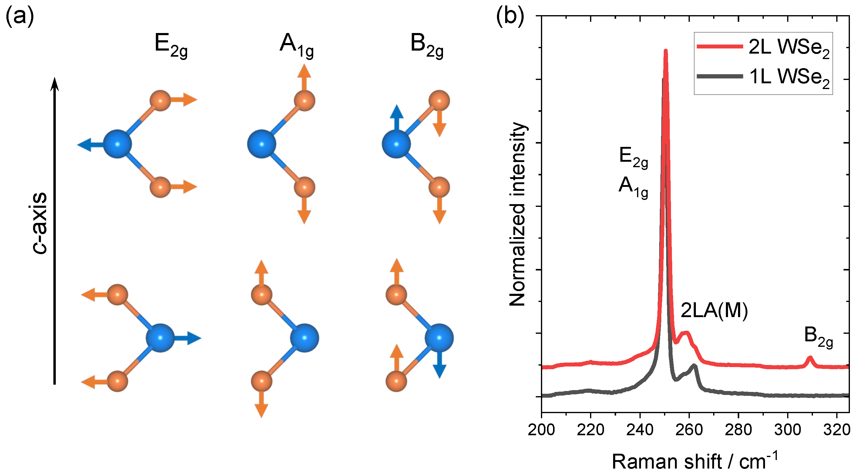
Figure 2.
Raman and PL measurements of monolayer and bilayer WSe. (a) Optical microscope image of monolayer and bilayer WSe. Raman intensity map of the WSe peak (304–314 cm) (b) before and (c) after annealing. (b,c) share the same color scale. (d) Raman spectra of monolayer and bilayer WSe before and after annealing. PL intensity map of WSe A exciton (1.60–1.75 eV) (e) before and (f) after annealing. (g) PL spectra of monolayer and bilayer WSe before and after annealing. Inset: as-measured (not-normalized) PL spectra. The scale bar in figure is 5 µm.
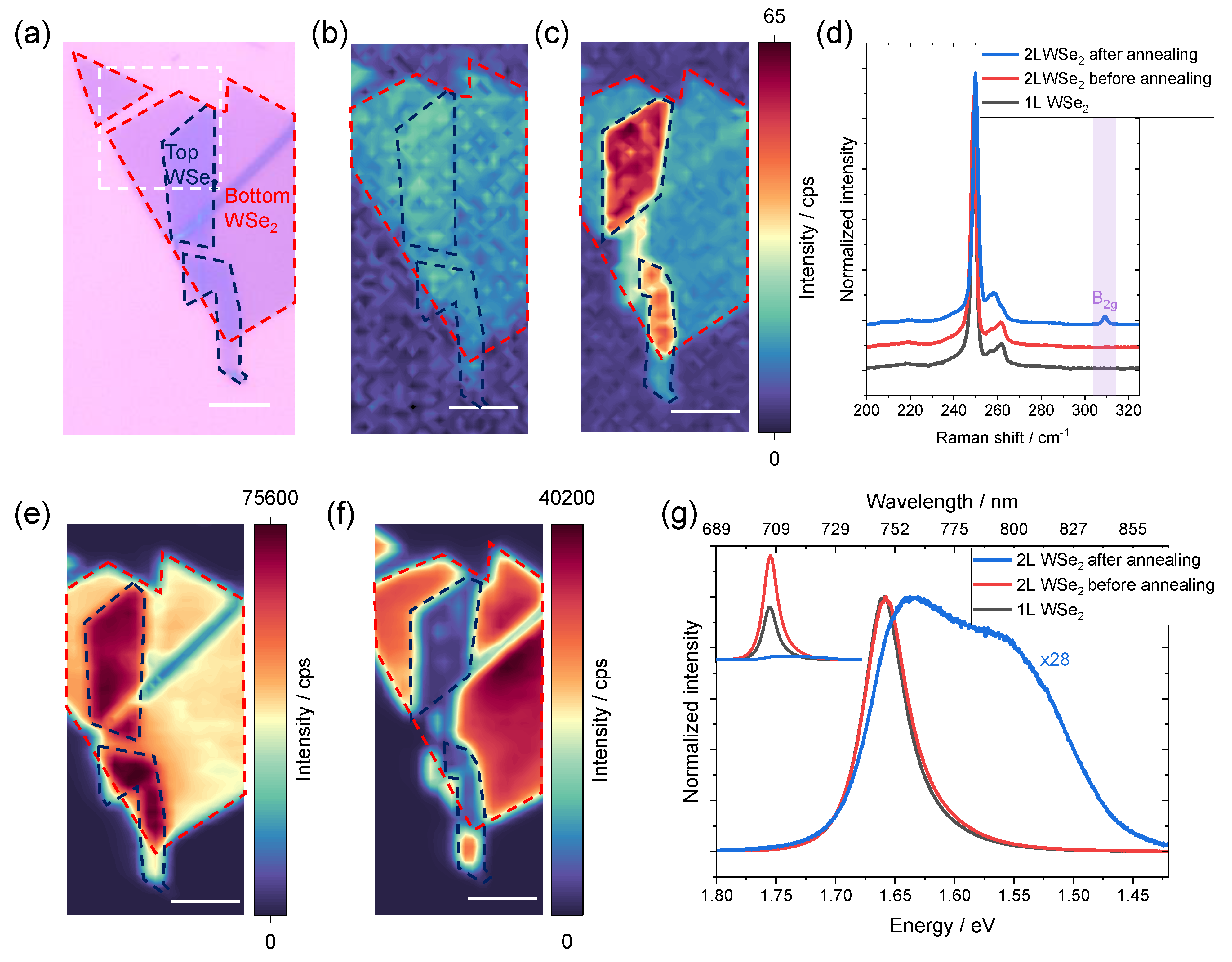
Figure 3.
AFM of monolayer and bilayer WSe (a) before and (b) after annealing. (a,b) share the same color scale. The measured area corresponds to the white squared area in Figure 2a. (c) Schematic diagram of the AFM profile. (d) Height profile of monolayer and bilayer WSe before and after annealing. Scale bar in figure is 4 µm.
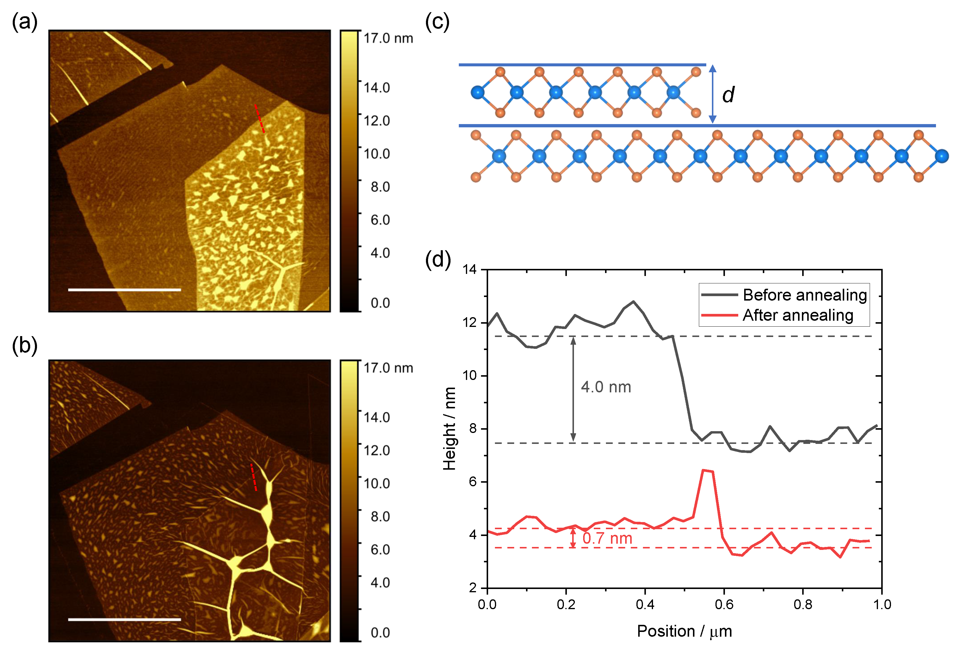
Figure 4.
(a) Raman spectra of monolayer and bilayer MoSe. (b) Raman and (c) PL spectra of monolayer WSe, MoSe, and MoSe/WSe hetero-bilayer before and after annealing. The spectra between 1.80 eV and 1.45 eV are normalized from 0 to 1, and the spectra between 1.45 eV and 1.23 eV are normalized from 0 to 0.4 for better visualization. Inset: as-measured (not-normalized) PL spectra.

Publisher’s Note: MDPI stays neutral with regard to jurisdictional claims in published maps and institutional affiliations. |
© 2022 by the authors. Licensee MDPI, Basel, Switzerland. This article is an open access article distributed under the terms and conditions of the Creative Commons Attribution (CC BY) license (https://creativecommons.org/licenses/by/4.0/).
Share and Cite
MDPI and ACS Style
Pan, Y.; Zahn, D.R.T. Raman Fingerprint of Interlayer Coupling in 2D TMDCs. Nanomaterials 2022, 12, 3949. https://doi.org/10.3390/nano12223949
AMA Style
Pan Y, Zahn DRT. Raman Fingerprint of Interlayer Coupling in 2D TMDCs. Nanomaterials. 2022; 12(22):3949. https://doi.org/10.3390/nano12223949
Chicago/Turabian StylePan, Yang, and Dietrich R. T. Zahn. 2022. "Raman Fingerprint of Interlayer Coupling in 2D TMDCs" Nanomaterials 12, no. 22: 3949. https://doi.org/10.3390/nano12223949
Note that from the first issue of 2016, this journal uses article numbers instead of page numbers. See further details here.