
Recent Advancements in Tin Halide Perovskite-Based Solar Cells and Thermoelectric Devices

Abstract
:
1. Introduction
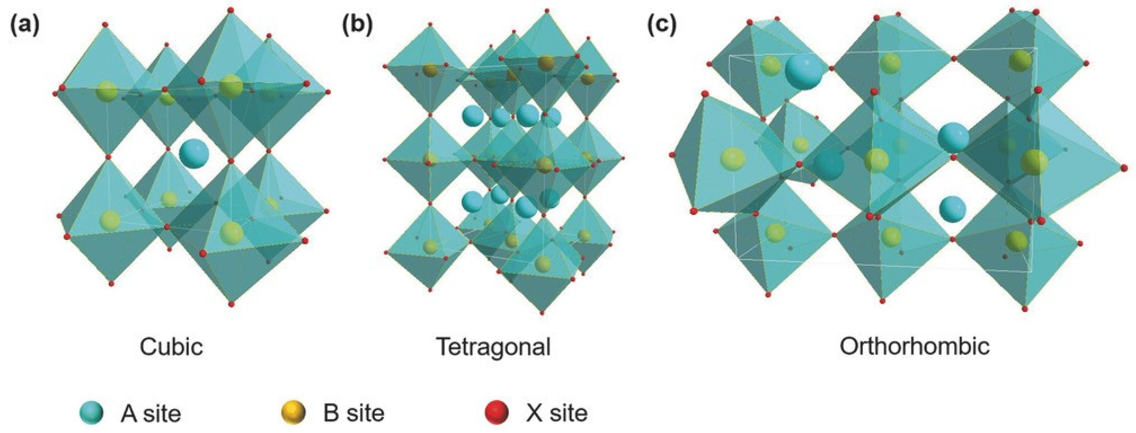
1.1. Structural Properties
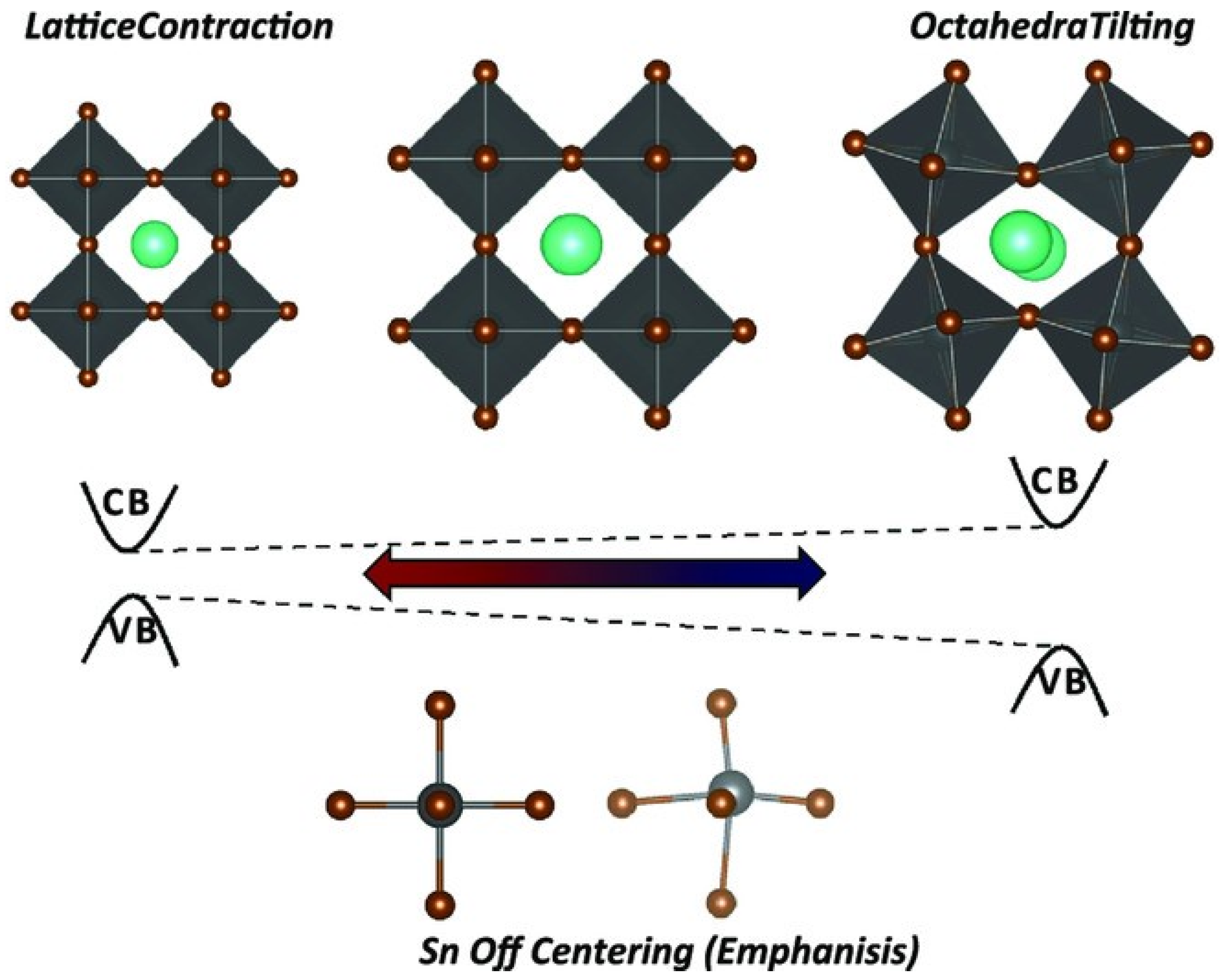
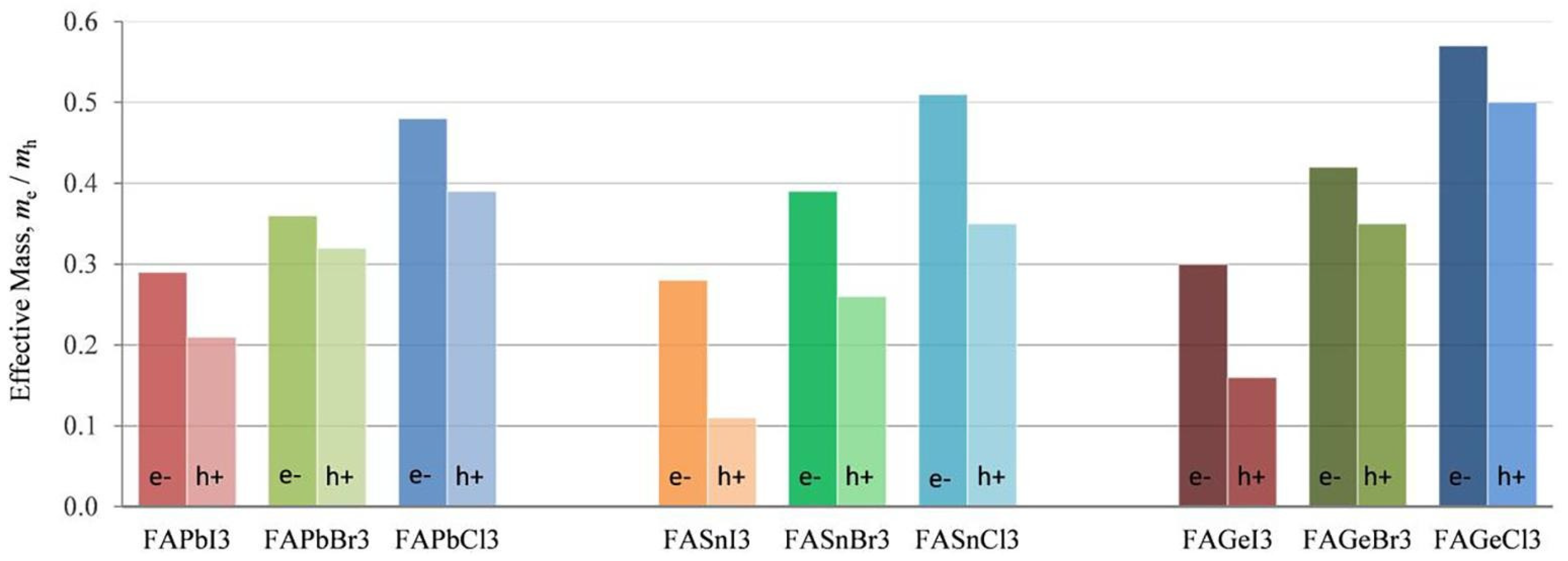
1.2. Electronic and Optical Properties
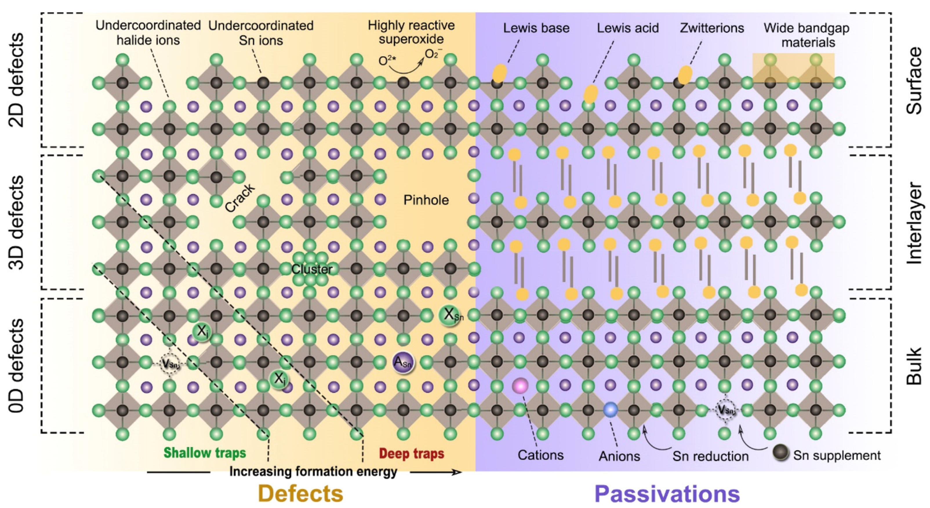
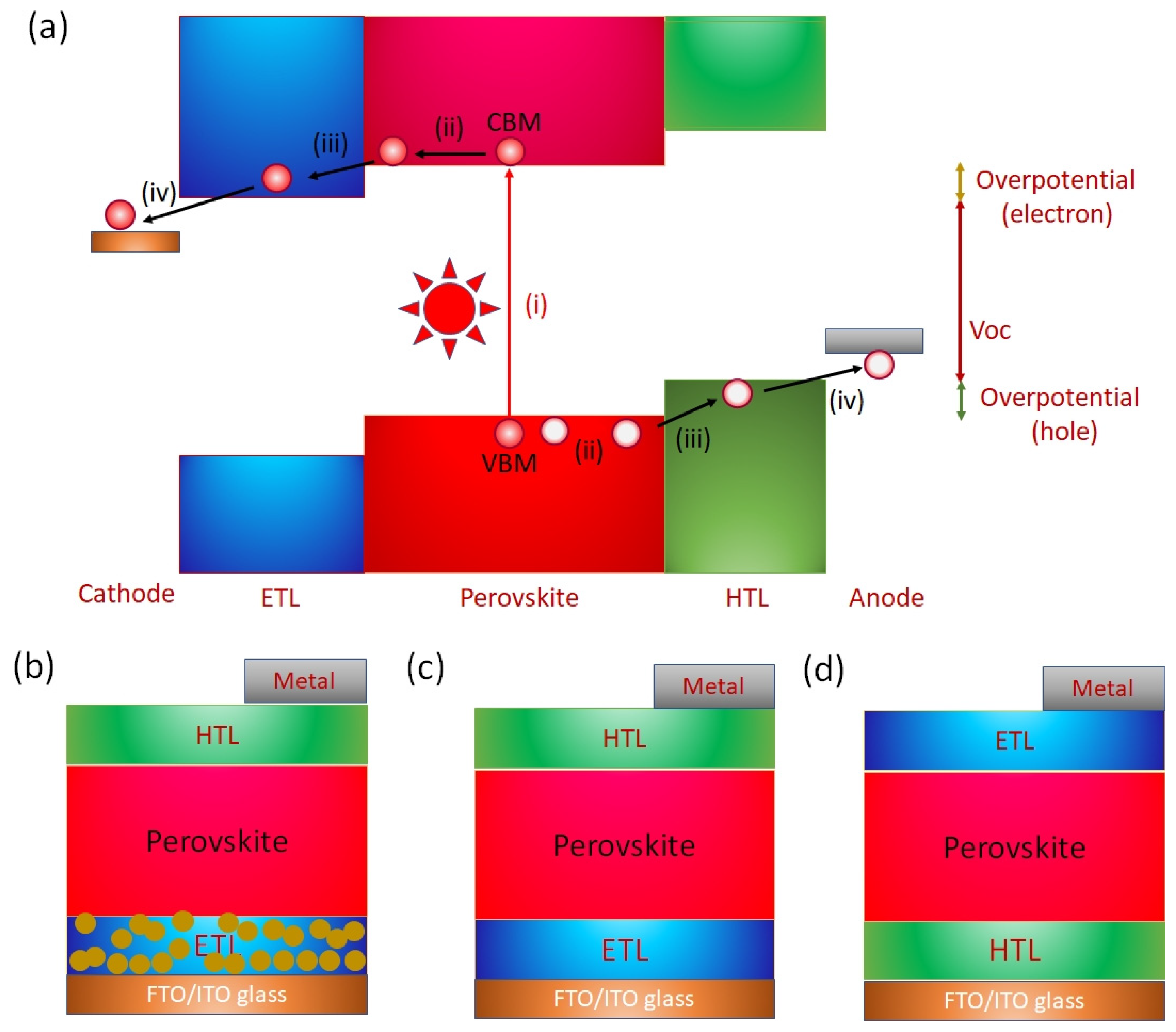
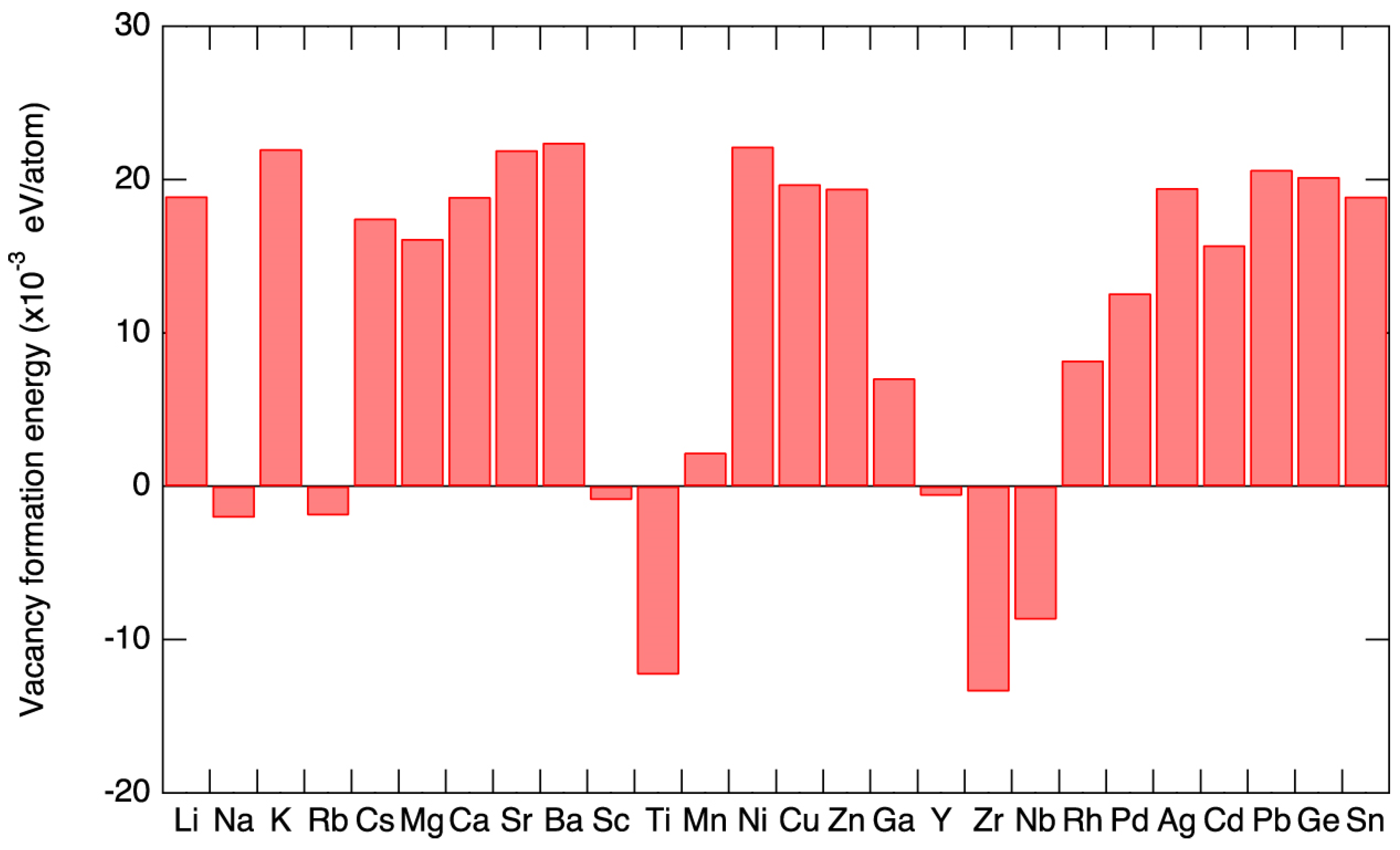
1.3. Defect Physics and Charge Transport
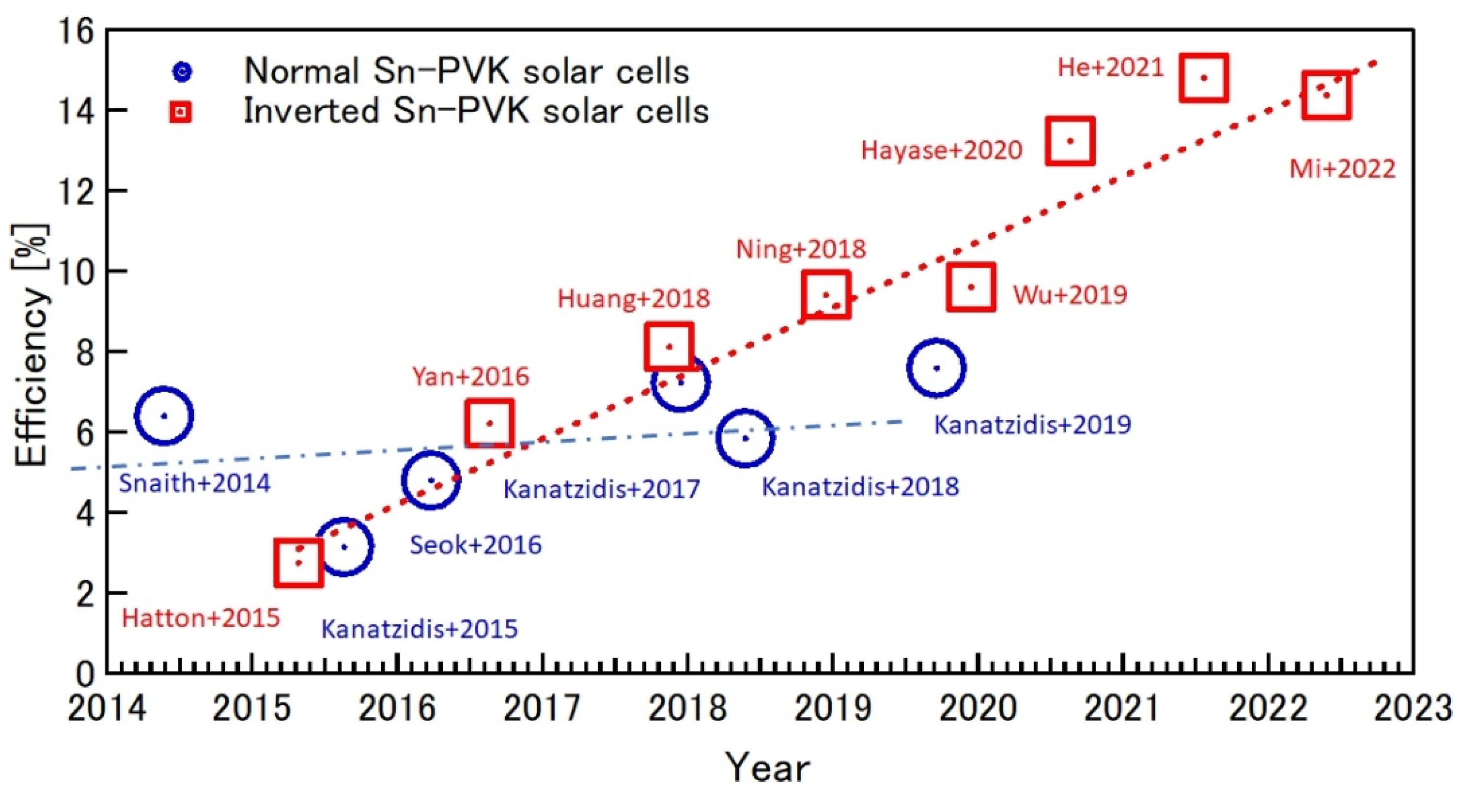
2. Solar Cells
2.1. Normal Structure
2.2. Inverted Structure
2.2.1. Device Engineering
2.2.2. A 2D/3D Photoactive Layer
2.2.3. Surface Passivation of Photoactive Layer
2.2.4. A-Site Substitution
2.2.5. Vacuum-Assisted Strategy
2.2.6. Solution Engineering
2.2.7. Additive Technology
2.2.8. Three-Layer Mesoscopic Solar Cell
2.2.9. ETL/HTL Modification
2.2.10. Flexible FASnI3 Solar Cell
2.2.11. Electrode Engineering
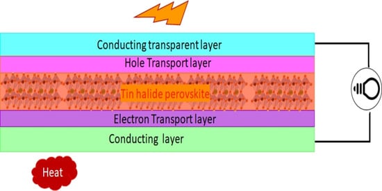
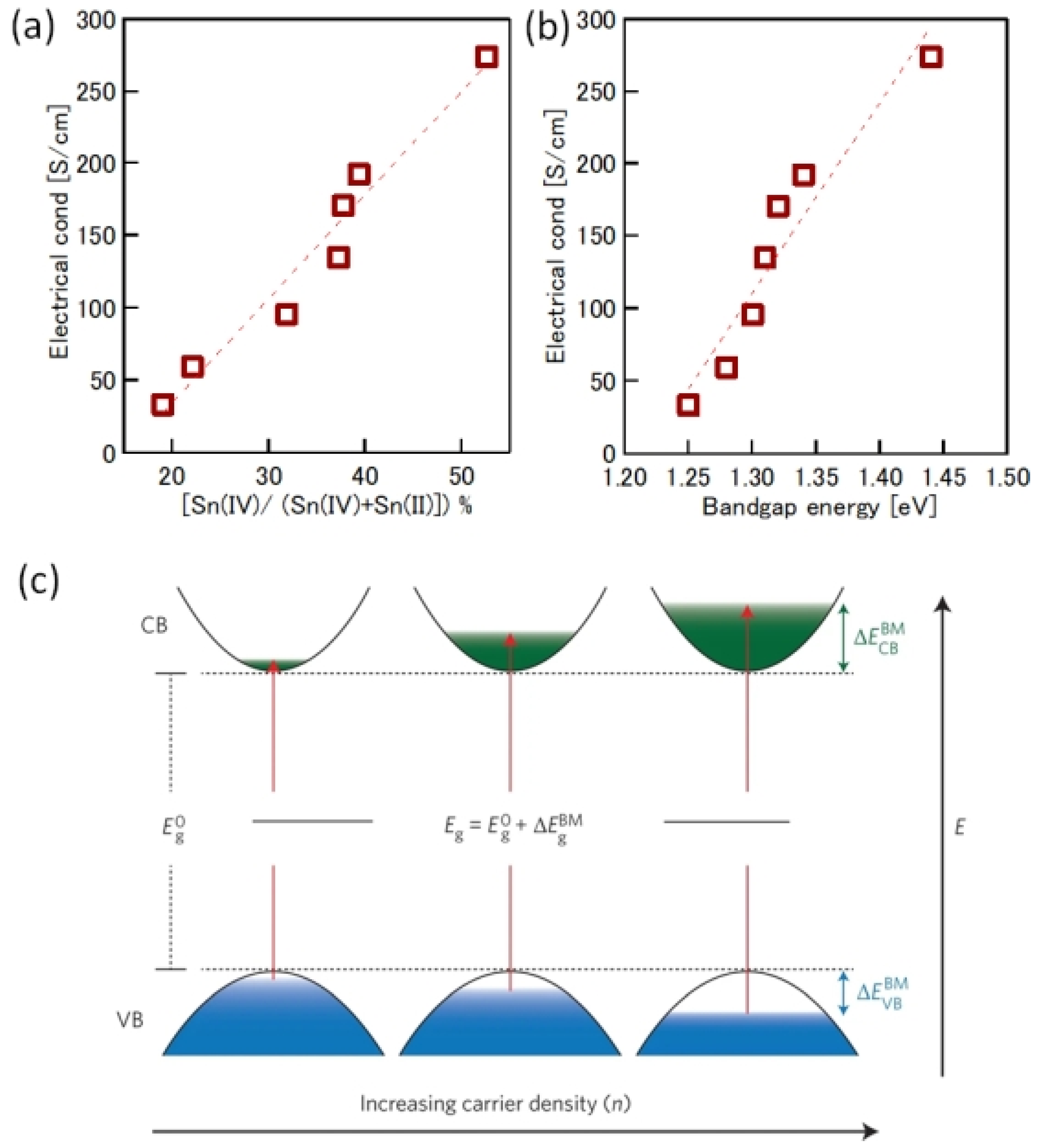
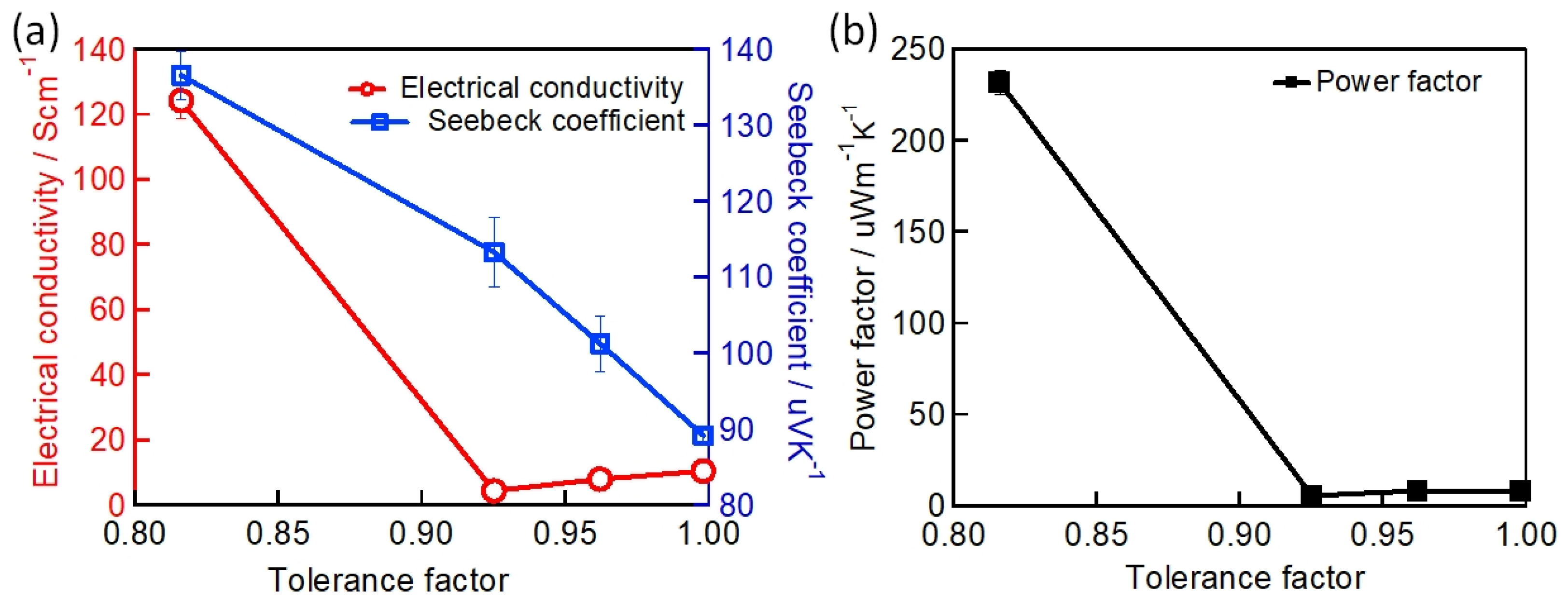
3. Thermoelectric Devices
3.1. CsSnI3 Thermoelectric Film
3.2. FASnI3 Thermoelectric Film
3.3. MASnI3 Thermoelectric Film
4. Challenges and Remedies
5. Conclusions
Author Contributions
Funding
Institutional Review Board Statement
Informed Consent Statement
Data Availability Statement
Conflicts of Interest
References
- Stranks, S.D.; Eperon, G.E.; Grancini, G.; Menelaou, C.; Alcocer, M.J.P.; Leijtens, T.; Herz, L.M.; Petrozza, A.; Snaith, H.J. Electron-Hole Diffusion Lengths Exceeding 1 Micrometer in an Organometal Trihalide Perovskite Absorber. Science 2013, 342, 341–344. [Google Scholar] [CrossRef] [PubMed] [Green Version]
- Haque, M.A.; Kee, S.; Villalva, D.R.; Ong, W.; Baran, D. Halide Perovskites: Thermal Transport and Prospects for Thermoelectricity. Adv. Sci. 2020, 7, 1903389. [Google Scholar] [CrossRef] [PubMed] [Green Version]
- Ng, Y.F.; Kulkarni, S.A.; Parida, S.; Jamaludin, N.F.; Yantara, N.; Bruno, A.; Soci, C.; Mhaisalkar, S.; Mathews, N. Highly efficient Cs-based perovskite light-emitting diodes enabled by energy funnelling. Chem. Commun. 2017, 53, 12004–12007. [Google Scholar] [CrossRef]
- Veldhuis, S.A.; Boix, P.P.; Yantara, N.; Li, M.; Sum, T.C.; Mathews, N.; Mhaisalkar, S.G. Perovskite Materials for Light-Emitting Diodes and Lasers. Adv. Mater. 2016, 28, 6804–6834. [Google Scholar] [CrossRef]
- Kim, Y.-J.; Dang, T.-V.; Choi, H.-J.; Park, B.-J.; Eom, J.-H.; Song, H.-A.; Seol, D.; Kim, Y.; Shin, S.-H.; Nah, J.; et al. Piezoelectric properties of CH3NH3 PbI3 perovskite thin films and their applications in piezoelectric generators. J. Mater. Chem. A 2016, 4, 756–763. [Google Scholar] [CrossRef]
- He, X.; Qiu, Y.; Yang, S. Fully-Inorganic Trihalide Perovskite Nanocrystals: A New Research Frontier of Optoelectronic Materials. Adv. Mater. 2017, 29, 1700775. [Google Scholar] [CrossRef]
- Zhou, Y.; Parkes, M.A.; Zhang, J.; Wang, Y.; Ruddlesden, M.; Fielding, H.H.; Su, L. Single-crystal organometallic perovskite optical fibers. Sci. Adv. 2022, 8, eabq8629. [Google Scholar] [CrossRef]
- Available online: https://www.nrel.gov/pv/cell-efficiency.html (accessed on 19 October 2022).
- Kojima, A.; Teshima, K.; Shirai, Y.; Miyasaka, T. Organometal halide perovskites as visible-light sensitizers for photovoltaic cells. J. Am. Chem. Soc. 2009, 131, 6050–6051. [Google Scholar] [CrossRef]
- Green, M.A.; Dunlop, E.D.; Hohl-Ebinger, J.; Yoshita, M.; Kopidakis, N.; Hao, X. Solar cell efficiency tables (version 59). Prog. Photovolt. Res. Appl. 2022, 30, 3–12. [Google Scholar] [CrossRef]
- McMeekin, D.P.; Sadoughi, G.; Rehman, W.; Eperon, G.E.; Saliba, M.; Horantner, M.T.; Haghighirad, A.; Sakai, N.; Korte, L.; Rech, B.; et al. A mixed-cation lead mixed-halide perovskite absorber for tandem solar cells. Science 2016, 351, 151–155. [Google Scholar] [CrossRef]
- Tan, H.; Jain, A.; Voznyy, O.; Lan, X.; García de Arquer, F.P.; Fan, J.Z.; Quintero-Bermudez, R.; Yuan, M.; Zhang, B.; Zhao, Y.; et al. Efficient and stable solution-processed planar perovskite solar cells via contact passivation. Science 2017, 355, 722–726. [Google Scholar] [CrossRef] [PubMed]
- Bi, D.; Tress, W.; Dar, M.I.; Gao, P.; Luo, J.; Renevier, C.; Schenk, K.; Abate, A.; Giordano, F.; Correa Baena, J.-P.; et al. Efficient luminescent solar cells based on tailored mixed-cation perovskites. Sci. Adv. 2016, 2, e1501170. [Google Scholar] [CrossRef] [Green Version]
- Baranwal, A.K.; Masutani, H.; Sugita, H.; Kanda, H.; Kanaya, S.; Shibayama, N.; Sanehira, Y.; Ikegami, M.; Numata, Y.; Yamada, K.; et al. Lead-free perovskite solar cells using Sb and Bi-based A3B2X9 and A3BX6 crystals with normal and inverse cell structures. Nano Converg. 2017, 4, 26. [Google Scholar] [CrossRef] [PubMed] [Green Version]
- Ke, W.; Stoumpos, C.C.; Kanatzidis, M.G. “Unleaded” Perovskites: Status Quo and Future Prospects of Tin-Based Perovskite Solar Cells. Adv. Mater. 2019, 31, 1803230. [Google Scholar] [CrossRef] [PubMed]
- Chen, M.; Ju, M.-G.; Carl, A.D.; Zong, Y.; Grimm, R.L.; Gu, J.; Zeng, X.C.; Zhou, Y.; Padture, N.P. Cesium Titanium(IV) Bromide Thin Films Based Stable Lead-free Perovskite Solar Cells. Joule 2018, 2, 558–570. [Google Scholar] [CrossRef] [Green Version]
- Kopacic, I.; Friesenbichler, B.; Hoefler, S.F.; Kunert, B.; Plank, H.; Rath, T.; Trimmel, G. Enhanced Performance of Germanium Halide Perovskite Solar Cells through Compositional Engineering. ACS Appl. Energy Mater. 2018, 1, 343–347. [Google Scholar] [CrossRef]
- Ahmad, K.; Mobin, S.M. Organic–Inorganic Copper (II)-Based Perovskites: A Benign Approach toward Low-Toxicity and Water-Stable Light Absorbers for Photovoltaic Applications. Energy Technol. 2020, 8, 1901185. [Google Scholar] [CrossRef]
- Konstantakou, M.; Stergiopoulos, T. A critical review on tin halide perovskite solar cells. J. Mater. Chem. A 2017, 5, 11518–11549. [Google Scholar] [CrossRef]
- Yu, B.; Chen, Z.; Zhu, Y.; Wang, Y.; Han, B.; Chen, G.; Zhang, X.; Du, Z.; He, Z. Heterogeneous 2D/3D Tin-Halides Perovskite Solar Cells with Certified Conversion Efficiency Breaking 14%. Adv. Mater. 2021, 33, 2102055. [Google Scholar] [CrossRef]
- Lee, W.; Li, H.; Wong, A.B.; Zhang, D.; Lai, M.; Yu, Y.; Kong, Q.; Lin, E.; Urban, J.J.; Grossman, J.C.; et al. Ultralow thermal conductivity in all-inorganic halide perovskites. Proc. Natl. Acad. Sci. USA 2017, 114, 8693–8697. [Google Scholar] [CrossRef]
- Zhou, F.; Qin, F.; Yi, Z.; Yao, W.; Liu, Z.; Wu, X.; Wu, P. Ultra-wideband and wide-angle perfect solar energy absorber based on Ti nanorings surface plasman resonance. Phys. Chem. Chem. Phys. 2021, 23, 17041. [Google Scholar] [CrossRef] [PubMed]
- Wu, J.; Sun, Y.; Wu, B.; Sun, C.; Wu, X. Perfect metamaterial absorber for solar energy utilization. Int. J. Thermal Sci. 2022, 179, 107638. [Google Scholar] [CrossRef]
- Wu, J.; Sun, Y.; Wu, B.; Sun, C.; Wu, X. Broadband and wide-angle solar absorber for the visible and near-infrared frequencies. Solar Energy 2022, 238, 78–83. [Google Scholar] [CrossRef]
- Shi, T.; Zhang, H.-S.; Meng, W.; Teng, Q.; Liu, M.; Yang, X.; Yan, Y.; Yip, H.-L.; Zhao, Y.-J. Effects of organic cations on the defect physics of tin halide perovskites. J. Mater. Chem. A 2017, 5, 15124–15129. [Google Scholar] [CrossRef]
- Liu, Y.; Yang, Z.; Liu, S.F. Recent Progress in Single-Crystalline Perovskite Research Including Crystal Preparation, Property Evaluation, and Applications. Adv. Sci. 2018, 5, 1700471. [Google Scholar] [CrossRef]
- Saliba, M.; Matsui, T.; Domanski, K.; Seo, J.-Y.; Ummadisingu, A.; Zakeeruddin, S.M.; Correa-Baena, J.-P.; Tress, W.R.; Abate, A.; Hagfeldt, A.; et al. Incorporation of rubidium cations into perovskite solar cells improves photovoltaic performance. Science 2016, 354, 206–209. [Google Scholar] [CrossRef]
- Awais, M.; Kirsch, R.L.; Yeddu, V.; Saidaminov, M.I. Tin Halide Perovskites Going Forward: Frost Diagrams Offer Hints. ACS Mater. Lett. 2021, 3, 299–307. [Google Scholar] [CrossRef]
- Tao, S.; Schmidt, I.; Brocks, G.; Jiang, J.; Tranca, I.; Meerholz, K.; Olthof, S. Absolute energy level positions in tin- and lead-based halide perovskites. Nat. Commun. 2019, 10, 2560. [Google Scholar] [CrossRef] [Green Version]
- Bernal, C.; Yang, K. First-Principles Hybrid Functional Study of the Organic–Inorganic Perovskites CH3NH3SnBr3 and CH3 NH3SnI3. J. Phys. Chem. C 2014, 118, 24383–24388. [Google Scholar] [CrossRef]
- Di Girolamo, D.; Blundo, E.; Folpini, G.; Ponti, C.; Li, G.; Aldamasy, M.H.; Iqbal, Z.; Pascual, J.; Nasti, G.; Li, M.; et al. Energy Distribution in Tin Halide Perovskite. Sol. RRL 2022, 6, 2100825. [Google Scholar] [CrossRef]
- Roknuzzaman, M.; Alarco, J.A.; Wang, H.; Du, A.; Tesfamichael, T.; Ostrikov, K. Ab initio atomistic insights into lead-free formamidinium based hybrid perovskites for photovoltaics and optoelectronics. Comput. Mater. Sci. 2019, 169, 109118. [Google Scholar] [CrossRef]
- Huang, L.; Lambrecht, W.R.L. Electronic Band Structure, Phonons, and Exciton Binding Energies of Halide Perovskites CsSnCl3, CsSnBr3. Phys. Rev. B 2013, 88, 165203. [Google Scholar] [CrossRef]
- Ma, Z.-Q.; Pan, H.; Wong, P.K. A First-Principles Study on the Structural and Electronic Properties of Sn-Based Organic–Inorganic Halide Perovskites. J. Electron. Mater. 2016, 45, 5956–5966. [Google Scholar] [CrossRef]
- Chung, I.; Song, J.-H.; Im, J.; Androulakis, J.; Malliakas, C.D.; Li, H.; Freeman, A.J.; Kenney, J.T.; Kanatzidis, M.G. CsSnI3: Semiconductor or Metal? High Electrical Conductivity and Strong Near-Infrared Photoluminescence from a Single Material. High Hole Mobility and Phase-Transitions. J. Am. Chem. Soc. 2012, 134, 8579–8587. [Google Scholar] [CrossRef]
- Kahmann, S.; Shao, S.; Loi, M.A. Cooling, Scattering, and Recombination—The Role of the Material Quality for the Physics of Tin Halide Perovskites. Adv. Funct. Mater. 2019, 29, 1902963. [Google Scholar] [CrossRef] [Green Version]
- Milot, R.L.; Klug, M.T.; Davies, C.L.; Wang, Z.; Kraus, H.; Snaith, H.J.; Johnston, M.B.; Herz, L.M. The Effects of Doping Density and Temperature on the Optoelectronic Properties of Formamidinium Tin Triiodide Thin Films. Adv. Mater. 2018, 30, 1804506. [Google Scholar] [CrossRef] [Green Version]
- Baranwal, A.K.; Saini, S.; Wang, Z.; Hamada, K.; Hirotani, D.; Nishimura, K.; Kamarudin, M.A.; Kapil, G.; Yabuki, T.; Iikubo, S.; et al. Effect of Precursor Solution Aging on the Thermoelectric Performance of CsSnI3 Thin Film. J. Electron. Mater. 2020, 49, 2698–2703. [Google Scholar] [CrossRef]
- Ozaki, M.; Katsuki, Y.; Liu, J.; Handa, T.; Nishikubo, R.; Yakumaru, S.; Hashikawa, Y.; Murata, Y.; Saito, T.; Shimakawa, Y.; et al. Solvent-Coordinated Tin Halide Complexes as Purified Precursors for Tin-Based Perovskites. ACS Omega 2017, 2, 7016–7021. [Google Scholar] [CrossRef] [Green Version]
- Kumar Baranwal, A.; Saini, S.; Sanehira, Y.; Kapil, G.; Akmal Kamarudin, M.; Ding, C.; Razey Sahamir, S.; Yabuki, T.; Iikubo, S.; Shen, Q.; et al. Unveiling the Role of the Metal Oxide/Sn Perovskite Interface Leading to Low Efficiency of Sn-Perovskite Solar Cells but Providing High Thermoelectric Properties. ACS Appl. Energy Mater. 2022, 5, 9750–9758. [Google Scholar] [CrossRef]
- Manser, J.S.; Kamat, P.V. Band filling with free charge carriers in organometal halide perovskites. Nat. Photonics 2014, 8, 737–743. [Google Scholar] [CrossRef]
- El Ajjouri, Y.; Locardi, F.; Gélvez-Rueda, M.C.; Prato, M.; Sessolo, M.; Ferretti, M.; Grozema, F.C.; Palazon, F.; Bolink, H.J. Mechanochemical Synthesis of Sn(II) and Sn(IV) Iodide Perovskites and Study of Their Structural, Chemical, Thermal, Optical and Electrical Properties. Energy Technol. 2019, 1900788, 1900788. [Google Scholar] [CrossRef]
- Xu, P.; Chen, S.; Xiang, H.-J.; Gong, X.-G.; Wei, S.-H. Influence of Defects and Synthesis Conditions on the Photovoltaic Performance of Perovskite Semiconductor CsSnI3. Chem. Mater. 2014, 26, 6068–6072. [Google Scholar] [CrossRef]
- Kumar, M.H.; Dharani, S.; Leong, W.L.; Boix, P.P.; Prabhakar, R.R.; Baikie, T.; Shi, C.; Ding, H.; Ramesh, R.; Asta, M.; et al. Lead-free halide perovskite solar cells with high photocurrents realized through vacancy modulation. Adv. Mater. 2014, 26, 7122–7127. [Google Scholar] [CrossRef] [PubMed]
- Ulatowski, A.M.; Farrar, M.D.; Snaith, H.J.; Johnston, M.B.; Herz, L.M. Revealing Ultrafast Charge-Carrier Thermalization in Tin-Iodide Perovskites through Novel Pump–Push–Probe Terahertz Spectroscopy. ACS Photonics 2021, 8, 2509–2518. [Google Scholar] [CrossRef] [PubMed]
- Li, B.; Chang, B.; Pan, L.; Li, Z.; Fu, L.; He, Z.; Yin, L. Tin-Based Defects and Passivation Strategies in Tin-Related Perovskite Solar Cells. ACS Energy Lett. 2020, 5, 3752–3772. [Google Scholar] [CrossRef]
- Wolff, C.M.; Bourelle, S.A.; Phuong, L.Q.; Kurpiers, J.; Feldmann, S.; Caprioglio, P.; Marquez, J.A.; Wolansky, J.; Unold, T.; Stolterfoht, M.; et al. Orders of Recombination in Complete Perovskite Solar Cells-Linking Time-Resolved and Steady-State Measurements. Adv. Energy Mater. 2021, 11, 2101823. [Google Scholar] [CrossRef]
- Noel, N.K.; Stranks, S.D.; Abate, A.; Wehrenfennig, C.; Guarnera, S.; Haghighirad, A.-A.; Sadhanala, A.; Eperon, G.E.; Pathak, S.K.; Johnston, M.B.; et al. Lead-free organic–inorganic tin halide perovskites for photovoltaic applications. Energy Environ. Sci. 2014, 7, 3061–3068. [Google Scholar] [CrossRef]
- Wang, L.; Chen, M.; Yang, S.; Uezono, N.; Miao, Q.; Kapil, G.; Baranwal, A.K.; Sanehira, Y.; Wang, D.; Liu, D.; et al. SnO x as Bottom Hole Extraction Layer and Top In Situ Protection Layer Yields over 14% Efficiency in Sn-Based Perovskite Solar Cells. ACS Energy Lett. 2022, 7, 3703–3708. [Google Scholar] [CrossRef]
- Jiang, Y.; Lu, Z.; Zou, S.; Lai, H.; Zhang, Z.; Luo, J.; Huang, Y.; He, R.; Jin, J.; Yi, Z.; et al. Dual-site passivation of tin-related defects enabling efficient lead-free tin perovskite solar cells. Nano Energy 2022, 103, 107818. [Google Scholar] [CrossRef]
- Zhu, Z.; Jiang, X.; Yu, D.; Yu, N.; Ning, Z.; Mi, Q. Smooth and Compact FASnI3 Films for Lead-Free Perovskite Solar Cells with over 14% Efficiency. ACS Energy Lett. 2022, 7, 2079–2083. [Google Scholar] [CrossRef]
- Li, B.; Wu, X.; Zhang, H.; Zhang, S.; Li, Z.; Gao, D.; Zhang, C.; Chen, M.; Xiao, S.; Jen, A.K.Y.; et al. Efficient and Stable Tin Perovskite Solar Cells by Pyridine-Functionalized Fullerene with Reduced Interfacial Energy Loss. Adv. Funct. Mater. 2022, 2205870, 2205870. [Google Scholar] [CrossRef]
- Nishimura, K.; Kamarudin, M.A.; Hirotani, D.; Hamada, K.; Shen, Q.; Iikubo, S.; Minemoto, T.; Yoshino, K.; Hayase, S. Lead-free tin-halide perovskite solar cells with 13% efficiency. Nano Energy 2020, 74, 104858. [Google Scholar] [CrossRef]
- Zou, S.; Ren, S.; Jiang, Y.; Huang, Y.; Wang, W.; Wang, C.; Chen, C.; Hao, X.; Wu, L.; Zhang, J.; et al. Efficient Environment-friendly Lead-free Tin Perovskite Solar Cells Enabled by Incorporating 4-Fluorobenzylammonium Iodide Additives. Energy Environ. Mater. 2022, e12465. [Google Scholar] [CrossRef]
- Wang, T.; Loi, H.; Cao, J.; Qin, Z.; Guan, Z.; Xu, Y.; Cheng, H.; Li, M.G.; Lee, C.; Lu, X.; et al. High Open Circuit Voltage Over 1 V Achieved in Tin-Based Perovskite Solar Cells with a 2D/3D Vertical Heterojunction. Adv. Sci. 2022, 9, 2200242. [Google Scholar] [CrossRef] [PubMed]
- Zhang, Z.; Kamarudin, M.A.; Baranwal, A.K.; Kapil, G.; Sahamir, S.R.; Sanehira, Y.; Chen, M.; Wang, L.; Shen, Q.; Hayase, S. Sequential Passivation for Lead-Free Tin Perovskite Solar Cells with High Efficiency. Angew. Chem. 2022, 61, e202210101. [Google Scholar] [CrossRef]
- Liu, G.; Zhong, Y.; Feng, W.; Yang, M.; Yang, G.; Zhong, J.; Tian, T.; Luo, J.; Tao, J.; Yang, S.; et al. Multidentate Chelation Heals Structural Imperfections for Minimized Recombination Loss in Lead-Free Perovskite Solar Cells. Angew. Chemie 2022, 61, e202209464. [Google Scholar] [CrossRef]
- Zhang, W.; Cai, Y.; Liu, H.; Xia, Y.; Cui, J.; Shi, Y.; Chen, R.; Shi, T.; Wang, H. Organic-Free and Lead-Free Perovskite Solar Cells with Efficiency over 11%. Adv. Energy Mater. 2022, 2202491, 2202491. [Google Scholar] [CrossRef]
- Jokar, E.; Chuang, H.-S.; Kuan, C.-H.; Wu, H.-P.; Hou, C.-H.; Shyue, J.-J.; Wei-Guang Diau, E. Slow Passivation and Inverted Hysteresis for Hybrid Tin Perovskite Solar Cells Attaining 13.5% via Sequential Deposition. J. Phys. Chem. Lett. 2021, 12, 10106–10111. [Google Scholar] [CrossRef]
- Jiang, X.; Li, H.; Zhou, Q.; Wei, Q.; Wei, M.; Jiang, L.; Wang, Z.; Peng, Z.; Wang, F.; Zang, Z.; et al. One-Step Synthesis of SnI 2·(DMSO)x Adducts for High-Performance Tin Perovskite Solar Cells. J. Am. Chem. Soc. 2021, 143, 10970–10976. [Google Scholar] [CrossRef]
- Marshall, K.P.; Walton, R.; Hatton, R.A. Tin Perovskite/Fullerene Planar Layer Photovoltaics: Improving the Efficiency and Stability of Lead-free Devices. J. Mater. Chem. A 2015, 3, 11631–11640. [Google Scholar] [CrossRef]
- Hao, H.; Stoumpos, C.C.; Guo, P.; Zhou, N.; Marks, T.J.; Chang, R.P.H.; Kanatzidis, M.G. Solvent-Mediated Crystallization of CH3NH3SnI3 Films for Heterojunction Depleted Perovskite Solar Cells. J. Am. Chem. Soc. 2015, 137, 11445–11452. [Google Scholar] [CrossRef] [PubMed]
- Lee, S.J.; Shin, S.S.; Kim, Y.C.; Kim, D.; Ahn, T.K.; Noh, J.H.; Seo, J.; Seok, S.I. Fabrication of Efficient Formamidinium Tin Iodide Perovskite Solar Cells through SnF2-Pyrazine. J. Am. Chem. Soc. 2016, 138, 3974–3977. [Google Scholar] [CrossRef] [PubMed]
- Liao, W.; Zhao, D.; Yu, Y.; Grice, C.R.; Wang, C.; Cimaroli, A.J.; Schulz, P.; Meng, W.; Zhu, K.; Xiong, R.-G.; et al. Lead-Free Inverted Planar Formamidinium Tin Triiodide Perovskite Solar Cells Achieving Power Conversion Efficiencies up to 6.22%. Adv. Mater. 2016, 28, 9333–9340. [Google Scholar] [CrossRef] [PubMed]
- Ke, W.; Stoumpos, C.C.; Spanopoulos, I.; Chen, M.; Wasielewski, M.R.; Kanatzidis, M.G. Diammonium Cations in the FASnI3 perovskite Structure Lead to Lower Dark Currents and More Efficient Solar Cells. ACS Energy Lett. 2018, 3, 1470–1476. [Google Scholar] [CrossRef]
- Ke, W.; Priyanka, P.; Vegiraju, S.; Stoumpos, C.C.; Spanopoulos, I.; Soe, C.M.M.; Marks, T.J.; Chen, M.-C.; Kanatzidis, M.G. Dopant-Free Tetrakis-Triphenylamine Hole Transporting Material for Efficient Tin-Based Perovskite Solar Cells. J. Am. Chem. Soc. 2018, 140, 388–393. [Google Scholar] [CrossRef]
- Ziran, Z.; Gu, F.; Li, Y.; Sun, W.; Ye, S.; Rao, H.; Liu, Z.; Bian, Z.; Huang, C. Mixed Organic-Cation Tin Iodide for Lead-free Perovskite Solar Cells with an Efficiency of 8.12%. Adv. Sci. 2017, 4, 1700204. [Google Scholar]
- Vegiraju, S.; Ke, W.; Priyanka, P.; Ni, J.-S.; Wu, Y.-C.; Spanopoulos, I.; Yau, S.L.; Marks, T.; Chen, M.-C.; Kanatzidis, M.G. Benzodithiophene Hole-Transporting Materials for Efficient Tin-Based Perovskite Solar Cells. Adv. Funct. Mater. 2019, 29, 1905393. [Google Scholar] [CrossRef]
- Wang, F.; Jiang, X.; Chen, H.; Shang, Y.; Liu, H.; Wei, J.; Zhou, W.; He, H.; Liu, W.; Ning, Z. 2D-Quasi-2D-3D Hierarchy Structure for Tin Perovskite Solar Cells with Enhanced Efficiency and Stability. Joule 2018, 2, 2732–2743. [Google Scholar] [CrossRef] [Green Version]
- Ran, C.; Gao, W.; Li, J.; Xi, J.; Li, L.; Dai, J.; Yang, Y.; Gao, X.; Dong, H.; Jiao, B.; et al. Conjugated Organic Cation Enable Efficienct Self-Healing FASnI3 Solar Cells. Joule 2019, 3, 3072–3087. [Google Scholar] [CrossRef]
- Ogomi, Y.; Morita, A.; Tsukamoto, S.; Saitho, T.; Fujikawa, N.; Shen, Q.; Toyoda, T.; Yoshino, K.; Pandey, S.S.; Ma, T.; et al. CH3NH3SnxPb(1–x)I3 Perovskite Solar Cells Covering up to 1060 Nm. J. Phys. Chem. Lett. 2014, 5, 1004–1011. [Google Scholar] [CrossRef]
- Wang, F.; Ma, J.; Xie, F.; Li, L.; Chen, J.; Fan, J.; Zhao, N. Organic Cation-Dependent Degradation Mechanism of Organotin Halide Perovskites. Adv. Funct. Mater. 2016, 26, 3417–3423. [Google Scholar] [CrossRef]
- Hamada, K.; Tanaka, R.; Kamarudin, M.A.; Shen, Q.; Iikubo, S.; Minemoto, T.; Yoshino, K.; Toyoda, T.; Ma, T.; Kang, D.-W.; et al. Enhanced Device Performance with Passivation of the TiO2 Surface Using a Carboxylic Acid Fullerene Monolayer for a SnPb Perovskite Solar Cell with a Normal Planar Structure. ACS Appl. Mater. Interfaces 2020, 12, 17776–17782. [Google Scholar] [CrossRef] [PubMed]
- Zhu, Z.; Chueh, C.; Li, N.; Mao, C.; Jen, A.K.Y. Realizing Efficient Lead-Free Formamidinium Tin Triiodide Perovskite Solar Cells via a Sequential Deposition Route. Adv. Mater. 2018, 30, 1703800. [Google Scholar] [CrossRef] [PubMed]
- Yang, Z.; Zhong, M.; Liang, Y.; Yang, L.; Liu, X.; Lin, Q.; Zhang, J.; Xu, D. SnO2-C60 Pyrrolidine Tris-Acid (CPTA) as the Electron Transport Layer for Highly Efficient and Stable Planar Sn-Based Perovskite Solar Cells. Adv. Funct. Mater. 2019, 29, 1903621. [Google Scholar] [CrossRef]
- Baranwal, A.K.; Saini, S.; Wang, Z.; Hirotani, D.; Yabuki, T.; Iikubo, S.; Miyazaki, K.; Hayase, S. Interface engineering using Y2O3 scaffold to enhance the thermoelectric performance of CsSnI3 thin film. Org. Electron. 2020, 76, 105488. [Google Scholar] [CrossRef]
- Chen, M.; Dong, Q.; Xiao, C.; Zheng, X.; Dai, Z.; Shi, Y.; Luther, J.M.; Padture, N.P. Lead-Free Flexible Perovskite Solar Cells with Interfacial Native Oxide Have >10% Efficiency and Simultaneously Enhanced Stability and Reliability. ACS Energy Lett. 2022, 7, 2256–2264. [Google Scholar] [CrossRef]
- Miyamoto, Y.; Kusumoto, S.; Yokoyama, T.; Nishitani, Y.; Matsui, T.; Kouzaki, T.; Nishikubo, R.; Saeki, A.; Kaneko, Y. High Current Density Sn-Based Perovskite Solar Cells via Enhanced Electron Extraction in Nanoporous Electron Transport Layers. ACS Appl. Nano Mater. 2020, 3, 11650–11657. [Google Scholar] [CrossRef]
- Zillner, J.; Boyen, H.; Schulz, P.; Hanisch, J.; Gauquelin, N.; Verbeeck, J.; Küffner, J.; Desta, D.; Eisele, L.; Ahlswede, E.; et al. The Role of SnF2 Additive on Interface Formation in All Lead-Free FASnI3 Perovskite Solar Cells. Adv. Funct. Mater. 2022, 32, 2109649. [Google Scholar] [CrossRef]
- Jokar, E.; Cheng, P.-Y.; Lin, C.-Y.; Narra, S.; Shahbazi, S.; Wei-Guang Diau, E. Enhanced Performance and Stability of 3D/2D Tin Perovskite Solar Cells Fabricated with a Sequential Solution Deposition. ACS Energy Lett. 2021, 6, 485–492. [Google Scholar] [CrossRef]
- Khan, N.; Ryu, D.H.; Park, J.-G.; Lee, H.K.; Lee, S.K.; Shin, W.S.; Lee, J.-C.; Hong, K.-H.; Im, S.H.; Song, C.E. Bromide Incorporation Enhances Vertical Orientation of Triple Organic Cation Tin-Halide Perovskites for High-Performance Lead-Free Solar Cells. Sol. RRL 2022, 1999, 1–6. [Google Scholar] [CrossRef]
- Zhao, Z.; Gu, F.; Wang, C.; Zhan, G.; Zheng, N.; Bian, Z.; Liu, Z. Orientation Regulation of Photoactive Layer in Tin-Based Perovskite Solar Cells with Allylammonium Cations. Sol. RRL 2020, 4, 2000315. [Google Scholar] [CrossRef]
- Li, H.; Chang, B.; Wang, L.; Wang, Z.; Pan, L.; Wu, Y.; Liu, Z.; Yin, L. Surface Reconstruction for Tin-Based Perovskite Solar Cells. ACS Energy Lett. 2022, 7, 3889–3899. [Google Scholar] [CrossRef]
- Kamarudin, M.A.; Hirotani, D.; Wang, Z.; Hamada, K.; Nishimura, K.; Shen, Q.; Toyoda, T.; Iikubo, S.; Minemoto, T.; Yoshino, K.; et al. Suppression of Charge Carrier Recombination in Lead-Free Tin Halide Perovskite via Lewis Base Post-treatment. J. Phys. Chem. Lett. 2019, 10, 5277–5283. [Google Scholar] [CrossRef] [PubMed]
- Zhang, Z.; Kamarudin, M.A.; Baranwal, A.K.; Wang, L.; Kapil, G.; Sahamir, S.R.; Sanehira, Y.; Chen, M.; Shen, Q.; Hayase, S. Indent-Free Vapor-Assisted Surface Passivation Strategy toward Tin Halide Perovskite Solar Cells. ACS Appl. Mater. Interfaces 2022, 14, 36200–36208. [Google Scholar] [CrossRef] [PubMed]
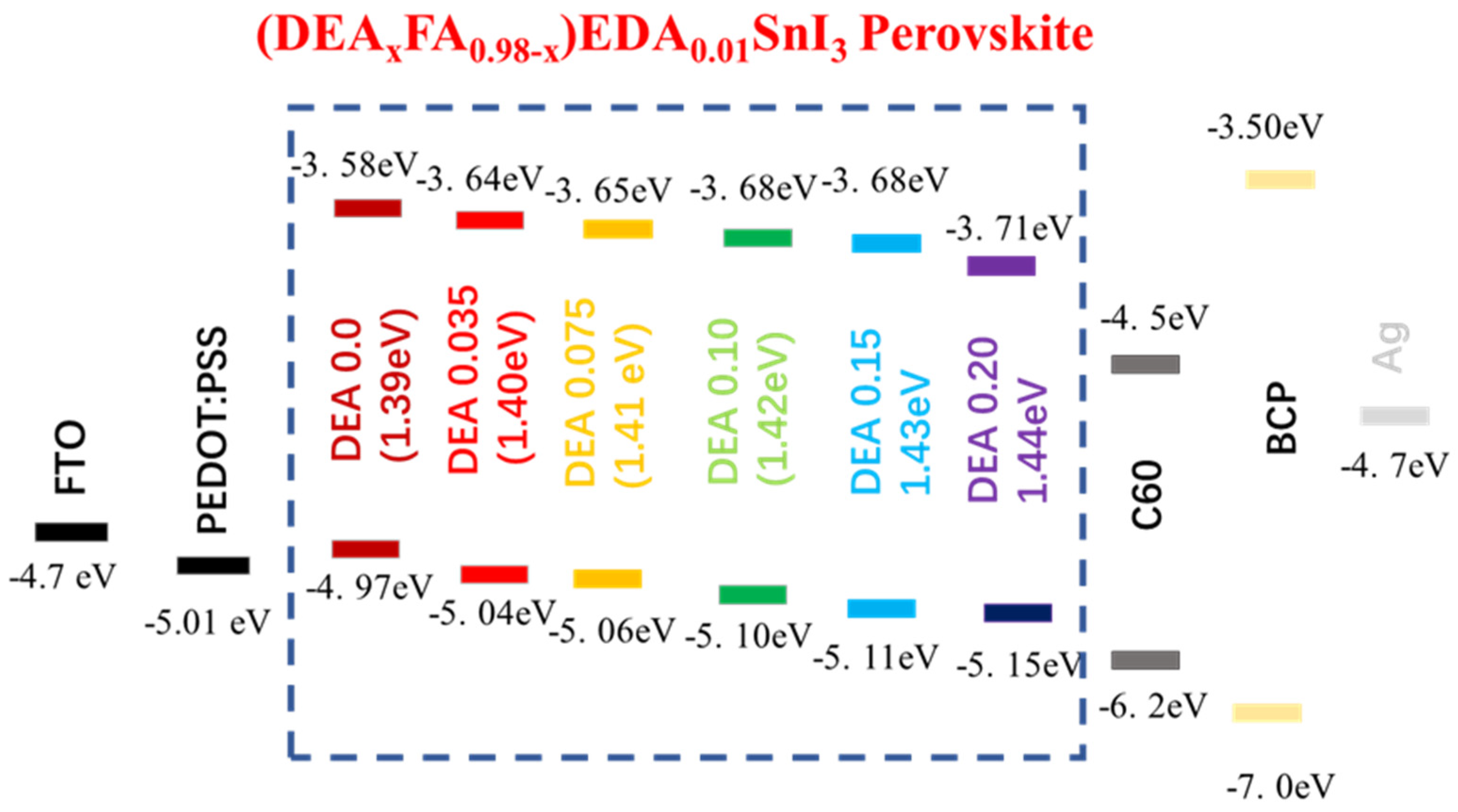
- Zhang, Z.; Kumar Baranwal, A.; Razey Sahamir, S.; Kapil, G.; Sanehira, Y.; Chen, M.; Nishimura, K.; Ding, C.; Liu, D.; Li, H.; et al. Large Grain Growth and Energy Alignment Optimization by Diethylammonium Iodide Substitution at A Site in Lead-Free Tin Halide Perovskite Solar Cells. Sol. RRL 2021, 5, 2100633. [Google Scholar] [CrossRef]
- Nakamura, T.; Yakumaru, S.; Truong, M.A.; Kim, K.; Liu, J.; Hu, S.; Otsuka, K.; Hashimoto, R.; Murdey, R.; Sasamori, T.; et al. Sn(IV)-free tin perovskite films realized by in situ Sn(0) nanoparticle treatment of the precursor solution. Nat. Commun. 2020, 11, 3008. [Google Scholar] [CrossRef]
- Kapil, G.; Bessho, T.; Maekawa, T.; Baranwal, A.K.; Zhang, Y.; Kamarudin, M.A.; Hirotani, D.; Shen, Q.; Segawa, H.; Hayase, S. Tin-Lead Perovskite Fabricated via Ethylenediamine Interlayer Guides to the Solar Cell Efficiency of 21.74%. Adv. Energy Mater. 2021, 11, 2101069. [Google Scholar] [CrossRef]
- Liao, M.; Yu, B.; Jin, Z.; Chen, W.; Zhu, Y.; Zhang, X.; Yao, W.; Duan, T.; Djerdj, I.; He, Z. Efficient and Stable FASnI3 Perovskite Solar Cells with Effective Interface Modulation by Low-Dimensional Perovskite Layer. ChemSusChem 2019, 12, 5007–5014. [Google Scholar] [CrossRef]
- Liu, X.; Wu, T.; Chen, J.-Y.; Meng, X.; He, X.; Noda, T.; Chen, H.; Yang, X.; Segawa, H.; Wang, Y.; et al. Templated growth of FASnI3 crystals for efficient tin perovskite solar cells. Energy Environ. Sci. 2020, 13, 2896–2902. [Google Scholar] [CrossRef]
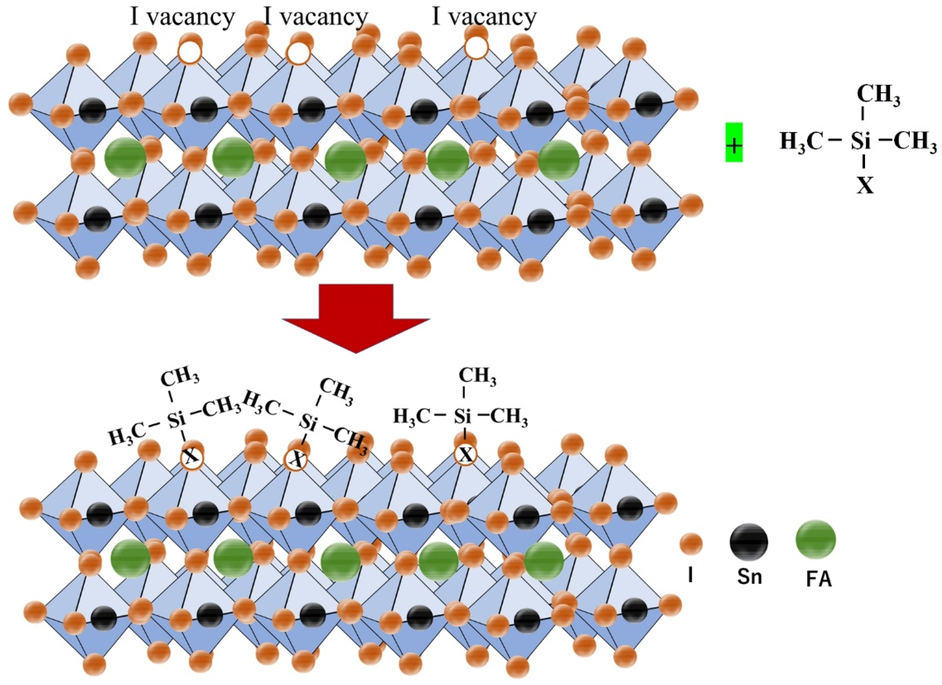
- Zhang, Z.; Wang, L.; Kumar Baranwal, A.; Razey Sahamir, S.; Kapil, G.; Sanehira, Y.; Akmal Kamarudin, M.; Nishimura, K.; Ding, C.; Liu, D.; et al. Enhanced efficiency and stability in Sn-based perovskite solar cells by trimethylsilyl halide surface passivation. J. Energy Chem. 2022, 71, 604–611. [Google Scholar] [CrossRef]
- Chowdhury, T.H.; Kayesh, M.E.; Lee, J.-J.; Matsushita, Y.; Kazaoui, S.; Islam, A. Post-Deposition Vapor Annealing Enables Fabrication of 1 cm2 Lead-Free Perovskite Solar Cells. Sol. RRL 2019, 3, 1900245. [Google Scholar] [CrossRef]
- Jokar, E.; Chien, C.-H.; Fathi, A.; Rameez, M.; Chang, Y.-H.; Diau, E.W.-G. Slow surface passivation and crystal relaxation with additives to improve device performance and durability for tin-based perovskite solar cells. Energy Environ. Sci. 2018, 11, 2353–2362. [Google Scholar] [CrossRef]
- Baranwal, A.K.; Nishimura, K.; Liu, D.; Kamarudin, M.A.; Kapil, G.; Saini, S.; Yabuki, T.; Iikubo, S.; Minemoto, T.; Yoshino, K.; et al. Relationship between Carrier Density and Precursor Solution Stirring for Lead-Free Tin Halide Perovskite Solar Cells Performance. ACS Appl. Energy Mater. 2022, 5, 4002–4007. [Google Scholar] [CrossRef]
- Chen, M.; Kapil, G.; Li, Y.; Kamarudin, M.A.; Baranwal, A.K.; Nishimura, K.; Sahamir, S.R.; Sanehira, Y.; Li, H.; Ding, C.; et al. Large synergy effects of doping, a site substitution, and surface passivation in wide bandgap Pb-free ASnI2Br perovskite solar cells on efficiency and stability enhancement. J. Power Sources 2022, 520, 230848. [Google Scholar] [CrossRef]
- Jokar, E.; Hou, P.; Bhosale, S.S.; Chuang, H.; Narra, S.; Wei-Guang Diau, E. Mixing of Azetidinium in Formamidinium Tin Triiodide Perovskite Solar Cells for Enhanced Photovoltaic Performance and High Stability in Air. ChemSusChem 2021, 14, 4415–4421. [Google Scholar] [CrossRef] [PubMed]
- Chen, M.; Kamarudin, M.A.; Baranwal, A.K.; Kapil, G.; Ripolles, T.S.; Nishimura, K.; Hirotani, D.; Sahamir, S.R.; Zhang, Z.; Ding, C.; et al. High-Efficiency Lead-Free Wide Band Gap Perovskite Solar Cells via Guanidinium Bromide Incorporation. ACS Appl. Energy Mater. 2021, 4, 5615–5624. [Google Scholar] [CrossRef]
- Wan, Z.; Ren, S.; Lai, H.; Jiang, Y.; Wu, X.; Luo, J.; Wang, Y.; He, R.; Chen, Q.; Hao, X.; et al. Suppression of Nonradiative Recombination by Vacuum-Assisted Process for Efficient Lead-Free Tin Perovskite Solar Cells. Adv. Mater. Interfaces 2021, 8, 2100135. [Google Scholar] [CrossRef]
- Li, B.; Di, H.; Chang, B.; Yin, R.; Fu, L.; Zhang, Y.; Yin, L. Efficient Passivation Strategy on Sn Related Defects for High Performance All-Inorganic CsSnI3 Perovskite Solar Cells. Adv. Funct. Mater. 2021, 31, 2007447. [Google Scholar] [CrossRef]
- Saidaminov, M.I.; Spanopoulos, I.; Abed, J.; Ke, W.; Wicks, J.; Kanatzidis, M.G.; Sargent, E.H. Conventional Solvent Oxidizes Sn(II) in Perovskite Inks. ACS Energy Lett. 2020, 5, 1153–1155. [Google Scholar] [CrossRef] [Green Version]
- Di Girolamo, D.; Pascual, J.; Aldamasy, M.H.; Iqbal, Z.; Li, G.; Radicchi, E.; Li, M.; Turren-Cruz, S.-H.; Nasti, G.; Dallmann, A.; et al. Solvents for Processing Stable Tin Halide Perovskites. ACS Energy Lett. 2021, 6, 959–968. [Google Scholar] [CrossRef]
- Nasti, G.; Aldamasy, M.H.; Flatken, M.A.; Musto, P.; Matczak, P.; Dallmann, A.; Hoell, A.; Musiienko, A.; Hempel, H.; Aktas, E.; et al. Pyridine Controlled Tin Perovskite Crystallization. ACS Energy Lett. 2022, 7, 3197–3203. [Google Scholar] [CrossRef] [PubMed]
- Cao, X.; Li, J.; Dong, H.; Li, P.; Fan, Q.; Xu, R.; Li, H.; Zhou, G.; Wu, Z. Stability Improvement of Tin-Based Halide Perovskite by Precursor-Solution Regulation with Dual-Functional Reagents. Adv. Funct. Mater. 2021, 31, 2104344. [Google Scholar] [CrossRef]
- Shahbazi, S.; Li, M.-Y.; Fathi, A.; Diau, E.W.-G. Realizing a Cosolvent System for Stable Tin-Based Perovskite Solar Cells Using a Two-Step Deposition Approach. ACS Energy Lett. 2020, 5, 2508–2511. [Google Scholar] [CrossRef]
- Ito, N.; Kamarudin, M.A.; Hirotani, D.; Zhang, Y.; Shen, Q.; Ogomi, Y.; Iikubo, S.; Minemoto, T.; Yoshino, K.; Hayase, S. Mixed Sn–Ge Perovskite for Enhanced Perovskite Solar Cell Performance in Air. J. Phys. Chem. Lett. 2018, 9, 1682–1688. [Google Scholar] [CrossRef]
- Ng, C.H.; Nishimura, K.; Ito, N.; Hamada, K.; Hirotani, D.; Wang, Z.; Yang, F.; Likubo, S.; Shen, Q.; Yoshino, K.; et al. Role of GeI2 and SnF2 additives for SnGe perovskite solar cells. Nano Energy 2019, 58, 130–137. [Google Scholar] [CrossRef]
- Wang, C.; Gu, F.; Zhao, Z.; Rao, H.; Qiu, Y.; Cai, Z.; Zhan, G.; Li, X.; Sun, B.; Yu, X.; et al. Self-Repairing Tin-Based Perovskite Solar Cells with a Breakthrough Efficiency Over 11%. Adv. Mater. 2020, 32, 1907623. [Google Scholar] [CrossRef]
- Zhang, J.; Bai, D.; Jin, Z.; Bian, H.; Wang, K.; Sun, J.; Wang, Q.; Liu, S. 3D-2D-0D Interface Profiling for Record Efficiency All-Inorganic CsPbBrI2 Perovskite Solar Cells with Superior Stability. Adv. Energy Mater. 2018, 8, 1703246. [Google Scholar] [CrossRef]
- Tsarev, S.; Boldyreva, A.G.; Luchkin, S.Y.; Elshobaki, M.; Afanasov, M.I.; Stevenson, K.J.; Troshin, P.A. Hydrazinium-assisted stabilization of methylammonium tin iodide for lead-free perovskite solar cells. J. Mater. Chem. A 2018, 6, 21389. [Google Scholar] [CrossRef]
- Song, T.-B.; Yokoyama, T.; Stoumpos, C.C.; Logsdon, J.; Cao, D.H.; Wasielewski, M.R.; Aramaki, S.; Kanatzidis, M.G. Importance of Reducing Vapor Atmosphere in the Fabrication of Tin-Based Perovskite Solar Cells. J. Am. Chem. Soc. 2017, 139, 836. [Google Scholar] [CrossRef]
- Li, P.; Dong, H.; Xu, J.; Chen, J.; Jiao, B.; Hou, X.; Li, J.; Wu, Z. Ligand Orientation-Induced Lattice Robustness for Highly Efficient and Stable Tin_Based Perovskite Solatr Cells. ACS Energy Lett. 2020, 5, 2327. [Google Scholar] [CrossRef]
- Meng, X.Y.; Wang, Y.B.; Lin, J.B.; Liu, X.; He, X.; Barbaud, J.; Wu, T.H.; Noda, T.; Yang, X.D.; Han, L.Y. Surface-Controlled Oriented Growth of FASnI3 Crystals for Efficient Lead-free Perovskite Solar Cells. Joule 2020, 4, 902. [Google Scholar] [CrossRef]
- Wang, F.; Geng, W.; Zhou, Y.; Fang, H.H.; Tong, C.J.; Loi, M.A.; Liu, L.M.; Zhao, N. Phenylalkylamine Passivation of Organolead Halide Perovskites Enabling High-Efficiency and Air-stable Perovskite Solar Cells. Adv. Mater. 2016, 28, 9986. [Google Scholar] [CrossRef] [PubMed]
- Alanazi, A.Q.; Almalki, M.H.; Mishra, A.; Kubicki, D.J.; Wang, Z.W.; Merten, L.; Eickemeyer, F.T.; Zhang, H.; Ren, D.; Alyamani, A.Y.; et al. Benzylammonium-Mediated Formamidinium Lead Iodide Perovskite Phase Stabilization For Photovoltaica. Adv. Funct. Mater. 2021, 31, 2101163. [Google Scholar] [CrossRef]
- Sanchez-Diaz, J.; Sánchez, R.S.; Masi, S.; Kreĉmarová, M.; Alvarez, A.O.; Barea, E.M.; Rodriguez-Romero, J.; Chirvony, V.S.; Sánchez-Royo, J.F.; Martinez-Pastor, J.P.; et al. Tin perovskite solar cells with >1,300 h of operational stability in N2 through a synergistic chemical engineering approach. Joule 2022, 6, 861–883. [Google Scholar] [CrossRef] [PubMed]
- Liu, C.; Tu, J.; Hu, X.; Huang, Z.; Meng, X.; Yang, J.; Duan, X.; Tan, L.; Li, Z.; Chen, Y. Enhanced Hole Transportation for Inverted Tin-Based Perovskite Solar Cells with High Performance and Stability. Adv. Funct. Mater. 2019, 29, 1808059. [Google Scholar] [CrossRef]
- Yu, B.-B.; Xu, L.; Liao, M.; Wu, Y.; Liu, F.; He, Z.; Ding, J.; Chen, W.; Tu, B.; Lin, Y.; et al. Synergy Effect of Both 2,2,2-Trifluoroethylamine Hydrochloride and SnF2 for Highly Stable FASnI3−xClx Perovskite Solar Cells. Sol. RRL 2019, 3, 1800290. [Google Scholar] [CrossRef]
- Meng, X.; Lin, J.; Liu, X.; He, X.; Wang, Y.; Noda, T.; Wu, T.; Yang, X.; Han, L. Highly Stable and Efficient FASnI3-Based Perovskite Solar Cells by Introducing Hydrogen Bonding. Adv. Mater. 2019, 31, 1903721. [Google Scholar] [CrossRef]
- Mahmoudi, T.; Kohan, M.; Rho, W.; Wang, Y.; Im, Y.H.; Hahn, Y. Tin-Based Perovskite Solar Cells Over 13% with Inclusion of N-Doped Graphene Oxide in Active, Hole-Transport and Interfacial Layers. Adv. Energy Mater. 2022, 12, 2201977. [Google Scholar] [CrossRef]
- Chen, J.; Tian, C.; Sun, C.; Yang, P.; Feng, W.; Zheng, L.; Yang, L.; Hou, E.; Luo, J.; Xie, L.; et al. Chlorofullerene C60Cl6 Enables Efficient and Stable Tin-Based Perovskite Solar Cells. Energy Environ. Mater. 2022, e12529. [Google Scholar] [CrossRef]
- Yu, B.; Liao, M.; Zhu, Y.; Zhang, X.; Du, Z.; Jin, Z.; Liu, D.; Wang, Y.; Gatti, T.; Ageev, O.; et al. Oriented Crystallization of Mixed-Cation Tin Halides for Highly Efficient and Stable Lead-Free Perovskite Solar Cells. Adv. Funct. Mater. 2020, 30, 2002230. [Google Scholar] [CrossRef]
- Ito, S.; Baranwal, A.K.; Kanda, H.; Shibayama, N.; Masutani, H.; Peiris, T.A.N.; Kanaya, S.; Segawa, H.; Miyasaka, T. Thermal Degradation Analysis of Sealed Perovskite Solar Cell with Porous Carbon Electrode at 100 °C for 7000 h. Energy Technol. 2018, 7, 245–252. [Google Scholar] [CrossRef]
- Rameez, M.; Shahbazi, S.; Raghunath, P.; Lin, M.C.; Hung, C.H.; Diau, E.W.-G. Development of Novel Mixed Halide/Superhalide Tin-Based Perovskites for Mesoscopic Carbon-Based Solar Cells. J. Phys. Chem. Lett. 2020, 11, 2443–2448. [Google Scholar] [CrossRef] [PubMed]
- Ban, H.; Zhang, T.; Gong, X.; Sun, Q.; Zhang, X.-L.; Pootrakulchote, N.; Shen, Y.; Wang, M. Fully Inorganic CsSnI3 Mesoporous Perovskite Solar Cells with High Efficiency and Stability via Coadditive Engineering. Sol. RRL 2021, 5, 2100069. [Google Scholar] [CrossRef]
- Chen, Y.; Cao, K.; Cheng, Y.; Shen, H.; Du, C.; Wang, Q.; Chen, C.; Cui, H.; Lan, T.; Liu, L.; et al. p-Type Dopants As Dual Function Interfacial Layer for Efficient and Stable Tin Perovskite Solar Cells. Sol. RRL 2021, 5, 2100068. [Google Scholar] [CrossRef]
- Tian, C.; Sun, C.; Chen, J.; Song, P.; Hou, E.; Xu, P.; Liang, Y.; Yang, P.; Luo, J.; Xie, L.; et al. Fullerene Derivative with Flexible Alkyl Chain for Efficient Tin-Based Perovskite Solar Cells. Nanomaterials 2022, 12, 532. [Google Scholar] [CrossRef]
- Chen, M.; Kapil, G.; Wang, L.; Razey Sahamir, S.; Baranwal, A.K.; Nishimura, K.; Sanehira, Y.; Zhang, Z.; Akmal Kamarudin, M.; Shen, Q.; et al. High performance wide bandgap Lead-free perovskite solar cells by monolayer engineering. Chem. Eng. J. 2022, 436, 135196. [Google Scholar] [CrossRef]
- Rao, L.; Meng, X.; Xiao, S.; Xing, Z.; Fu, Q.; Wang, H.; Gong, C.; Hu, T.; Hu, X.; Guo, R.; et al. Wearable Tin-Based Perovskite Solar Cells Achieved by a Crystallographic Size Effect. Angew. Chemie Int. Ed. 2021, 60, 14693–14700. [Google Scholar] [CrossRef]
- Liu, X.; Wu, T.; Zhang, C.; Zhang, Y.; Segawa, H.; Han, L. Interface Energy-Level Management toward Efficient Tin Perovskite Solar Cells with Hole-Transport-Layer-Free Structure. Adv. Funct. Mater. 2021, 31, 2106560. [Google Scholar] [CrossRef]
- Wijesekara, A.; Walker, M.; Han, Y.; Walker, D.; Huband, S.; Hatton, R.A. Enhanced Stability of Tin Halide Perovskite Photovoltaics Using a Bathocuproine—Copper Top Electrode. Adv. Energy Mater. 2021, 11, 2102766. [Google Scholar] [CrossRef]
- Zhang, X.; Wang, S.; Zhu, W.; Cao, Z.; Wang, A.; Hao, F. The Voltage Loss in Tin Halide Perovskite Solar Cells: Origins and Perspectives. Adv. Funct. Mater. 2022, 32, 2108832. [Google Scholar] [CrossRef]
- Wu, T.; Liu, X.; Luo, X.; Segawa, H.; Tong, G.; Zhang, Y.; Ono, L.K.; Qi, Y.; Han, L. Heterogeneous FASnI3 Absorber with Enhanced Electric Field for High-Performance Lead-Free Perovskite Solar Cells. Nano-Micro Lett. 2022, 14, 99. [Google Scholar] [CrossRef] [PubMed]
- Wang, C.; Zhang, Y.; Gu, F.; Zhao, Z.; Li, H.; Jiang, H.; Bian, Z.; Liu, Z. Illumination Durability and High-Efficiency Sn-Based Perovskite Solar Cell under Coordinated Control of Phenylhydrazine and Halogen Ions. Matter 2021, 4, 709–721. [Google Scholar] [CrossRef]
- Chen, Y.; Wang, K.; Qi, H.; Zhang, Y.; Wang, T.; Tong, Y.; Wang, H. Mitigating Voc Loss in Tin Perovskite Solar Cells via Simultaneous Suppression of Bulk and Interface Nonradiative Recombination. ACS Appl. Mater. Interfaces 2022, 14, 36. [Google Scholar] [CrossRef]
- Kamarudin, M.A.; Sahamir, S.R.; Nishimura, K.; Iikubo, S.; Yoshino, K.; Minemoto, T.; Shen, Q.; Hayase, S. Suppression of Defect and Trap Density through Dimethylammonium-Substituted Tin Perovskite Solar Cells. ACS Mater. Lett. 2022, 4, 1855–1862. [Google Scholar] [CrossRef]
- Meng, X.; Wu, T.; Liu, X.; He, X.; Noda, T.; Wang, Y.; Segawa, H.; Han, L. Highly Reproducible and Efficient FASnI3 Perovskite Solar Cells Fabricated with Volatilizable Reducing Solvent. J. Phys. Chem. Lett. 2020, 11, 2965–2971. [Google Scholar] [CrossRef]
- Ye, T.; Wang, X.; Wang, K.; Ma, S.; Yang, D.; Hou, Y.; Yoon, J.; Wang, K.; Priya, S. Localized Electron Density Engineering for Stabilized B-γ CsSnI3-Based Perovskite Solar Cells with Efficiencies > 10%. ACS Energy Lett. 2021, 6, 1480–1489. [Google Scholar] [CrossRef]
- Bilotti, E.; Fenwick, O.; Schroeder, B.C.; Baxendale, M.; Taroni-Junior, P.; Degousée, T.; Liu, Z. 6.14 Organic Thermoelectric Composites Materials. In Comprehensive Composite Materials II; Elsevier: Amsterdam, The Netherlands, 2018; Volume 6, pp. 408–430. ISBN 978-0-08100-533-0. [Google Scholar]
- Haque, M.A.; Nugraha, M.I.; Paleti, S.H.K.; Baran, D. Role of Compositional Tuning on Thermoelectric Parameters of Hybrid Halide Perovskites. J. Phys. Chem. C 2019, 123, 14928–14933. [Google Scholar] [CrossRef]
- Schierning, G. Bring on the Heat. Nat. Energy 2018, 3, 92–93. [Google Scholar] [CrossRef]
- Saini, S.; Baranwal, A.K.; Yabuki, T.; Hayase, S.; Miyazaki, K. Growth of halide perovskites thin films for thermoelectric applications. MRS Adv. 2019, 4, 1719–1725. [Google Scholar] [CrossRef]
- Saini, S.; Baranwal, A.K.; Yabuki, T.; Hayase, S.; Miyazaki, K. Unileg Thermoelectric Module Comprised by Coated Halide-Perovskite Thin Film. J. Heat Transfer 2020, 142, 074502. [Google Scholar] [CrossRef]
- Tang, W.; Liu, T.; Fenwick, O. High thermoelectric performance based on CsSnI3 thin films with improved stability. J. Mater. Chem. A 2022, 10, 7020–7028. [Google Scholar] [CrossRef]
- Qian, F.; Hu, M.; Gong, J.; Ge, C.; Zhou, Y.; Guo, J.; Chen, M.; Ge, Z.; Padture, N.P.; Zhou, Y.; et al. Enhanced Thermoelectric Performance in Lead-Free Inorganic CsSn1–xGexI3 Perovskite Semiconductors. J. Phys. Chem. C 2020, 124, 11749–11753. [Google Scholar] [CrossRef]
- Xie, H.; Hao, S.; Bao, J.; Slade, T.J.; Snyder, G.J.; Wolverton, C.; Kanatzidis, M.G. All-Inorganic Halide Perovskites as Potential Thermoelectric Materials: Dynamic Cation off-Centering Induces Ultralow Thermal Conductivity. J. Am. Chem. Soc. 2020, 142, 9553–9563. [Google Scholar] [CrossRef] [PubMed]
- Liu, T.; Zhao, X.; Li, J.; Liu, Z.; Liscio, F.; Milita, S.; Schroeder, B.C.; Fenwick, O. Enhanced control of self-doping in halide perovskites for improved thermoelectric performance. Nat. Commun. 2019, 10, 5750. [Google Scholar] [CrossRef] [Green Version]
- Baranwal, A.K.; Saini, S.; Yabuki, T.; Shen, Q.; Miyazaki, K.; Hayase, S. Formamidinium doped CsSnI 3 perovskite for thermoelectric applications. In Proceedings of the 81st JSAP Autumn Meeting, Online, 8–11 September 2020. [Google Scholar] [CrossRef]
- Chen, R.; Yan, Y.; Tang, J.; Zeng, H.; Yao, Q.; Chen, L.; Liang, Z. Efficient p-Type Doping of Tin Halide Perovskite via Sequential Diffusion for Thermoelectrics. Small Sci. 2022, 2, 2200004. [Google Scholar] [CrossRef]
- Zheng, L.; Zhu, T.; Li, Y.; Wu, H.; Yi, C.; Zhu, J.; Gong, X. Enhanced thermoelectric performance of F4-TCNQ doped FASnI3 thin films. J. Mater. Chem. A 2020, 8, 25431–25442. [Google Scholar] [CrossRef]
- Saini, S.; Baranwal, A.K.; Yabuki, T.; Hayase, S.; Miyazaki, K. Hybrid-Halide Perovskite Thin Film Growth for Thermoelectric Applications. J. Electron. Mater. 2020, 49, 2890–2894. [Google Scholar] [CrossRef]
- Saini, S.; Matsumoto, I.; Kishishita, S.; Baranwal, A.K.; Yabuki, T.; Hayase, S.; Miyazaki, K. Use of anti-solvent to enhance thermoelectric response of hybrid halide perovskite thin films. Jpn. J. Appl. Phys. 2022, 61, SE1019. [Google Scholar] [CrossRef]
- Cohen, B.-E.; Aharon, S.; Dymshits, A.; Etgar, L. Impact of Antisolvent Treatment on Carrier Density in Efficient Hole-Conductor-Free Perovskite-Based Solar Cells. J. Phys. Chem. C 2016, 120, 142–147. [Google Scholar] [CrossRef]
- Haque, M.A.; Hernandez, L.H.; Davaasuren, B.; Villalva, D.R.; Troughton, J.; Baran, D. Tuning the Thermoelectric Performance of Hybrid Tin Perovskites by Air Treatment. Adv. Energy Sustain. Res. 2020, 1, 2000033. [Google Scholar] [CrossRef]
- Lanzetta, L.; Webb, T.; Zibouche, N.; Liang, X.; Ding, D.; Min, G.; Westbrook, R.J.E.; Gaggio, B.; Macdonald, T.J.; Islam, M.S. Degradation mechanism of hybrid tin-based perovskite solar cells and the critical role of tin(IV) iodide. Nat. Comm. 2021, 12, 2853. [Google Scholar] [CrossRef] [PubMed]
- Stoumpos, C.C.; Malliakas, C.D.; Kanatzidis, M.G. Semiconducting Tin and Lead Iodide Perovskites with Organic Cations: Phase Transitions, High Mobilities, and Near-Infrared Photoluminescent Properties. Inorg. Chem. 2013, 52, 9019–9038. [Google Scholar] [CrossRef]
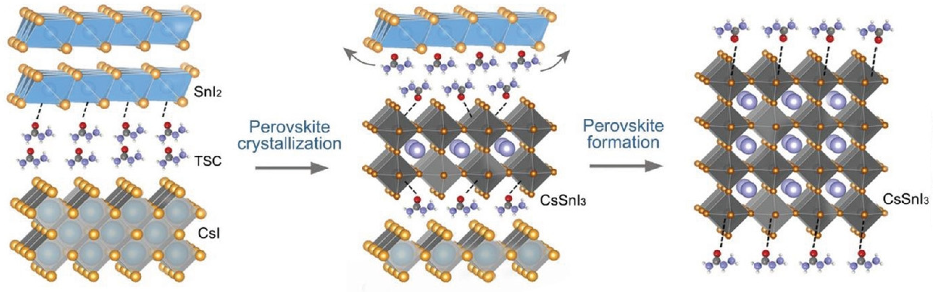
- Sebastia-Luna, P.; Pokharel, U.; Huisman, B.A.H.; Koster, L.J.A.; Palazon, F.; Bolink, H.J. Vacuum-Deposited Cesium Tin Iodide Thin Films with Tunable Thermoelectric Properties. ACS Appl. Energy Mater. 2022, 5, 10216–10223. [Google Scholar] [CrossRef] [PubMed]
- Ide, A.; Iikubo, S.; Yamamoto, K.; Shen, Q.; Yoshino, K.; Minemoto, T.; Hayase, S. Structural stability and optical properties of tin-based iodide perovskite. Jpn. J. Appl. Phys. 2022, 61, 031003. [Google Scholar] [CrossRef]
- Matsushita, S.; Sugawara, S.; Isobe, T.; Nakajima, A. Temperature Dependence of a Perovskite-Sensitized Solar Cell: A Sensitized “Thermal” Cell. ACS Appl. Energy Mater. 2019, 2, 13–18. [Google Scholar] [CrossRef]


| CsSnI3 | MASnI3 | FASnI3 | FASnI2Br | FASnIBr2 | |
|---|---|---|---|---|---|
| Tolerance factor | 0.82 | 0.93 | 0.99 | 1.00 | 1.01 |
| RCs + = 167 pm; RMA + = 216 pm; FA + = 253 pm; RSn2 + = 115 pm; RI− = 220 pm; RBr− = 196 pm [27] | |||||
| MASnI3 | MASnBr3 | |||||
|---|---|---|---|---|---|---|
| Bandgap/eV | Bandgap/eV | |||||
| Cubic | 0.83 | 0.17 | 0.11 | 1.12 | 0.19 | 0.14 |
| Tetragonal Parallel | 0.73 | 0.11 | 0.10 | 1.06 | 0.17 | 0.14 |
| Tetragonal Vertical | 0.93 | 0.15 | 0.14 | 1.36 | 0.25 | 0.19 |
| Orthorhombic | 1.08 | 0.19 | 0.18 | 1.53 | 0.22 | 0.23 |
| Sample | |||||
|---|---|---|---|---|---|
| α-CsSnCl3 | 0.140 | 0.741 | 0.272 | 0.088 | 0.149 |
| α-CsSnBr3 | 0.082 | 0.635 | 0.201 | 0.053 | 0.084 |
| α-CsSnI3 | 0.069 | 0.573 | 0.154 | 0.041 | 0.068 |
| Perovskite | Hole Mobility/cm2/V·s | Diffusion Length/nm | Charge Life Time τ [ns] | Acceptor Defect Density [1015/cm3] | Trap Density [1015/cm3] | Ref. |
|---|---|---|---|---|---|---|
| (Cs0.02(FA0.9DEA0.1)0.98)0.98EDA0.01I3-GeI2 | _ | _ | _ | _ | 9.55/SC | [49] |
| FASnI3-GeI2-EDABr2 | 2.97 × 10⁻² | _ | 37.83 | 5.76/M-S | 19.3/SC | [50] |
| FASnI3-FPEABr | _ | _ | 2.87 | _ | 3.32/SC | [20] |
| FASnI3-PEAI-trimethylthiourea | _ | _ | 123 | _ | [51] | |
| FA0.98EDA0.01SnI3 | _ | _ | _ | _ | 4.16/SC | [52] |
| (FAxEA1-x)0.98EDA0.01SnI3-GeI2 | 9.27 × 10⁻³ | 348 | 20.1 | 5.48/M-S | 29/SC | [53] |
| FA0.98EDA0.01SnI3/GeI2/FBZAI | _ | _ | 19.8 | 6.76/M-S | _ | [54] |
| FASnI3/PEAI/GuaSCN | 9 × 10⁻⁴ | _ | _ | _ | [55] | |
| (Cs0.02(FA0.9DEA0.1)0.98)EDA0.01I3)GeI2/ACAC/EDA | _ | _ | 12.85 | _ | 9.1 /SC | [56] |
| FASnI3-PEABr/NH4SCN/GAA | _ | _ | 3.60 | _ | 9.8 /SC | [57] |
| CsSnI2.4Br0.6-dimethyl ketoxime | _ | _ | 15.4 | _ | 12.4/SC | [58] |
| FA0.8GA0.2SnI3-PHSCN | _ | 10.8 | [59] | |||
| (PEA)0.15FA0.85SnI2.55Br0.45 | _ | 290 | [60] |
| Solar Cell Structure | Efficiency [%] | Jsc [mA/cm2] | Voc [V] | FF | Voc Loss [V] | Ref. |
|---|---|---|---|---|---|---|
| ITO/PEDOT:PSS/(FPEA)0.1FA0.9SnI2.9Br0.1/ICBA/BCP/Al | 14.81 | 24.91 | 0.84 | 0.71 | 0.59 | [20] |
| ITO/PEDOT:PSS/(PEA)0.15FA0.85SnI2.55Br0.45/ICBA/BCP/Ag | 14.63 | 20.6 | 0.91 | 0.77 | 0.49 | [60] |
| ITO/PEDOT:PSS/FASnI3-PEAI-trimethylthiourea/N methyl thiourea/ICBA/BCP/Ag | 14.38 | 20.3 | 0.92 | 0.77 | 0.48 | [51] |
| ITO/PEDOT:PSS/FASnI3-GeI2-EDABr2 | 14.23 | 22.49 | 0.817 | 0.774 | 0.563 | [47,50] |
| ITO/PEDOT:PSS/FA0.98EDA0.01SnI3/C60-BPY/C60/BCP/Ag | 14.14 | 23.14 | 0.82 | 0.72 | 0.58 | [52] |
| FTO/P-SnOx/(Cs0.02(FA0.9DEA0.1)0.98)0.98EDA0.01I3-GeI2/T-SnOx/PCBM:ICBA/C60/BCP/Ag | 14.09 | 24.09 | 0.78 | 0.75 | 0.62 | [49] |
| ITO/PEDOT:PSS/FA0.98EDA0.01SnI3/GeI2/FBZAI/C60/BCP/Cu | 13.85 | 22.87 | 0.78 | 0.78 | 0.61 | [54] |
| ITO/PEDOT:PSS/FA0.99EDA0.005SnI3/<PMMA>/C60/BCP/Ag | 13.82 | 22.74 | 0.85 | 0.72 | 0.56 | [132] |
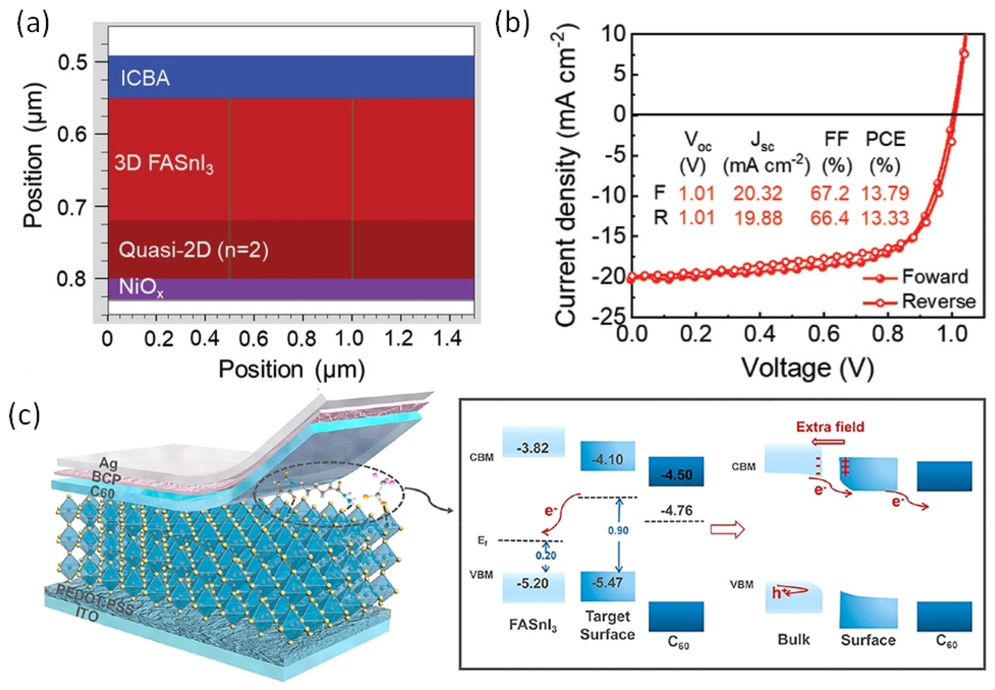
| ITO/NiOx/FASnI3/PEAI/GuaSCN/ICBA/BCP/Ag | 13.79 | 20.32 | 1.01 | 0.67 | 0.39 | [55] |
| ITO/PEDOT:PSS/FASnI3-PEABr/NH4SCN/GAA/ICBA/BCP/Ag | 13.70 | 19.66 | 0.93 | 0.75 | 0.47 | [57] |
| ITO/PEDOT:PSS/FASnI3/EDADI/Sn<6-MaleiMidocaproic Acid Hydrazide, trifluoroacetic Acid>/BCP/C60/Ag | 13.64 | 23.08 | 0.803 | 0.73 | 0.567 | [83] |
| ITO/PEDOT:PSS/FA0.8GA0.2SnI3-(PHSCN)/C60/BCP/Ag | 13.50 | 21.9 | 0.81 | 0.76 | 0.59 | [59] |
| ITO/PEDOT:PSS/FASnI2.85Br0.1Cl0.05/C60/BCP/Ag | 13.40 | 23.02 | 0.81 | 0.72 | 0.59 | [133] |
| ITO/PEDOT:PSS/PEA0.15FA0.85SnI3/C60Cl6/C60/BCP/Ag | 13.30 | 20.31 | 0.86 | 0.76 | 0.54 | [120] |
| FTO/PEDOT:PSS-N0.12GO/Al2O3-N0.12GO/FA0.8MA0.2SnI3:N0.12GO//BCP/Au | 13.26 | 21.21 | 0.961 | 0.651 | 0.42 | [119] |
| FTO/PEDOT:PSS/(FAxEA1-x)0.98EDA0.01SnI3-GeI2/C60/BCP/Ag | 13.24 | 20.32 | 0.84 | 0.78 | 0.56 | [53] |
| FTO/PEDOT:PSS/(Cs0.02(FA0.9DEA0.1)0.98)EDA0.01I3)GeI2/<ACAC/EDA>/C60/BCP/Ag | 13.00 | 22.70 | 0.79 | 0.72 | 0.65 | [56] |
| FTO/PEDOT:PSS/FA0.98EDA0.01SnI3/GeI2/<Me3SiBr>/C60/BCP/Ag | 12.22 | 24.11 | 0.70 | 0.72 | 0.72 | [91] |
| ITO/PEDOT:PSS/FASnI3-TG/C60/BCP/Ag | 11.78 | 22.82 | 0.73 | 0.72 | 0.67 | [90] |
| ITO/PEDOT:PSS/FA0.75MA0.25SnI3/TM-DHP/<EDA>/PCBM/C60/BCP/Ag | 11.50 | 22 | 0.76 | 0.69 | 0.60 | [87] |
| ITO/PEDOT:PSS/FASnI3/PHCl/C60/BCP/Ag | 11.40 | 23.5 | 0.76 | 0.64 | 0.64 | [107] |
| FTO/PEDOT:PSS/FA0.98EDA0.010SnI3/GeI2-<EDA vapor>/BCP/Ag | 11.29 | 24.05 | 0.66 | 0.71 | 0.74 | [85] |
| ITO/PEDOT:PSS/FAPEASnI3Br/EABr/PCBM/BCP/Ag | 10.80 | 18.74 | 0.83 | 0.69 | 0.65 | [134] |
| FTO/PEDOT:PSS/FA0.98DMAxEDA0.01SnI3-<EDA>/C60/BCP/Ag | 10.78 | 24.30 | 0.63 | 0.78 | 0.80 | [135] |
| FTO/PEDOT:PSS/FASnI3/Dipl/NaBH4/C60/BCP/Ag | 10.61 | 22.13 | 0.66 | 0.73 | 0.72 | [115] |
| FTO/PEDOT:PSS/FA0.8GA0.2SnI3/C60/BCP/Ag | 10.60 | 21.10 | 0.645 | 0.76 | 0.755 | [80] |
| ITO/PEDOT:PSS/FA0.95MA0.05EDA0.01SnI3/PCBM/BCP | 10.58 | 23.16 | 0.68 | 0.67 | 0.71 | [129] |
| PET/ITO/NiOx/FASn0.9Ge0.2I3/4(AMP)I2/PCBM/BCP/Ag | 10.43 | 21.3 | 0.69 | 0.71 | 0.71 | [77] |
| ITO/PEDOT:PSS/FASnI3/LFA/C60/BCP/Ag | 10.37 | 22.25 | 0.63 | 0.74 | 0.77 | [136] |
| ITO/PEDOT:PSS/FA0.75MA0.25SnI3/PEAI/C60/BCP/Ag | 10.30 | 21.62 | 0.63 | 0.76 | 0.74 | [98] |
| FTO/PEDOT:PSS/(EA0.1FA0.9)0.98EDA0.010SnI3/GeI2-DMF as stirring solvent/BCP/Ag | 10.28 | 23.32 | 0.59 | 0.75 | 0.81 | [94] |
| FTO/PEDOT:PSS/(DEAxFA1–x)0.98EDA0.01SnI3/GeI2/<EDA>/C60/BCP/Ag | 10.28 | 21.69 | 0.67 | 0.71 | 0.75 | [86] |
| ITO/PEDOT:PSS/PEA0.15EA0.15FA0.70SnI2.7Br0.3/PCBM/BCP/Ag | 10.12 | 21.12 | 0.68 | 0.70 | 0.80 | [81] |
| ITO/FA0.95MA0.05EDA0.01SnI3/PCBM/BCP | 10.11 | 22.03 | 0.67 | 0.67 | 0.72 | [129] |
| ITO/PEDOT:PSS/CsSnI3-PTM/ICBA/BCP/Ag | 10.10 | 21.81 | 0.64 | 0.72 | 0.67 | [137] |
| ITO/PEDOT:PSS/FASnI3/2F-PEAI/EDAI2/<DMF-AP> solvent/C60/BCP/Ag | 10.03 | 22.02 | 0.65 | 0.71 | 0.75 | [103] |
| Sn-PVK | σ [S/cm] | S [µV/K] | Power Factor [µW/m·K2] | K [W/m·K] | ZT | Measurement Temp | Ref. |
|---|---|---|---|---|---|---|---|
| CsSnI3 | 124 | +115 | 164 | 0.36 | 0.137 | 27 °C | [141] |
| MASnI3 | 3.56 | +66.03 | 1.55 | - | - | 50 °C | [150] |
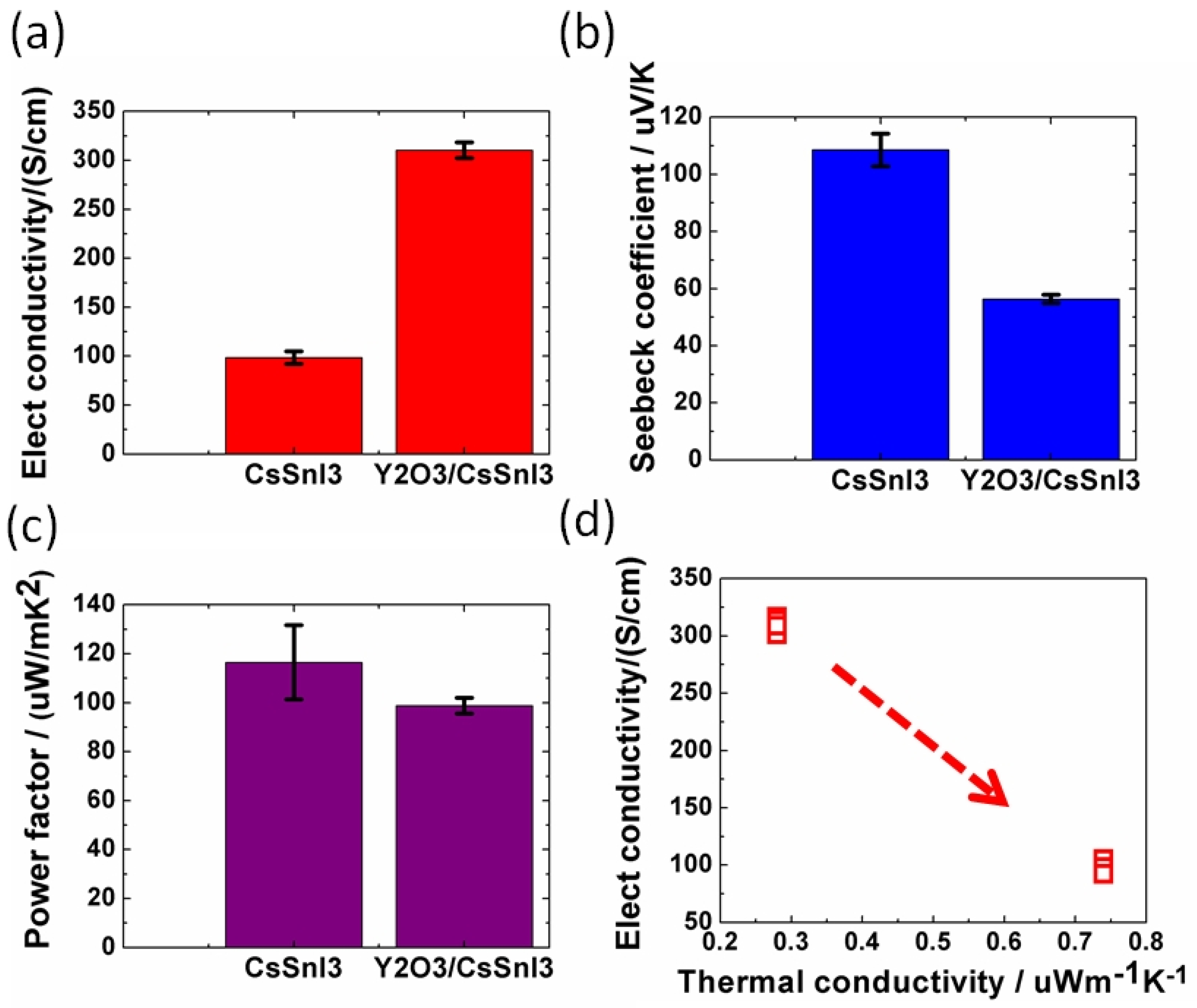
| CsSnI3/Y2O3 | 316.67 | +56.08 | 99.60 | 0.28 | 0.11 | 27 °C | [76] |
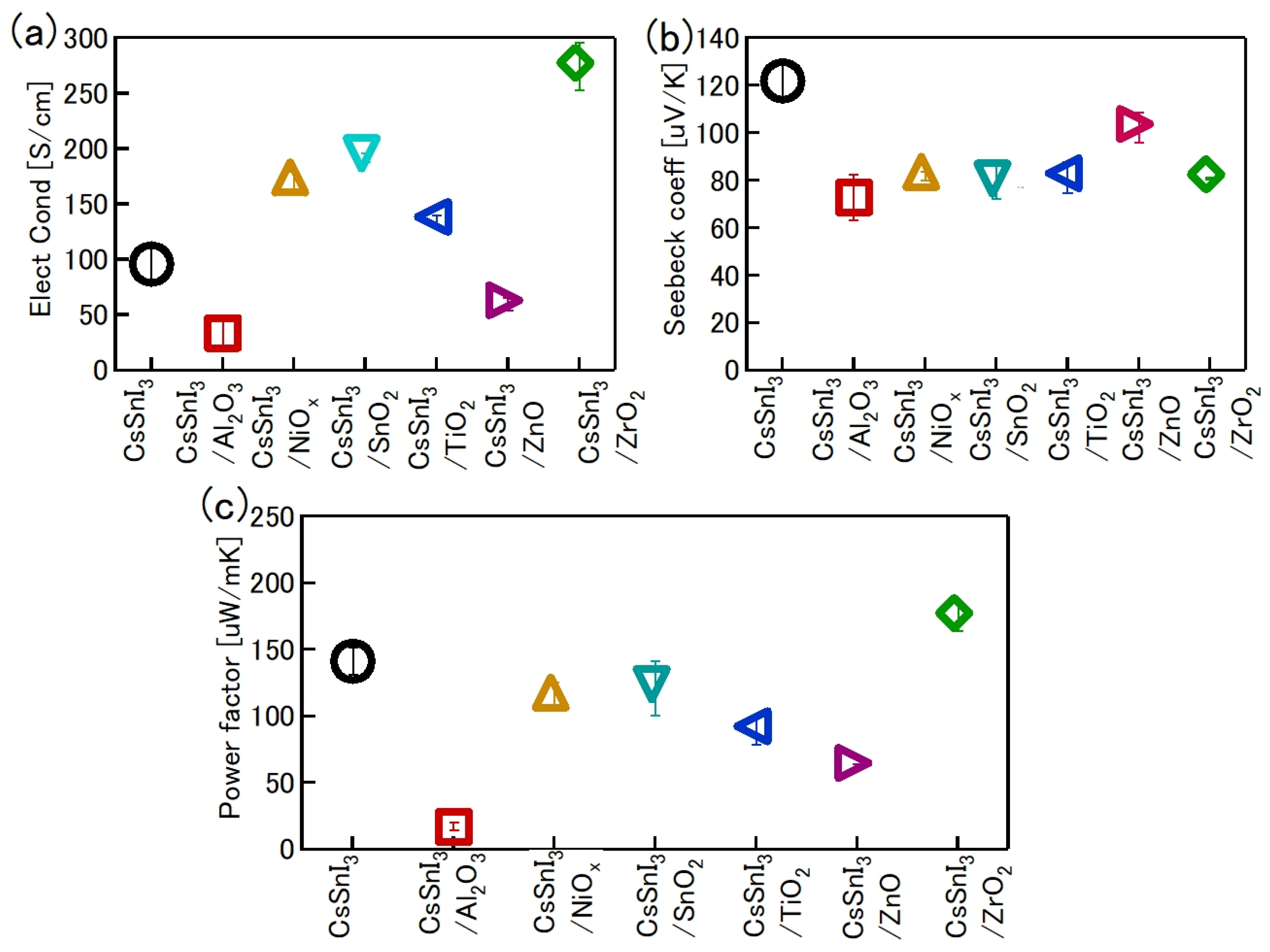
| CsSnI3 | 106 | +117 | 145.10 | - | - | 27 °C | [38] |
| CsSnI3 | 115 | +113.68 | 148.61 | - | - | 27 °C | [40] |
| CsSnI3/Al2O3 | 50 | +62.63 | 19.61 | - | - | 27 °C | [40] |
| CsSnI3/NiOx | 180 | +84.80 | 127.25 | - | - | 27 °C | [40] |
| CsSnI3/TiO2 | 130 | +81.42 | 100.94 | - | - | 27 °C | [40] |
| CsSnI3/ZnO | 55 | +107.58 | 63.65 | - | - | 27 °C | [40] |
| CsSnI3/ZrO2 | 288 | +80.49 | 186.58 | - | - | 27 °C | [40] |
| MASnI3 | 1.64 | +1.01 | 1.55 | - | - | 46 °C | [151] |
| CsSnI3 film | 50 | +118 | - | 0.69 | 0.003 | [156] | |
| Cs2SnI6 film | 0.128 ± 0.007 | −255 ± 18 | - | 0.30 | 0.0011 | 100 °C | [156] |
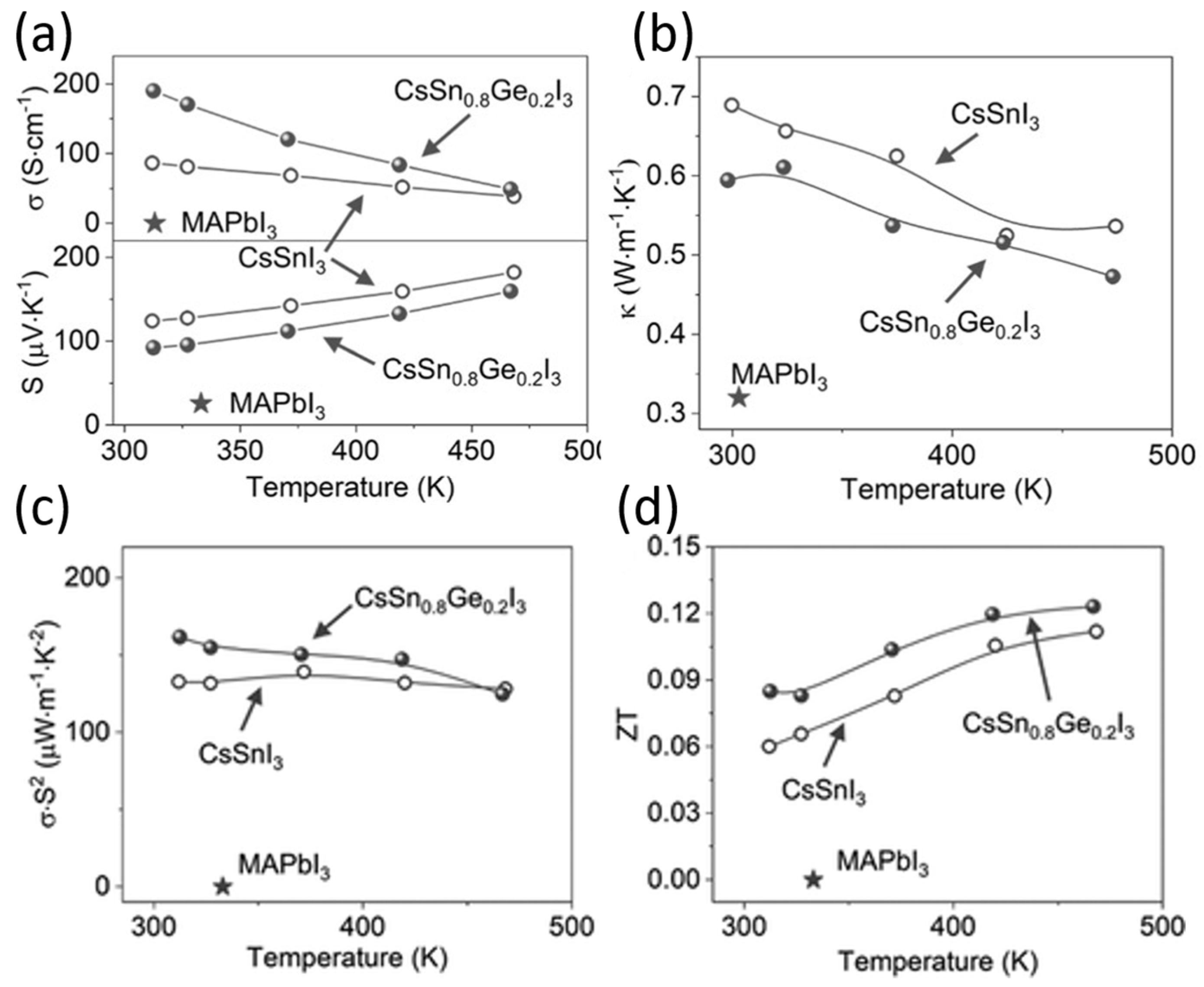
| CsSn0.8Ge0.2I3 bulk crystal | 190.1 | +92.2 | 162 | 0.60 | 0.088 | 27 °C | [144] |
| CsSnI3 film | 50 | 110 | 60 | 0.28 | 0.08 | - | [143] |
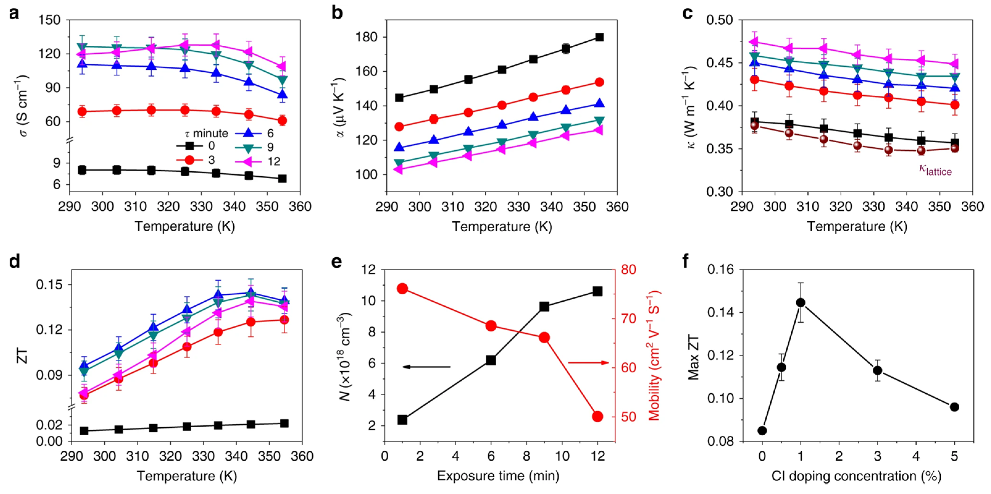
| CsSnI3−xClx film | 105 | 115 | - | 0.38 | 0.14 | 345 K | [146] |
| FASnI3/F4ATCNQ | 18 | 175 | 53 | 0.296 | 0.05 | 27 °C | [148] |
| MASnI3 | 22 | 78 | - | - | - | 27 °C | [153] |
| MAPb0.75Sn0.25I3 | 1.2 | 114 | - | - | - | 27 °C | [153] |
| FASnI3 | 2.81 | 213 | 12.74 | 0.141 | 0.03 | - | [149] |
| FASnI3-F4TCNQ | 13.65 | 310 | 130 | 0.212 | 0.19 | 27 °C | [149] |
| CsSnI3 ingot | 65 | 133 | 115 | 0.37 | 0.15 | 550 K | [145] |
Publisher’s Note: MDPI stays neutral with regard to jurisdictional claims in published maps and institutional affiliations. |
© 2022 by the authors. Licensee MDPI, Basel, Switzerland. This article is an open access article distributed under the terms and conditions of the Creative Commons Attribution (CC BY) license (https://creativecommons.org/licenses/by/4.0/).
Share and Cite
Baranwal, A.K.; Hayase, S. Recent Advancements in Tin Halide Perovskite-Based Solar Cells and Thermoelectric Devices. Nanomaterials 2022, 12, 4055. https://doi.org/10.3390/nano12224055
Baranwal AK, Hayase S. Recent Advancements in Tin Halide Perovskite-Based Solar Cells and Thermoelectric Devices. Nanomaterials. 2022; 12(22):4055. https://doi.org/10.3390/nano12224055
Chicago/Turabian StyleBaranwal, Ajay Kumar, and Shuzi Hayase. 2022. "Recent Advancements in Tin Halide Perovskite-Based Solar Cells and Thermoelectric Devices" Nanomaterials 12, no. 22: 4055. https://doi.org/10.3390/nano12224055