
Balancing the Number of Quantum Wells in HgCdTe/CdHgTe Heterostructures for Mid-Infrared Lasing
 , , , , and
Abstract
:1. Introduction
2. Materials and Methods
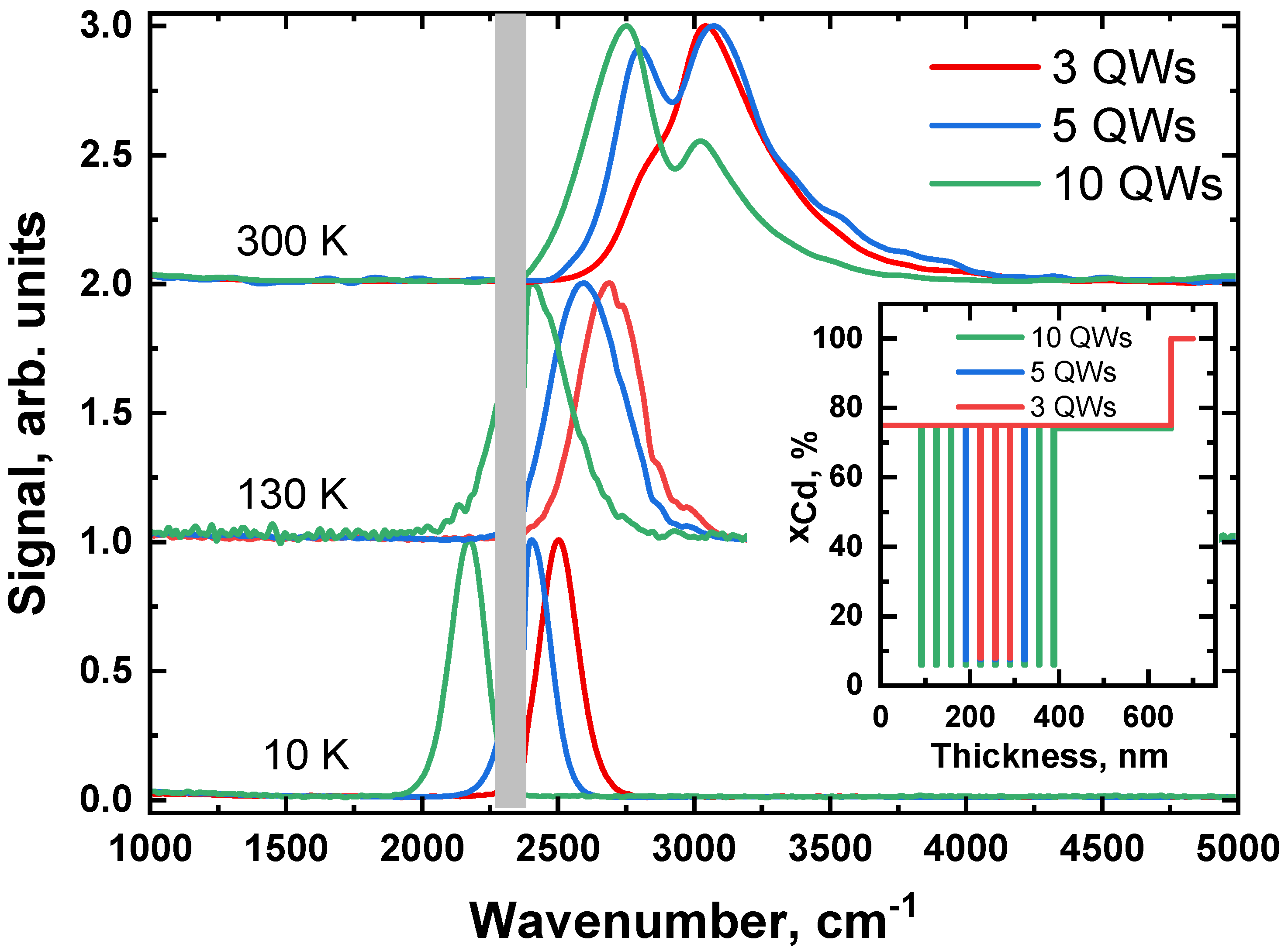
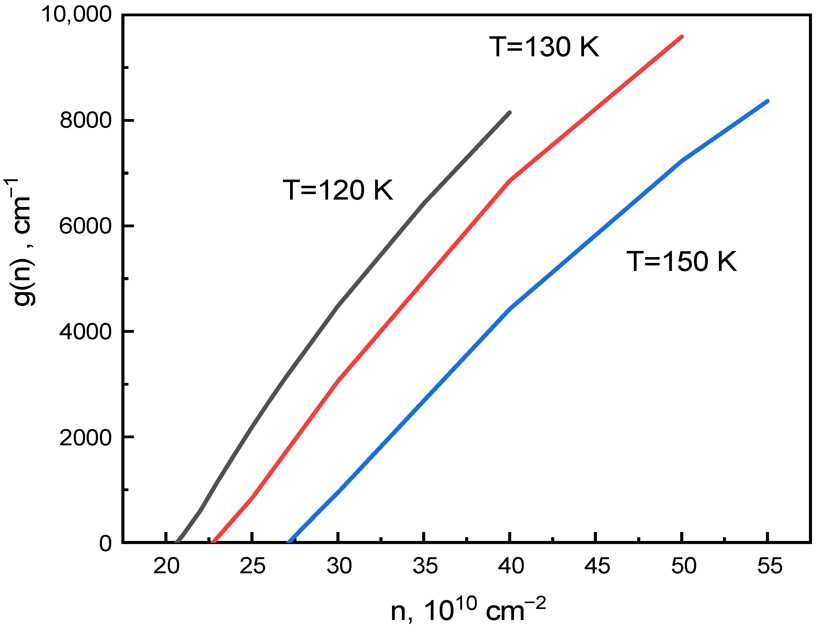
3. Results
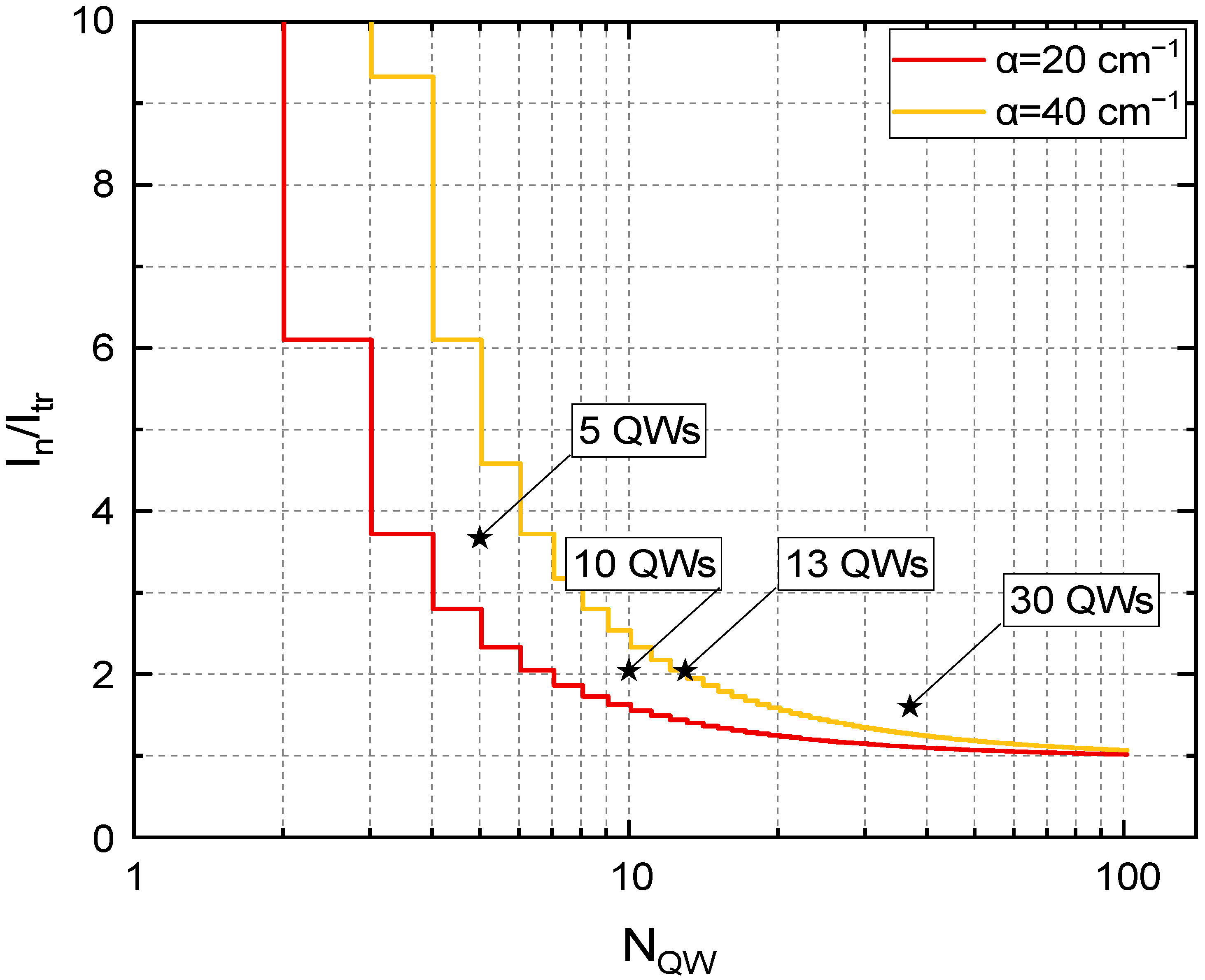
4. Discussion
Supplementary Materials
Author Contributions
Funding
Institutional Review Board Statement
Informed Consent Statement
Data Availability Statement
Conflicts of Interest
References
- Gordon, I.E.; Rothman, L.S.; Hill, C.; Kochanov, R.V.; Tan, Y.; Bernath, P.F.; Birk, M.; Boudon, V.; Campargue, A.; Chance, K.V.; et al. The HITRAN2016 Molecular Spectroscopic Database. J. Quant. Spectrosc. Radiat. Transf. 2017, 203, 3–69. [Google Scholar] [CrossRef]
- Vitiello, M.S.; Scalari, G.; Williams, B.; De Natale, P. Quantum Cascade Lasers: 20 Years of Challenges. Opt. Express 2015, 23, 5167. [Google Scholar] [CrossRef] [PubMed]
- Bandyopadhyay, N.; Bai, Y.; Tsao, S.; Nida, S.; Slivken, S.; Razeghi, M. Room Temperature Continuous Wave Operation of Λ~3–3.2 μm Quantum Cascade Lasers. Appl. Phys. Lett. 2012, 101, 18799–18806. [Google Scholar] [CrossRef]
- Bandyopadhyay, N.; Bai, Y.; Slivken, S.; Razeghi, M. High Power Operation of λ~5.2–11 Μm Strain Balanced Quantum Cascade Lasers Based on the Same Material Composition. Appl. Phys. Lett. 2014, 105, 071106. [Google Scholar] [CrossRef]
- Jung, D.; Bank, S.; Lee, M.L.; Wasserman, D. Next-Generation Mid-Infrared Sources. J. Opt. 2017, 19, 123001. [Google Scholar] [CrossRef] [Green Version]
- Belenky, G.; Shterengas, L.; Kipshidze, G.; Hosoda, T. Type-i Diode Lasers for Spectral Region above 3 Μm. IEEE J. Sel. Top. Quantum Electron. 2011, 17, 1426–1434. [Google Scholar] [CrossRef]
- Vizbaras, K.; Amann, M.C. Room-Temperature 3.73 Μm GaSb-Based Type-I Quantum-Well Lasers with Quinternary Barriers. Semicond. Sci. Technol. 2012, 27, 032001. [Google Scholar] [CrossRef]
- Veerabathran, G.K.; Sprengel, S.; Andrejew, A.; Amann, M.C. Room-Temperature Vertical-Cavity Surface-Emitting Lasers at 4 Μm with GaSb-Based Type-II Quantum Wells. Appl. Phys. Lett. 2017, 110, 071104. [Google Scholar] [CrossRef]
- Meyer, J.R.; Bewley, W.W.; Canedy, C.L.; Kim, C.S.; Kim, M.; Merritt, C.D.; Vurgaftman, I. The Interband Cascade Laser. Photonics 2020, 7, 75. [Google Scholar] [CrossRef]
- Yang, R.Q. Interband Cascade (IC) Lasers; Woodhead Publishing Limited: Cambridge, UK, 2013; ISBN 9780857091215. [Google Scholar]
- Preier, H. Recent Advances in Lead-Chalcogenide Diode Lasers. Appl. Phys. 1979, 20, 189–206. [Google Scholar] [CrossRef]
- Maremyanin, K.V.; Ikonnikov, A.V.; Bovkun, L.S.; Rumyantsev, V.V.; Chizhevskii, E.G.; Zasavitskii, I.I.; Gavrilenko, V.I. Terahertz Injection Lasers Based on a PbSnSe Solid Solution with an Emission Wavelength up to 50 Μm and Their Application in the Magnetospectroscopy of Semiconductors. Semiconductors 2018, 52, 1590–1594. [Google Scholar] [CrossRef]
- Meyer, J.R.; Canedy, C.L.; Kim, M.; Kim, C.S.; Merritt, C.D.; Bewley, W.W.; Vurgaftman, I. Comparison of Auger Coefficients in Type i and Type II Quantum Well Midwave Infrared Lasers. IEEE J. Quantum Electron. 2021, 57, 1–10. [Google Scholar] [CrossRef]
- Mami, F.Z.; Kadri, A.; Mokdad, N.; Zitouni, K. Nonparabolicity Effects on Carrier Lifetimes in Bulk Hg1-XCdxTe Alloys and Mid-Infrared 2D Hg1-XCdxTe/CdTe Single Quantum Well Lasers. Superlattices Microstruct. 2021, 150, 106780. [Google Scholar] [CrossRef]
- Kudryavtsev, K.E.; Rumyantsev, V.V.; Aleshkin, V.Y.; Dubinov, A.A.; Utochkin, V.V.; Fadeev, M.A.; Mikhailov, N.N.; Alymov, G.; Svintsov, D.; Gavrilenko, V.I.; et al. Temperature Limitations for Stimulated Emission in 3–4 μm Range Due to Threshold and Non-Threshold Auger Recombination in HgTe/CdHgTe Quantum Wells. Appl. Phys. Lett. 2020, 117, 083103. [Google Scholar] [CrossRef]
- Zegrya, G.G.; Polkovnikov, A.S. Mechanisms of Auger Recombination in Quantum Wells. J. Exp. Theor. Phys. 1998, 86, 815–832. [Google Scholar] [CrossRef]
- Vurgaftman, I.; Meyer, J. High-Temperature HgTe/CdTe Multiple-Quantum-Well Lasers. Opt. Express 1998, 2, 137. [Google Scholar] [CrossRef] [PubMed]
- Utochkin, V.V.; Kudryavtsev, K.E.; Dubinov, A.A.; Fadeev, M.A.; Rumyantsev, V.V.; Razova, A.A.; Andronov, E.V.; Aleshkin, V.Y.; Gavrilenko, V.I.; Mikhailov, N.N.; et al. Stimulated Emission up to 2.75 Μm from HgCdTe/CdHgTe QW Structure at Room Temperature. Nanomaterials 2022, 12, 2599. [Google Scholar] [CrossRef] [PubMed]
- Afonenko, A.A.; Ushakov, D.V.; Dubinov, A.A.; Aleshkin, V.Y.; Morozov, S.V.; Gavrilenko, V.I. Hot Phonon Effects and Auger Recombination on 3 μ m Room Temperature Lasing in HgTe-Based Multiple Quantum Well Diodes. J. Appl. Phys. 2022, 132, 073103. [Google Scholar] [CrossRef]
- Mikhailov, N.N.; Smirnov, R.N.; Dvoretsky, S.A.; Sidorov, Y.G.; Shvets, V.A.; Spesivtsev, E.V.; Rykhlitski, S.V. Growth of Hg1-XCdxTe Nanostructures by Molecular Beam Epitaxy with Ellipsometric Control. Int. J. Nanotechnol. 2006, 3, 120–130. [Google Scholar] [CrossRef]
- Dvoretsky, S.A.; Mikhailov, N.N.; Ikusov, D.G.; Kartashev, V.A.; Kolesnikov, A.V.; Sabinina, I.V.; Sidorov, Y.G.; Shvets, V.A. The Growth of CdTe Layer on GaAs Substrate by MBE; Nánai, L., Samantara, A., Fábián, L., Ratha, S., Eds.; IntechOpen: Rijeka, Croatia, 2019; pp. 1–12. ISBN 978-1-78985-860-0. [Google Scholar]
- Dvoretsky, S.; Mikhailov, N.; Sidorov, Y.; Shvets, V.; Danilov, S.; Wittman, B.; Ganichev, S. Growth of HgTe Quantum Wells for IR to THz Detectors. J. Electron. Mater. 2010, 39, 918–923. [Google Scholar] [CrossRef]
- Rumyantsev, V.V.; Razova, A.A.; Bovkun, L.S.; Tatarskiy, D.A.; Mikhailovskii, V.Y.; Zholudev, M.S.; Ikonnikov, A.V.; Uaman-Svetikova, T.; Maremyanin, K.V.; Utochkin, V.V.; et al. Optical Studies and Transmission Electron Microscopy of Hgcdte Quantum Well Heterostructures for Very Long Wavelength Lasers. Nanomaterials 2021, 11, 1855. [Google Scholar] [CrossRef] [PubMed]
- Aleshkin, V.Y.; Dubinov, A.A.; Rumyantsev, V.V.; Fadeev, M.A.; Domnina, O.L.; Mikhailov, N.N.; Dvoretsky, S.A.; Teppe, F.; Gavrilenko, V.I.; Morozov, S.V. Radiative Recombination in Narrow Gap HgTe/CdHgTe Quantum Well Heterostructures for Laser Applications. J. Phys. Condens. Matter. 2018, 30, 495301. [Google Scholar] [CrossRef] [PubMed]


| T, K | I3/I5 | I5/I10 | G, nm | ntr, cm−2 | α, cm−1 |
|---|---|---|---|---|---|
| 10 | 1.3 ± 0.7 | 0.7 ± 0.4 | -- | -- | -- |
| 30 | 1.5 ± 0.8 | 0.9 ± 0.6 | -- | -- | -- |
| 50 | 2.4 ± 1.1 | 1 ± 0.6 | -- | -- | -- |
| 70 | 2.3 ± 1 | 1 ± 0.5 | -- | -- | -- |
| 90 | 2.8 ± 1.2 | 1 ± 0.5 | -- | -- | -- |
| 110 | 3.4 ± 0.8 | 1.2 ± 0.45 | 0.49 | 2.3 * 1011 | 10 ± 16 |
| 130 | -- | 1.6 ± 0.5 | 0.36 | 2.3 * 1011 | 22.5 ± 18 |
| 150 | -- | 1.7 ± 0.4 | 0.32 | 2.9 * 1011 | 36.5 ± 9 |
Publisher’s Note: MDPI stays neutral with regard to jurisdictional claims in published maps and institutional affiliations. |
© 2022 by the authors. Licensee MDPI, Basel, Switzerland. This article is an open access article distributed under the terms and conditions of the Creative Commons Attribution (CC BY) license (https://creativecommons.org/licenses/by/4.0/).
Share and Cite
Fadeev, M.A.; Dubinov, A.A.; Razova, A.A.; Yantser, A.A.; Utochkin, V.V.; Rumyantsev, V.V.; Aleshkin, V.Y.; Gavrilenko, V.I.; Mikhailov, N.N.; Dvoretsky, S.A.; et al. Balancing the Number of Quantum Wells in HgCdTe/CdHgTe Heterostructures for Mid-Infrared Lasing. Nanomaterials 2022, 12, 4398. https://doi.org/10.3390/nano12244398
Fadeev MA, Dubinov AA, Razova AA, Yantser AA, Utochkin VV, Rumyantsev VV, Aleshkin VY, Gavrilenko VI, Mikhailov NN, Dvoretsky SA, et al. Balancing the Number of Quantum Wells in HgCdTe/CdHgTe Heterostructures for Mid-Infrared Lasing. Nanomaterials. 2022; 12(24):4398. https://doi.org/10.3390/nano12244398
Chicago/Turabian StyleFadeev, Mikhail A., Alexander A. Dubinov, Anna A. Razova, Arina A. Yantser, Vladimir V. Utochkin, Vladimir V. Rumyantsev, Vladimir Ya. Aleshkin, Vladimir I. Gavrilenko, Nikolai N. Mikhailov, Sergey A. Dvoretsky, and et al. 2022. "Balancing the Number of Quantum Wells in HgCdTe/CdHgTe Heterostructures for Mid-Infrared Lasing" Nanomaterials 12, no. 24: 4398. https://doi.org/10.3390/nano12244398