Article

Direct Detection of Inhomogeneity in CVD-Grown 2D TMD Materials via K-Means Clustering Raman Analysis

1
School of Physics & Optoelectronic Engineering, Nanjing University of Information Science & Technology, Nanjing 210044, China
2
Jiangsu Key Laboratory for Optoelectronic Detection of Atmosphere and Ocean, Nanjing University of Information Science & Technology, Nanjing 210044, China
3
Jiangsu International Joint Laboratory on Meterological Photonics and Optoelectronic Detection, Nanjing University of Information Science & Technology, Nanjing 210044, China
*
Author to whom correspondence should be addressed.
Nanomaterials 2022, 12(3), 414; https://doi.org/10.3390/nano12030414
Submission received: 11 November 2021 / Revised: 24 December 2021 / Accepted: 6 January 2022 / Published: 27 January 2022
(This article belongs to the Special Issue Optical Properties and Applications of 2D Nanostructures)

Abstract

:
It is known that complex growth environments often induce inhomogeneity in two-dimensional (2D) materials and significantly restrict their applications. In this paper, we proposed an efficient method to analyze the inhomogeneity of 2D materials by combination of Raman spectroscopy and unsupervised k-means clustering analysis. Taking advantage of k-means analysis, it can provide not only the characteristic Raman spectrum for each cluster but also the cluster spatial maps. It has been demonstrated that inhomogeneities and their spatial distributions are simultaneously revealed in all CVD-grown MoS2, WS2 and WSe2 samples. Uniform p-type doping and varied tensile strain were found in polycrystalline monolayer MoS2 from the grain boundary and edges to the grain center (single crystal). The bilayer MoS2 with AA and AB stacking are shown to have relatively uniform p-doping but a gradual increase of compressive strain from center to the periphery. Irregular distribution of 2 L A ( M ) / E 2 g 1 mode in WS2 and E 2 g 1 mode in WSe2 is revealed due to defect and strain, respectively. All the inhomogeneity could be directly characterized in color-coded Raman imaging with correlated characteristic spectra. Moreover, the influence of strain and doping in the MoS2 can be well decoupled and be spatially verified by correlating with the clustered maps. Our k-means clustering Raman analysis can dramatically simplify the inhomogeneity analysis for large Raman data in 2D materials, paving the way towards direct evaluation for high quality 2D materials.

1. Introduction

Two-dimensional (2D) transition metal dichalcogenides (TMD), MX2 (M = Mo, W and X = S, Se, etc.), have attracted considerable attention due to their unique physical and chemical properties, exhibiting promising applications on optoelectronics [1,2,3], valley-electronics [4] and chemical sensors [5,6]. Both fundamental research and potential applications are highly dependent on the quality of TMD materials [7,8,9,10]. Conventionally, there are two kinds of methods to prepare 2D materials: top-down and bottom-up approaches. The typical top-down method, mechanical cleavage with scotch tape [7,8], could give high-quality mono- and few-layer TMD materials with limited size preventing their actual applications. On the other hands, bottom-up synthesis methods (such as intercalation assisted exfoliation [11], physical vapor deposition [12], hydrothermal synthesis [13], and chemical vapor deposition (CVD)) can offer a lateral size of TMD films up to hundreds of micrometers. In particular, CVD has been well-developed to produce large area crystals with controllable thickness and stacking sequences [9,10,14]. As a matter of fact, it is still a challenge to obtain highly uniform TMD materials with high performance on carrier mobility and conductivity with the CVD method. Due to the complicated growth processes in CVD and the interfacial interaction with substrate, mono- and few-layer TMD materials often host various inhomogeneities such as defects, strain and doping [15,16,17,18,19,20], which affects their mobility and electronic properties [21,22,23,24,25]. These common issues call for a direct characterization of local inhomogeneity in CVD-grown TMD materials.
Raman spectroscopy has been demonstrated as an effective and non-destructive method to characterize layered materials, such as graphene and TMD materials. The characteristic Raman bands of TMD materials represent the change of layer thickness [8,26], charge doping [27,28,29], defects [30,31], and strain [32,33,34]. Conley et al. observed the red-shifting of E 2 g 1 mode from mono- to bi-layer MoS2 when applying uniaxial tensile strain [32]. Parkin et al. reported that the Raman characteristic mode shift can be used as a means to evaluate the sulfur vacancies in MoS2 [27]. Moreover, Chae W.H. and coworkers used the Raman spectral correlations to analyze the strain and doping in single-layer MoS2 grown by CVD method [35].
However, these studies were based on the Raman measurements at multiple points selected in a random way which is not applicable for samples with uniform optical contrast. The traditional Raman imaging is very useful for TMD material characterization [8,36]. However, it isn’t so efficient to do advanced spectral fitting, especially when dealing with thousands of Raman data of large size TMD. Another difficulty emerges when we try to decouple the strain and doping effects and further correlate them with sample areas. Therefore, it is essential to present a simple and efficient method to evaluate the material quality and probe the detailed inhomogeneity information.
As one of the most prevalent multivariate and unsupervised methods, k-means clustering is well-developed and has been applied to bio-Raman analysis [37,38]. The clustering is established from the spectral similarities reflecting all Raman spectral bands information, such as peak intensity, peak position, and peak width. In this work, we proposed an unsupervised k-means clustering Raman analysis [39] to directly identify the inhomogeneity in MoS2, WS2 and WSe2 samples grown by the CVD method. The whole spectral features of all Raman bands were selected for automatic clustering to keep the integrity. Based on the Raman spectral similarity, the clustered maps and several representative Raman spectra for each cluster could be obtained. The Raman spectral parameters in all clustered results are then correlated to evaluate the influences of strain and doping quantitatively in each clustered area. Varied strain-induced inhomogeneities and uniform p-type doping were observed in monolayer MoS2 with polycrystalline structure. With the help of k-means clustering, the bilayer MoS2 with AA and AB stacking were verified with four typical areas from center to periphery with a gradual increase of compressive strain and uniform p-doping. We also extended such analysis to probe the inhomogeneity in monolayer WS2 and WSe2. Non-uniform distribution of 2 L A ( M ) / E 2 g 1 mode in WS2 and E 2 g 1 mode in WSe2 is observed which is caused by strain. All the inhomogeneity mentioned above were directly visualized in color-coded Raman imaging with the correlated characteristic spectra. Combination of Raman spectroscopy with k-means clustering was proven to be efficient to distinguish the inhomogeneities distributions in the 2D materials caused by strain and doping. These results have demonstrated to be important for quality check in CVD-grown TMD and pave the way towards the high-performance TMD devices.

2. Experimental Section

MoS2, WS2 and WSe2 were grown by CVD on Si substrates with a 300 nm thick SiO2 [40]. Raman spectra and imaging were carried out using a confocal Raman microscope (WITec Alpha 300R, Ulm, Germany) equipped with the excitation source of 532 nm and a UHTS 300 spectrometer with 300 mm focal length. The laser beam was focused on the sample via 100 × 0.9 objective lens with the lateral spatial resolution better than 350 nm. The signal was collected through the same lens, dispersed with a 2400 grooves/mm grating for Raman spectra and was eventually detected by a FI-CCD camera with 1600 × 200 pixels (Andor) cooled to −60 °C. It could provide good spectral resolution 1.0 cm−1 and high repeatability better than 0.02 cm−1, which guarantees sufficient accuracy for the inhomogeneity analysis. The laser power was set to be 0.5 mW avoiding any damage on sample. All the Raman imaging data was classified by clustering and then statistically correlated via WITec Project Five software.

3. The K-Means Clustering and Inhomogeneity Visualization for Confocal Raman Analysis

The algorithm of k-means clustering aims at dividing the 2D, two-way data into the given K classes ( C 1 ,   C 2 ,   .   .   .   , C k ), where C k is the set of n k objects in cluster k . There are N = I × J total spectra and each one has a measurement of the P variable-spectral points in pixels in which I and J are the number of pixels or the number of the measurements along the I and J-coordinates. The centroid of the cluster C k is a point in the P-dimensional space, which is calculated by averaging the values of each variable on the objects in the cluster. For example, the centroid value of the j th variable in the cluster C k is
x ¯ j ( k ) = 1 n k i C k x i j ,
And the complete centroid vector of cluster C is
x ¯ ( k ) = ( x ¯ 1 ( k ) , x ¯ 2 ( k ) , , x ¯ p ( k ) )
The typical k-means clustering algorithm operates through the following iterative process:
(1)
The P-dimensional vector ( s 1 ( k ) ,     , s p ( k ) ) defines K initial seeds, for 1 < k   < K , and the squared Euclidean distance, d2( i , k ) (between the i th object and the k th seed vector) is obtained: d 2 ( i ,   k ) = j = 1 p ( x i j s j ( k ) ) 2 .
(2)
Assign spectra to the smallest cluster. After initial Raman spectra allocation, the following operation is to obtain the cluster centroid for each cluster. All spectra are compared to each centroid (using d2( i , k )) and moved to the cluster whose centroid is the closest.
(3)
Use the updated cluster membership to calculate the new centroid (by calculating the centroids after all spectra have been assigned).
(4)
Steps 2 and 3 are repeated until each cluster no longer changes.
(5)
As illustrated in Figure 1a,b, 2D Raman spectra was collected via point scanning on TMD materials. In the 3D data set, there are N = I × J total spectra with p = 1600 spectral points in wavenumber unit. As shown in Figure 1c, in order to ensure the clustering accuracy, the Raman spectral range was particularly selected and the spectral points were reduced to P (range of characteristic peaks of TMD materials). For example, all Raman spectra could be finally divided into three categories (cluster I, II, III) through k-means clustering as shown in Figure 1d. The cluster spatial maps and the correlated mean spectra are shown in Figure 1e. Such classification is based on the similarity of whole spectral features (peak intensity, peak position and width).

4. Results and Discussion

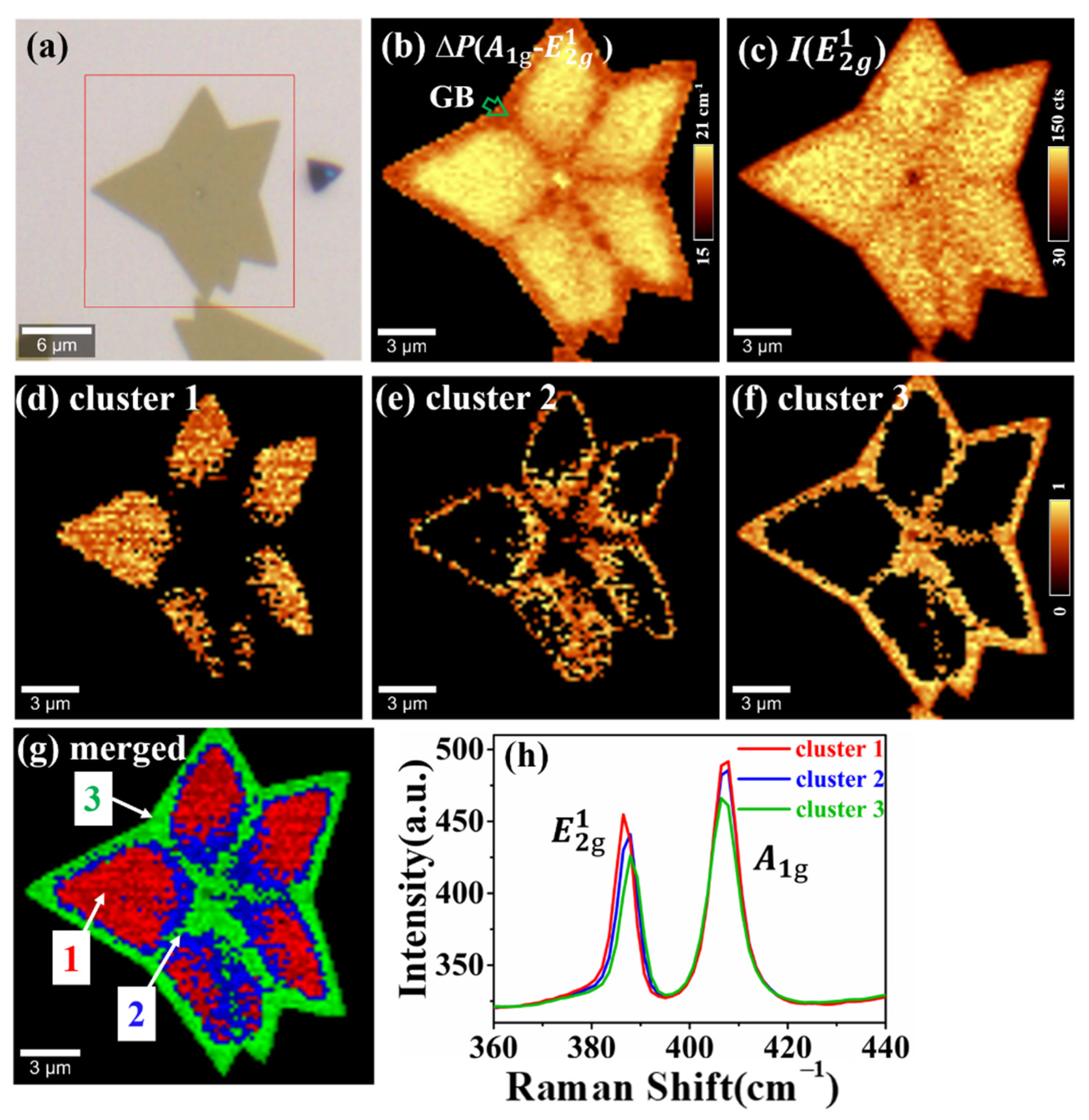
4.1. K-Means Raman Analysis of Monolayer MoS2

We probe inhomogeneity in monolayer CVD-grown MoS2 through the combination of Raman spectroscopy and k-means clustering, as shown in Figure 2. An optical image of the MoS2 sample is displayed in Figure 2a. Confocal Raman imaging was conducted on an 18 × 18 μm2 area with 200 nm step size and 8100 spectra were gained in total. It can be inferred that the overall frequency difference between A 1 g (out-of-plane) and E 2 g 1 (in-plane) modes is about 15~21 cm−1 as shown in Figure 2b which is consistent with the previous report on monolayer MoS2 [41]. On the other hand, we noticed that the A 1 g mode shows uniform distribution around 404 cm−1 only with slightly lower frequency along grain boundaries (GB) and sample edges as displayed in Figure S1e in supplemental material. On the contrary, the E 2 g 1 mode shows prominent red shift from GB and sample edge to grain center, as inferred from Figure S1a in supplemental material, indicating irregular tensile strain distribution from GB to grain center. The E 2 g 1 and A 1 g modes are often correlated with uniaxial strains [32,33] and charge doping [27,28], respectively. Hence, we can conclude that dominant tensile strain and slight doping condition coexist in this monolayer MoS2. The tensile strains could result from the different thermal expansion coefficients of the substrate during CVD growth [16]. However, the influence of strain and doping effects on peak intensities and peak width remains unknown. Moreover, such Raman measurements and analysis always require expertise and much effort to extract useful information, especially when dealing with tremendous Raman data in large size TMD. Here, we applied an efficient method to obtain a more comprehensive understanding of all these complicate images and check material quality directly.
We re-evaluated the Raman spectra using k-means clustering analysis, which could give a rapid classification between data points via squared Euclidean distance. The two characteristic Raman modes of MoS2,   A 1 g and E 2 g 1 , were both selected and the Raman data were automatically analyzed. It turned out that the 8100 spectra were eventually classified into three clusters. The mean Raman spectra and the corresponding cluster spatial maps are shown in Figure 2d–f,h, respectively. The E 2 g 1 modes of cluster 1–3 were located at 383.9, 384.6, and 385.3 cm−1, respectively, while the A 1 g mode was almost at 404 cm−1 through Lorentz function fitting, as shown in Table S1 in Supplementary Materials. These cluster spectra could easily reveal the gradient trend of strain distributions in the whole sample, cluster 1 > cluster 2 > cluster 3, which is impossible to distinguish from E12g mode in the traditional Raman analysis in Figure S1a. Obviously, the k-means clustering could classify Raman data and also dramatically reduce the spectral data analysis from thousands of spectra to a few ones. Meanwhile, by merging the cluster maps, the inhomogeneity could be easily recognized in a color-coded image, as shown in Figure 2g, providing direct visualization for the evaluation of sample quality.
The correlation analysis of Raman spectral features has been extensively utilized to decouple the strain and doping effect of graphene and TMD materials [42]. Michail et al. plotted a correlation graph between Pos( E 2 g 1 ) and Pos( A 1 g ) to distinguish the strain and doping contributions in monolayer MoS2 prepared by mechanical exfoliation [43]. They manually allocated the sample area by optical contrast or conspicuous defect positions and then artificially subdivided the sample into several areas. Apparently, such manual selections are in-debate due to low precision. Moreover, it does not work for uniform optical images in which the sample inhomogeneity cannot be directly discerned, as shown in Figure 2a. Fortunately, the k-means method plays an important role in analyzing Raman spectral features of TMD materials with homogeneous optical contrast. The clustered correlation graphs were plotted as a function of peak position (Pos( E 2 g 1 ), Pos( A 1 g )) and peak width ( E 2 g 1 ) to further evaluate the strain and doping effects. For better comparison, the original and clustered Raman data were firstly displayed in 3D, as shown in Figure 3a,b, respectively. Obviously, the clustered distribution map between E 2 g 1 and A 1 g peak positions clearly revealed more information about the inhomogeneity of MoS2 induced by strain and doping effects. By adopting the same method with Michail’s work, the distribution of strain and doping was further calculated by comparing their linear and independent influences on peak positions, as shown in Figure 3c. The ε   ~   n   ( ε and n represent functions of strain and charge carrier concentration, respectively) relationships are calculated by choosing the Grüneisen parameters (0.86 for E 2 g 1 and 0.15 for A 1 g modes) and the carrier concentration (−0.33 × 10⁻¹³ cm−2 for E 2 g 1 and −2.22 × 10⁻¹³ cm−2 for A 1 g modes) [43,44,45]. The frequencies of E 2 g 1 (384.7 cm−1) and A 1 g (402.7 cm−1) with 532 nm laser was selected as the unperturbed phonon frequencies in our calculations. The strain range in cluster 1–3 was 0.1~0.2%, 0~0.1% and 0.1~−0.1%, respectively. The overall p-doping concentration was about 0.5~1.0 × 10⁻¹³ cm−2, which may result from the absence of sulfur atoms and sulfur vacancies occupied by oxygen atoms during the CVD growth process [31].

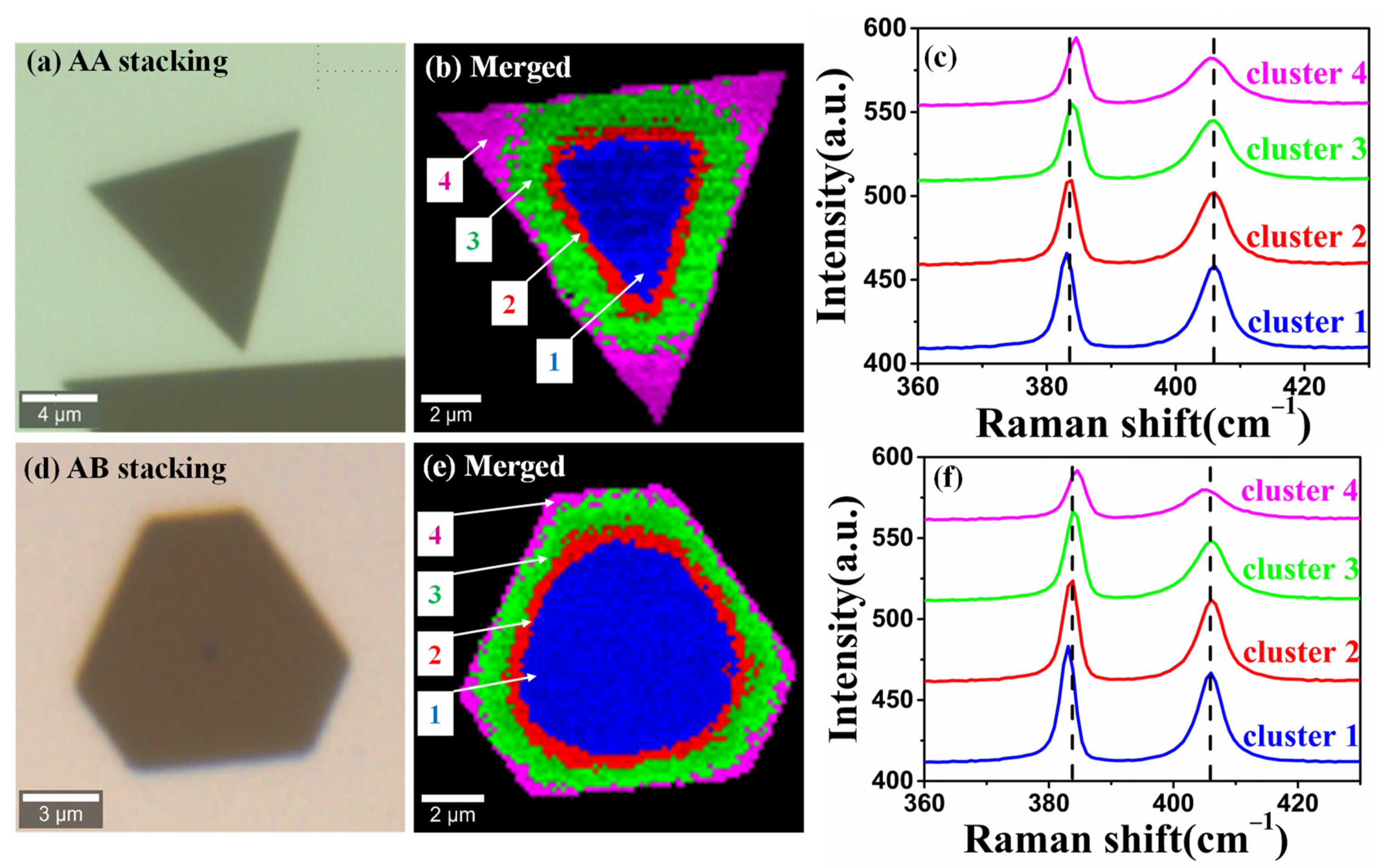
4.2. K-Means Raman Analysis of Bilayer MoS2 with Different Stacking

It is well-known that the stacking order of TMD materials plays an important role in their physical and chemical properties [46,47,48]. Therefore, we further apply k-means cluster analysis to visualize the inhomogeneity of the CVD-grown bilayer MoS2 with different stacking. Confocal Raman imaging was conducted on a 12.5 × 12.5 μm2 area with 150 nm step size and 7225 spectra were gathered. Optical images of bilayer MoS2 with different stacking were displayed in Figure 4a,d, which were identified based on the relative intensity ratios of the breathing and shear modes in low wavenumber polarized Raman (as shown in Figure S2) [49]. The behavior of strain and doping inhomogeneity in the bilayer MoS2 with two different stacking are similar. Here, we only discussed the situation in triangular bilayers of MoS2 with AA stacking.
The k-means cluster analysis and corresponding Raman spectra are shown in Figure 4b,c,e,f. The samples were grouped into four regions (cluster 1, cluster 2, cluster 3, and cluster 4), as displayed in Figure 4b,e. Here we used the frequencies of E 2 g 1 (382.5 cm−1) and A 1 g (404.9 cm−1) with 532 nm laser as the unperturbed phonon frequencies of bilayer MoS2. For AA stacking, the mean frequencies of the E 2 g 1 mode of cluster 1–4 are 383.1, 383.6, 384.1 and 384.5 cm−1 as illustrated in Figure 4c.
We noted that the peak position of the E 2 g 1 mode gradually shifted towards higher wavenumber from cluster 1 to cluster 4, indicating an increased compressive strain from center to periphery. The strain state of these two bilayer MoS2 samples is consistent with the results of Luo et al. [17]. This might be induced by different thermal expansion coefficients between the substrate and MoS2 during the CVD growth. There is no shift of A 1 g mode from cluster 1 to 4. Interestingly, we found the full width at half maximum (FWHM) of A 1 g mode becomes broader, indicating the increase of doping concentrations from cluster 1 to cluster 4. P-type doping MoS2 with AA stacking is evidenced by the overall blue shift of A 1 g mode compared with the unperturbed phonon frequencies in Figures S3a and S4a in supplemental materials. All in all, the clustered correlation analysis offers a solution to the cluster spatial map and further decouple and quantify the inhomogeneity of strain and doping effects.

4.3. K-Means Raman Analysis of Monolayer WS2 and WSe2

We further apply the k-means clustering Raman analysis to visualize the inhomogeneity in monolayer WS2 and WSe2. The optical images of triangular monolayer WS2 and WSe2 on Si/SiO2 substrate grown by the CVD method show a very homogeneous contrast, as illustrated in Figure 5a,d. Confocal Raman imaging of WS2 and WSe2 were conducted on a 20 × 20 μm2 area with 200 nm step size and 9775 and 9500 spectra were obtained, respectively. When excited with 532 nm laser, their resonance Raman spectra became much more complex, with several second-order Raman modes and a first-order prominent one as 2 L A ( M ) / E 2 g 1 mode in WS2 and E 2 g 1 in WSe2, as shown in Figure 5g,h. Their peak positions coincided with the previous Raman measurements, confirming their monolayer TMD structure [50,51]. The traditional Raman images of the prominent 2 L A ( M ) / E 2 g 1 and E 2 g 1 peak intensity for WS2 and WSe2 plotted in Figure 5b,e cannot manifest any inhomogeneities. With the help of k-means clustering, the local inhomogeneity can be clearly identified via the mean Raman spectra and then visualized through the color-coded Raman image. In the case of WS2, the triangle sample could be classified into two groups, cluster 1 and cluster 2, as displayed in Figure 5c. Comparing with cluster 1, it can be easily seen that the cluster 2 had higher intensity of the 2 L A ( M ) to E 2 g 1 as displayed in Figure 5g. It might have resulted from the local nanocrystallities formation with different sizes during CVD growth, as in the observation on single-layer WS2 treated by ion implantation by Tan, P.H. and his co-workers [52]. It is difficult to obtain more specific information of strain and doping, due to the complexity of the resonant excitation of WS2 under 532 nm. While in the monolayer WSe2 sample, the clustered results in Figure 5f,h exhibit three different areas with minor spectral shifting of E 2 g 1 peak position, indicating the different level of strain during the CVD process (cluster 1 > cluster 2 > cluster 3). Another peak appeared on the shoulder of the E 2 g 1 peak due to the effect of strain. The E 2 g 1 peak split into two peaks, E 2 g + and E 2 g , representing the in-plane atomic vibrations in orthogonal and parallel ways, respectively. The spectral shifting of the E 2 g 1 peak was similar to the result of Tang N. Y. et al. [53], which can be further confirmed as tensile strain. Remarkably, the k-means clustering Raman analysis could benefit for directly visualizing the existence of the inhomogeneity in TMD layered materials in a high accuracy and efficient way, providing important quality-control for TMD materials by the CVD method.

5. Conclusions

In this paper, we have successfully demonstrated that the combination of k-means clustering and Raman analysis was able to rapidly reveal the inhomogeneity distribution in the CVD-grown MoS2, WS2 and WSe2 layered materials. The k-means clustering method can provide the color-coded clustered Raman maps and corresponding mean Raman spectra. It could be beneficial to further identify the origin of various inhomogeneities. Introducing k-means analysis with correlations enables us to decouple and quantitatively evaluate the strain and doping contributions quantitatively in clusters. For the polycrystalline monolayer MoS2, there were obvious tensile strain and uniform p-type doping from the GB and edges to each grain center (single crystal). The bilayer MoS2 with AA and AB stacking was found with relatively uniform p-type doping and a gradual increase in compressive strain from center to periphery. In the case of monolayer WS2 and WSe2, we observed a non-uniform distribution of inhomogeneity of the 2 L A ( M ) / E 2 g 1 mode and the E 2 g 1 mode due to defect and strain, respectively. Our Raman analysis together with k-means clustering suggest that it is possible to directly detect the inhomogeneities and quantitatively evaluate the contributions of strain and doping in TMD materials. We expect that such automatic and unsupervised Raman analysis could be utilized to characterize the inhomogeneity and optimize TMD materials during the CVD process in order to obtain high performance devices.

Supplementary Materials

The following are available online at https://www.mdpi.com/article/10.3390/nano12030414/s1, Figure S1: (a–c,e–g) are Raman images of monolayer polycrystalline MoS2 plotted as a function of the peak position (P), width (W), and intensity (I) of E 2 g 1 and A 1 g modes. The difference between E 2 g 1 and A 1 g modes in peak position and relative peak intensities are calculated and plotted in (d,h). Table S1: Raman parameters of the cluster 1–3 in monolayer polycrystalline MoS2 sample fitted with Lorentz function. Figure S2: Stacking identification of AA and AB bilayer MoS2 by polarized Raman spectroscopy. (a,b) Optical image of CVD-grown bilayer MoS2 and (c,d) the correlated Stoke and anti-Stoke low wavenumber Raman spectra measured under parallel (//) and cross (⊥) polarization configurations, respectively. The AA and AB stacking orders could be extracted from the relative intensities between the shearing mode (SM) and breathing mode (BM) at 22.5 and 40.5 cm−1 in excellent agreement with X. Yan et al.’s work. Figure S3: Correlative analysis of Raman spectral features to quantitatively evaluate the contribution of strain and doping effects on bilayer MoS2 with AA-stacking. (a) The 2D correlative analysis of Pos( E 2 g 1 ) and Pos( A 1 g ) in cluster 1–4. (b) Correlation plot of FWHM( E 2 g 1 ) vs. Pos( E 2 g 1 ). (c) Correlation plot of FWHM( A 1 g ) vs. Pos( A 1 g ). (d) Correlation plot of AMP( A 1 g ) vs. AMP( E 2 g 1 ). Figure S4: Correlative analysis of Raman spectral features to quantitatively evaluate the contribution of strain and doping effects on monolayer MoS2 with AB stacking. The 2D correlative analysis of (a) Correlation plots of Pos( E 2 g 1 ) and Pos( A 1 g in cluster 1–4. (b–d) Correlation plots of FWHM( E 2 g 1 ) vs. Pos( E 2 g 1 ), FWHM( A 1 g ) vs. Pos( A 1 g ) and AMP( A 1 g ) vs. AMP( E 2 g 1 ), respectively.

Author Contributions

H.X. performed the Raman spectroscopy measurements. J.Z. supervised the project and analyzed the data with H.X., C.Y. and Y.C. revised the manuscript. All authors have read and agreed to the published version of the manuscript.

Funding

This research was funded by the National Natural Science Foundation of China (Grant No. 11604157).

Conflicts of Interest

The authors declare no conflict of interest.

References

  1. Liu, Y.; Weiss, N.O.; Duan, X.D.; Cheng, H.C.; Huang, Y.; Duan, X.F. Van der Waals heterostructures and devices. Nat. Rev. Mater. 2016, 1, 16042. [Google Scholar] [CrossRef]
  2. Novoselov, K.S.; Mishchenko, A.; Carvalho, A.; Neto, A.H.C. 2D materials and van der Waals heterostructures. Science 2016, 353, 6298. [Google Scholar] [CrossRef] [Green Version]
  3. Li, J.K.; Chen, Z.Q.; Yang, H.; Yi, Z.; Chen, X.F.; Yao, W.T.; Duan, T.; Wu, P.H.; Li, G.F.; Yi, Y.G. Tunable Broadband Solar Energy Absorber Based on Monolayer Transition Metal Dichalcogenides Materials Using Au Nanocubes. Nanomaterials 2020, 10, 257. [Google Scholar] [CrossRef] [Green Version]
  4. Zeng, H.L.; Cui, X.D. An optical spectroscopic study on two-dimensional group-VI transition metal dichalcogenides. Chem. Soc. Rev. 2015, 44, 2629–2642. [Google Scholar] [CrossRef]
  5. Zhang, Y.; Zheng, B.; Zhu, C.F.; Zhang, X.; Tan, C.L.; Li, H.; Chen, B.; Yang, J.; Chen, J.Z.; Huang, Y.; et al. Single-Layer Transition Metal Dichalcogenide NanosheetBased Nanosensors for Rapid, Sensitive, and Multiplexed Detection of DNA. Adv. Mater. 2015, 27, 935–939. [Google Scholar] [CrossRef]
  6. Sinha, A.; Dhanjai; Tan, B.; Huang, Y.J.; Zhao, H.M.; Dang, X.M.; Chen, J.P.; Jain, R. MoS2 nanostructures for electrochemical sensing of multidisciplinary targets: A review. TrAC-Trends Anal. Chem. 2018, 102, 75–90. [Google Scholar] [CrossRef]
  7. Splendiani, A.; Sun, L.; Zhang, Y.; Li, T.; Kim, J.; Chim, C.-Y.; Galli, G.; Wang, F. Emerging Photoluminescence in Monolayer MoS2. Nano Lett. 2010, 10, 1271–1275. [Google Scholar] [CrossRef]
  8. Li, H.; Zhang, Q.; Yap, C.C.R.; Tay, B.K.; Edwin, T.H.T.; Olivier, A.; Baillargeat, D. From Bulk to Monolayer MoS2: Evolution of Raman Scattering. Adv. Funct. Mater. 2012, 22, 1385–1390. [Google Scholar] [CrossRef]
  9. Li, T.; Guo, W.; Ma, L.; Li, W.; Yu, Z.; Han, Z.; Gao, S.; Liu, L.; Fan, D.; Wang, Z.; et al. Epitaxial growth of wafer-scale molybdenum disulfide semiconductor single crystals on sapphire. Nat. Nanotechnol. 2021, 16, 1201–1207. [Google Scholar] [CrossRef]
  10. Hong, S.; Zagni, N.; Choo, S.; Liu, N.; Baek, S.; Bala, A.; Yoo, H.; Kang, B.H.; Kim, H.J.; Yun, H.J.; et al. Highly sensitive active pixel image sensor array driven by large-area bilayer MoS2 transistor circuitry. Nat. Commun. 2021, 12, 3559. [Google Scholar] [CrossRef]
  11. Matte, H.; Gomathi, A.; Manna, A.K.; Late, D.J.; Datta, R.; Pati, S.K.; Rao, C.N.R. MoS2 and WS2 Analogues of Graphene. Angew. Chem. Int. Ed. 2010, 49, 4059–4062. [Google Scholar] [CrossRef]
  12. Lauritsen, J.V.; Kibsgaard, J.; Helveg, S.; Topsoe, H.; Clausen, B.S.; Laegsgaard, E.; Besenbacher, F. Size-dependent structure of MoS2 nanocrystals. Nat. Nanotechnol. 2007, 2, 53–58. [Google Scholar] [CrossRef]
  13. Duraisamy, S.; Ganguly, A.; Sharma, P.K.; Benson, J.; Davis, J.; Papakonstantinou, P. One-Step Hydrothermal Synthesis of Phase-Engineered MoS2/MoO3 Electrocatalysts for Hydrogen Evolution Reaction. ACS Appl. Nano Mater. 2021, 4, 2642–2656. [Google Scholar] [CrossRef]
  14. Shi, Y.M.; Li, H.N.; Li, L.J. Recent advances in controlled synthesis of two-dimensional transition metal dichalcogenides via vapour deposition techniques. Chem. Soc. Rev. 2015, 44, 2744–2756. [Google Scholar] [CrossRef]
  15. Kolesnichenko, P.V.; Zhang, Q.H.; Yun, T.H.; Zheng, C.X.; Fuhrer, M.S.; Davis, J.A. Disentangling the effects of doping, strain and disorder in monolayer WS2 by optical spectroscopy. 2D Mater. 2020, 7, 025008. [Google Scholar] [CrossRef] [Green Version]
  16. Kataria, S.; Wagner, S.; Cusati, T.; Fortunelli, A.; Iannaccone, G.; Pandey, H.; Fiori, G.; Lemme, M.C. Growth-Induced Strain in Chemical Vapor Deposited Monolayer MoS2: Experimental and Theoretical Investigation. Adv. Mater. Interfaces 2017, 4, 1700031. [Google Scholar] [CrossRef] [Green Version]
  17. Luo, S.W.; Cullen, C.P.; Guo, G.C.; Zhong, J.X.; Duesberg, G.S. Investigation of growth-induced strain in monolayer MoS2 grown by chemical vapor deposition. Appl. Surf. Sci. 2020, 508, 145126. [Google Scholar] [CrossRef] [Green Version]
  18. Hu, C.; Yuan, C.L.; Hong, A.J.; Guo, M.M.; Yu, T.; Luo, X.F. Work function variation of monolayer MoS2 by nitrogen-doping. Appl. Phys. Lett. 2018, 113, 041602. [Google Scholar] [CrossRef]
  19. Wang, W.D.; Yang, C.G.; Bai, L.W.; Li, M.L.; Li, W.B. First-Principles Study on the Structural and Electronic Properties of Monolayer MoS2 with S-Vacancy under Uniaxial Tensile Strain. Nanomaterials 2018, 8, 74. [Google Scholar] [CrossRef] [Green Version]
  20. Wei, H.L.; Gui, Y.G.; Kang, J.; Wang, W.B.; Tang, C. A DFT Study on the Adsorption of H2S and SO2 on Ni Doped MoS2 Monolayer. Nanomaterials 2018, 8, 646. [Google Scholar] [CrossRef] [Green Version]
  21. Zhang, C.D.; Johnson, A.; Hsu, C.L.; Li, L.J.; Shih, C.K. Direct Imaging of Band Profile in Single Layer MoS2 on Graphite: Quasiparticle Energy Gap, Metallic Edge States, and Edge Band Bending. Nano Lett. 2014, 14, 2443–2447. [Google Scholar] [CrossRef] [Green Version]
  22. Yuan, N.F.Q.; Mak, K.F.; Law, K.T. Possible Topological Superconducting Phases of MoS2. Phys. Rev. Lett. 2014, 113, 097001. [Google Scholar] [CrossRef] [Green Version]
  23. Cai, Y.Q.; Zhang, G.; Zhang, Y.W. Polarity-Reversed Robust Carrier Mobility in Monolayer MoS2 Nanoribbons. J. Am. Chem. Soc. 2014, 136, 6269–6275. [Google Scholar] [CrossRef] [Green Version]
  24. Zheng, J.Y.; Yan, X.X.; Lu, Z.X.; Qiu, H.L.; Xu, G.C.; Xu, Z.; Peng, W.; Pan, X.Q.; Liu, K.H.; Jiao, L.Y. High-Mobility Multilayered MoS2 Flakes with Low Contact Resistance Grown by Chemical Vapor Deposition. Adv. Mater. 2017, 29, 1604540. [Google Scholar] [CrossRef]
  25. Vojvodic, A.; Hinnemann, B.; Norskov, J.K. Magnetic edge states in MoS2 characterized using density-functional theory. Phys. Rev. B 2009, 80, 125416. [Google Scholar] [CrossRef] [Green Version]
  26. O’Brien, M.; McEvoy, N.; Hanlon, D.; Hallam, T.; Coleman, J.N.; Duesberg, G.S. Mapping of Low-Frequency Raman Modes in CVD-Grown Transition Metal Dichalcogenides: Layer Number, Stacking Orientation and Resonant Effects. Sci. Rep. 2016, 6, 19476. [Google Scholar] [CrossRef]
  27. Parkin, W.M.; Balan, A.; Liang, L.; Das, P.M.; Lamparski, M.; Naylor, C.H.; Rodríguez-Manzo, J.A.; Johnson, A.T.C.; Meunier, V.; Drndić, M. Raman Shifts in Electron-Irradiated Monolayer MoS2. ACS Nano 2016, 10, 4134–4142. [Google Scholar] [CrossRef] [Green Version]
  28. Lin, J.D.; Han, C.; Wang, F.; Wang, R.; Xiang, D.; Qin, S.; Zhang, X.-A.; Wang, L.; Zhang, H.; Wee, A.T.S.; et al. Electron-Doping-Enhanced Trion Formation in Monolayer Molybdenum Disulfide Functionalized with Cesium Carbonate. ACS Nano 2014, 8, 5323–5329. [Google Scholar] [CrossRef]
  29. Lee, J.S.; Park, C.S.; Kim, T.Y.; Kim, Y.S.; Kim, E.K. Characteristics of p-Type Conduction in P-Doped MoS2 by Phosphorous Pentoxide during Chemical Vapor Deposition. Nanomaterials 2019, 9, 1278. [Google Scholar] [CrossRef] [Green Version]
  30. Wu, Z.T.; Ni, Z.H. Spectroscopic investigation of defects in two-dimensional materials. Nanophotonics 2017, 6, 1219–1237. [Google Scholar] [CrossRef] [Green Version]
  31. Bera, A.; Muthu, D.V.S.; Sood, A.K. Enhanced Raman and photoluminescence response in monolayer MoS2 due to laser healing of defects. J. Raman Spectrosc. 2018, 49, 100–105. [Google Scholar] [CrossRef] [Green Version]
  32. Conley, H.J.; Wang, B.; Ziegler, J.I.; Haglund, R.F.; Pantelides, S.T.; Bolotin, K.I. Bandgap Engineering of Strained Monolayer and Bilayer MoS2. Nano Lett. 2013, 13, 3626–3630. [Google Scholar] [CrossRef] [Green Version]
  33. Lee, J.U.; Woo, S.; Park, J.; Park, H.C.; Son, Y.W.; Cheong, H. Strain-shear coupling in bilayer MoS2. Nat. Commun. 2017, 8, 1370. [Google Scholar] [CrossRef] [Green Version]
  34. Zhang, X.Z.; Zhang, R.Y.; Zheng, X.M.; Zhang, Y.; Zhang, X.A.; Deng, C.Y.; Qin, S.A.; Yang, H. Interlayer Difference of Bilayer-Stacked MoS2 Structure: Probing by Photoluminescence and Raman Spectroscopy. Nanomaterials 2019, 9, 796. [Google Scholar] [CrossRef] [Green Version]
  35. Chae, W.H.; Cain, J.D.; Hanson, E.D.; Murthy, A.A.; Dravid, V.P. Substrate-induced strain and charge doping in CVD-grown monolayer MoS2. Appl. Phys. Lett. 2017, 111, 143106. [Google Scholar] [CrossRef]
  36. Kim, I.S.; Sangwan, V.K.; Jariwala, D.; Wood, J.D.; Park, S.; Chen, K.-S.; Shi, F.; Ruiz-Zepeda, F.; Ponce, A.; Jose-Yacaman, M.; et al. Influence of Stoichiometry on the Optical and Electrical Properties of Chemical Vapor Deposition Derived MoS2. ACS Nano 2014, 8, 10551–10558. [Google Scholar] [CrossRef] [Green Version]
  37. Zhang, L.; Henson, M.J.; Sekulic, S.S. Multivariate data analysis for Raman imaging of a model pharmaceutical tablet. Anal. Chim. Acta 2005, 545, 262–278. [Google Scholar] [CrossRef]
  38. Yu, G.; Lu, A.J.; Wang, B.; Xu, X.X. Raman imaging based on K-means cluster analysis for human breast tissues. Guangdianzi Jiguang/J. Optoelectron. Laser 2012, 23, 2243–2248. [Google Scholar] [CrossRef]
  39. Steinley, D. K-means clustering: A half-century synthesis. Br. J. Math. Stat. Psychol. 2006, 59, 1–34. [Google Scholar] [CrossRef] [Green Version]
  40. O’Brien, M.; McEvoy, N.; Hallam, T.; Kim, H.Y.; Berner, N.C.; Hanlon, D.; Lee, K.H.; Coleman, J.N.; Duesberg, G.S. Transition Metal Dichalcogenide Growth via Close Proximity Precursor Supply. Sci. Rep. 2014, 4, 7374. [Google Scholar] [CrossRef]
  41. Li, S.L.; Miyazaki, H.; Song, H.; Kuramochi, H.; Nakaharai, S.; Tsukagoshi, K. Quantitative Raman Spectrum and Reliable Thickness Identification for Atomic Layers on Insulating Substrates. ACS Nano 2012, 6, 7381–7388. [Google Scholar] [CrossRef] [Green Version]
  42. Mueller, N.S.; Heeg, S.; Alvarez, M.P.; Kusch, P.; Wasserroth, S.; Clark, N.; Schedin, F.; Parthenios, J.; Papagelis, K.; Galiotis, C.; et al. Evaluating arbitrary strain configurations and doping in graphene with Raman spectroscopy. 2D Mater. 2018, 5, 015016. [Google Scholar] [CrossRef]
  43. Michail, A.; Delikoukos, N.; Parthenios, J.; Galiotis, C.; Papagelis, K. Optical detection of strain and doping inhomogeneities in single layer MoS2. Appl. Phys. Lett. 2016, 108, 173102. [Google Scholar] [CrossRef] [Green Version]
  44. Rice, C.; Young, R.J.; Zan, R.; Bangert, U.; Wolverson, D.; Georgiou, T.; Jalil, R.; Novoselov, K.S. Raman-scattering measurements and first-principles calculations of strain-induced phonon shifts in monolayer MoS2. Phys. Rev. B 2013, 87, 081307. [Google Scholar] [CrossRef] [Green Version]
  45. Chakraborty, B.; Bera, A.; Muthu, D.V.S.; Bhowmick, S.; Waghmare, U.V.; Sood, A.K. Symmetry-dependent phonon renormalization in monolayer MoS2 transistor. Phys. Rev. B 2012, 85, 161403. [Google Scholar] [CrossRef] [Green Version]
  46. Wang, Y.; Xiao, J.; Yang, S.; Wang, Y.; Zhang, X. Second harmonic generation spectroscopy on two-dimensional materials Invited. Opt. Mater. Express 2019, 9, 1136–1149. [Google Scholar] [CrossRef]
  47. Malard, L.M.; Alencar, T.V.; Barboza, A.P.M.; Mak, K.F.; de Paula, A.M. Observation of intense second harmonic generation from MoS2 atomic crystals. Phys. Rev. B 2013, 87, 201401. [Google Scholar] [CrossRef] [Green Version]
  48. Zhang, L.M.; Liu, K.H.; Wong, A.B.; Kim, J.; Hong, X.P.; Liu, C.; Cao, T.; Louie, S.G.; Wang, F.; Yang, P.D. Three-Dimensional Spirals of Atomic Layered MoS2. Nano Lett. 2014, 14, 6418–6423. [Google Scholar] [CrossRef]
  49. Yan, J.; Xia, J.; Wang, X.; Liu, L.; Kuo, J.L.; Tay, B.K.; Chen, S.; Zhou, W.; Liu, Z.; Shen, Z.X. Stacking-Dependent Interlayer Coupling in Trilayer MoS2 with Broken Inversion Symmetry. Nano Lett. 2015, 15, 8155–8161. [Google Scholar] [CrossRef]
  50. Fang, L.; Chen, H.T.; Yuan, X.M.; Huang, H.; Chen, G.; Li, L.; Ding, J.N.; He, J.; Tao, S.H. Quick Optical Identification of the Defect Formation in Monolayer WSe2 for Growth Optimization. Nanoscale Res. Lett. 2019, 14, 274. [Google Scholar] [CrossRef] [Green Version]
  51. Mitioglu, A.A.; Plochocka, P.; Deligeorgis, G.; Anghel, S.; Kulyuk, L.; Maude, D.K. Second-order resonant Raman scattering in single-layer tungsten disulfide WS2. Phys. Rev. B 2014, 89, 245442. [Google Scholar] [CrossRef] [Green Version]
  52. Shi, W.; Lin, M.-L.; Tan, Q.-H.; Qiao, X.-F.; Zhang, J.; Tan, P.-H. Raman and photoluminescence spectra of two-dimensional nanocrystallites of monolayer WS2 and WSe2. 2D Mater. 2016, 3, 025016. [Google Scholar] [CrossRef] [Green Version]
  53. Tang, N.Y.; Du, C.; Wang, Q.Q.; Xu, H.R. Strain engineering in bilayer WSe2 over a large strain range. Microelectron. Eng. 2020, 223, 111202. [Google Scholar] [CrossRef]
Figure 1. Schematic illustration of the workflow of inhomogeneity visualization in 2D TMD materials, from Raman imaging data acquisition to k-means clustering analysis. (a) Experimental setup for collecting Raman data of TMD materials. (b) 2D Raman imaging of TMD materials were collected N = I × J total spectra with P = 1600 spectral points in wavenumber unit shown in 3D way. (c) Define Raman spectral range with P spectral points for k-means clustering analysis. (d) After running k-means clustering, the Raman data was automatically classified into cluster I, cluster II, and cluster III. (e) Color-coded cluster spatial maps and the correlated mean spectra of three clusters with identical color.
Nanomaterials 12 00414 g001
Figure 2. K-means clustering Raman analysis of inhomogeneity in monolayer polycrystalline CVD-growth MoS2 sample. (a) Optical image of monolayer polycrystalline MoS2 on a Si/SiO2 wafer. (b) Raman images of peak position differences between A 1 g and E 2 g 1 modes. (c) Raman image of the absolute intensity of E 2 g 1 mode. (df) Three clustered maps obtained by k-means clustering method with the correlated characteristic spectra. (g) The merged image of all clusters: Cluster 1 (red), cluster 2 (blue), and cluster 3 (green). (h) Raman spectra of these three clusters.
Nanomaterials 12 00414 g002
Figure 3. Correlative analysis for Raman spectral features to quantitatively evaluate the inhomogeneity on monolayer MoS2. (a,b) are the 3D correlative graph of peak position (Pos( E 2 g 1 and Pos( A 1 g ))) and peak width ( E 2 g 1 ) with the original and k-means clustered Raman data, respectively. (c) The 2D correlative analysis of Pos( E 2 g 1 ) and Pos( A 1 g ) to accurately extract the contributions of strain and doping effects in cluster 1–3 with red, blue, and green labels.
Nanomaterials 12 00414 g003
Figure 4. The k-means clustering analysis of bilayer CVD-grown MoS2 with different stacking. (a,d) Optical images of AA- and AB-stacking bilayer MoS2. (b,c) are the color-coded image of four Raman cluster maps and their corresponding mean Raman spectra in AA-stacking MoS2, respectively. The related color-coded image and mean Raman spectra for AB-stacking MoS2 are shown in (e,f).
Nanomaterials 12 00414 g004
Figure 5. The k-means clustering Raman analysis of monolayer WS2 and WSe2 on Si/SiO2 substrate. (a,d) the optical images of triangular WS2 and WSe2 with uniform optical contrast, respectively. (b,e) The Raman image of the characteristic Raman peak sum intensity ( 2 L A ( M ) / E 2 g 1 for WS2 and E 2 g 1 for WSe2. (c,g) Color-coded Raman image with two groups and the correlated mean Raman spectra of WS2. (f,h) Color-coded Raman image and mean Raman spectra of WSe2, respectively.
Nanomaterials 12 00414 g005
Publisher’s Note: MDPI stays neutral with regard to jurisdictional claims in published maps and institutional affiliations.

