
Optimization of Gate-All-Around Device to Achieve High Performance and Low Power with Low Substrate Leakage

Abstract
:
1. Introduction
2. mNS-FET Device Optimization and Circuit Analysis
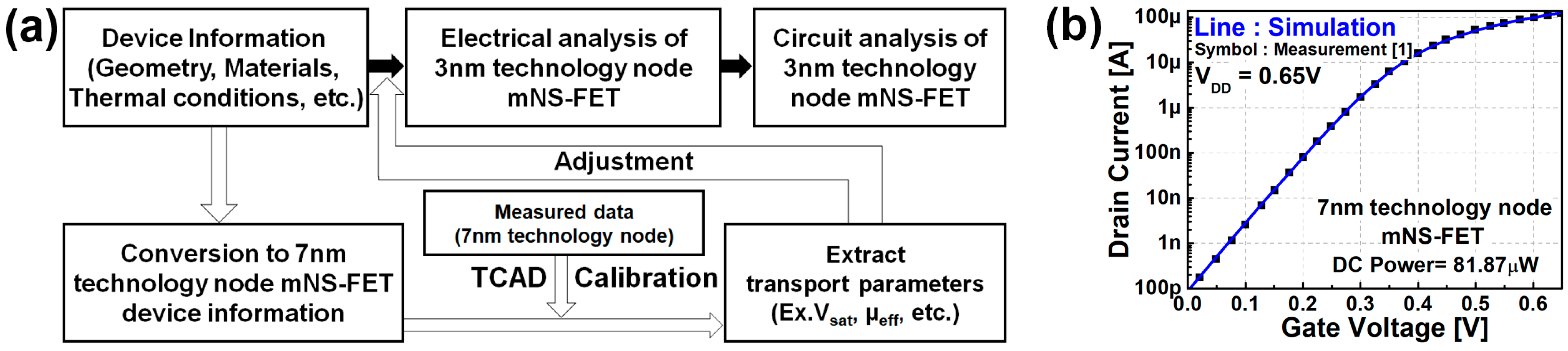
- To predict the subthreshold behavior accurately and apply the doping/temperature dependence, the Shockley–Read–Hall (SRH) recombination model (available in Synopsys Sentaurus Device) was included.
- The density gradient quantization model (eQuantumPotential) was included to describe the quantum confinement effect.
- The mobility model (PhuMob + High Field Saturation + Enormal) was utilized to consider the quantum effect, Coulomb scattering, and interfacial surface roughness scattering [10].
- The Lombardi mobility model was included to calculate the mobility degradation by remote phonon and Coulomb scatterings at the channel and insulator interface [11].
- A thin-layer mobility model was used to account for the thin channel thickness.
3. Conclusions
Author Contributions
Funding
Institutional Review Board Statement
Informed Consent Statement
Data Availability Statement
Acknowledgments
Conflicts of Interest
References
- Loubet, N.; Hook, T.; Montanini, P.; Yeung, C.-W.; Kanakasabapathy, S.; Guillom, M.; Yamashita, T.; Zhang, J.; Miao, X.; Wang, J.; et al. Stacked nanosheet gate-all-around transistor to enable scaling beyond FinFET. In Proceedings of the 2017 Symposium on VLSI Technology, Kyoto, Japan, 5–8 June 2017; IEEE: Piscataway, NJ, USA, 2017; pp. T230–T231. [Google Scholar]
- Bae, G.; Bae, D.-I.; Kang, M.; Hwang, S.M.; Kim, S.S.; Seo, B.; Kwon, T.Y.; Lee, T.J.; Moon, C.; Choi, Y.M.; et al. 3 nm GAA technology featuring multi-bridge-channel FET for low power and high performance applications. In Proceedings of the 2018 IEEE International Electron Devices Meeting (IEDM), San Francisco, CA, USA, 1–5 December 2018; IEEE: Piscataway, NJ, USA, 2018; pp. 28.7.1–28.7.4. [Google Scholar]
- Li, Q.; Bi, S.; Asare-Yeboah, K.; Na, J.; Liu, Y.; Jiang, C.; Song, J. High performance vertical resonant photo-effect-transistor with an all-around OLED-gate for ultra-electromagnetic stability. ACS Nano 2019, 13, 8425–8432. [Google Scholar] [CrossRef] [PubMed]
- Zhang, J.; Frougier, J.; Greene, A.; Miao, X.; Yu, L.; Vega, R.; Montanini, P.; Durfee, C.; Gaul, A.; Pancharatnam, S.; et al. Full bottom dielectric isolation to enable stacked nanosheet transistor for low power and high performance applications. In Proceedings of the 2019 IEEE International Electron Devices Meeting (IEDM), San Francisco, CA, USA, 7–11 December 2019; IEEE: Piscataway, NJ, USA, 2019; pp. 11.6.1–11.6.4. [Google Scholar]
- Yoon, J.-S.; Jeong, J.; Lee, S.; Baek, R.-H. Punch-through-stopper free nanosheet FETs with crescent inner-spacer and isolated source/drain. IEEE Access 2019, 7, 38593–38596. [Google Scholar] [CrossRef]
- Jegadheesan, V.; Sivasankaran, K.; Konar, A. Optimized Substrate for Improved Performance of Stacked Nanosheet Field-Effect Transistor. IEEE Trans. Electron. Devices 2020, 67, 4079–4084. [Google Scholar] [CrossRef]
- Myeong, I.; Song, I.; Kang, M.J.; Shin, H. Self-Heating and Electrothermal Properties of Advanced Sub-5-nm Node Nanoplate FET. IEEE Electron. Device Lett. 2020, 41, 977–980. [Google Scholar] [CrossRef]
- Seon, Y.; Chang, J.; Yoo, C.; Jeon, J. Device and circuit exploration of multi-nanosheet transistor for sub-3 nm technology node. Electronics 2021, 10, 180. [Google Scholar] [CrossRef]
- International Roadmap for Devices and Systems (IRDS™). 2020. Available online: https://irds.ieee.org/editions/2020 (accessed on 23 July 2020).
- Yoon, J.-S.; Jeong, J.; Lee, S.; Baek, R.-H. Multi-Vth Strategies of 7-nm node Nanosheet FETs With Limited Nanosheet Spacing. IEEE J. Electron. Devices Soc. 2018, 6, 861–865. [Google Scholar] [CrossRef]
- Son, D.; Myeong, I.; Kim, H.; Kang, M.; Jeon, J.; Shin, H. Analysis of electrothermal characteristics of GAA vertical nanoplate-shaped FETs. IEEE Trans. Electron. Devices 2018, 65, 3061–3064. [Google Scholar] [CrossRef]
- Dunga, M.V.; Lin, C.-H.; Niknejad, A.M.; Hu, C. BSIM-CMG: A compact model for multi-gate transistors. In FinFETs and Other Multi-Gate Transistors; Springer: Boston, MA, USA, 2008; pp. 113–153. [Google Scholar]
- Yakimets, D.; Garcia Bardon, M.; Jang, D.; Schuddinck, P.; Sherazi, Y.; Weckx, P.; Miyaguchi, K.; Parvais, B.; Raghavan, P.; Spessot, A.; et al. Power aware FinFET and lateral nanosheet FET targeting for 3nm CMOS technology. In Proceedings of the 2017 IEEE International Electron. Devices Meeting (IEDM), San Francisco, CA, USA, 2–6 December 2017; IEEE: Piscataway, NJ, USA, 2017; pp. 20.4.1–20.4.4. [Google Scholar]
- Martin, C.G.; Oruklu, E. Performance evaluation of FinFET pass-transistor full adders with BSIM-CMG model. In Proceedings of the 57th International Midwest Symposium on Circuits and Systems (MWSCAS), College Station, TX, USA, 3–6 August 2014; IEEE: Piscataway, NJ, USA, 2014; pp. 917–920. [Google Scholar]
- Seevinck, E.; List, F.J.; Lohstroh, J. Static-noise margin analysis of MOS SRAM cells. IEEE J. Solid-State Circuits 1987, 22, 748–754. [Google Scholar] [CrossRef] [Green Version]
- Venugopalan, S.; Joshi, V.; Zamudio, L.; Goldbach, M.; Burbach, G.; Van Bentum, R.; Balasubramanian, S. SRAM read current variability and its dependence on transistor statistics. In Proceedings of the IEEE 2013 Custom Integrated Circuits Conference, San Jose, CA, USA, 22–25 September 2013; IEEE: Piscataway, NJ, USA, 2013; pp. 1–4. [Google Scholar]
- Grossar, E.; Stucchi, M.; Maex, K.; Dehaene, W. Read stability and write-ability analysis of SRAM cells for nanometer technologies. IEEE J. Solid-State Circuits 2006, 41, 2577–2588. [Google Scholar] [CrossRef] [Green Version]


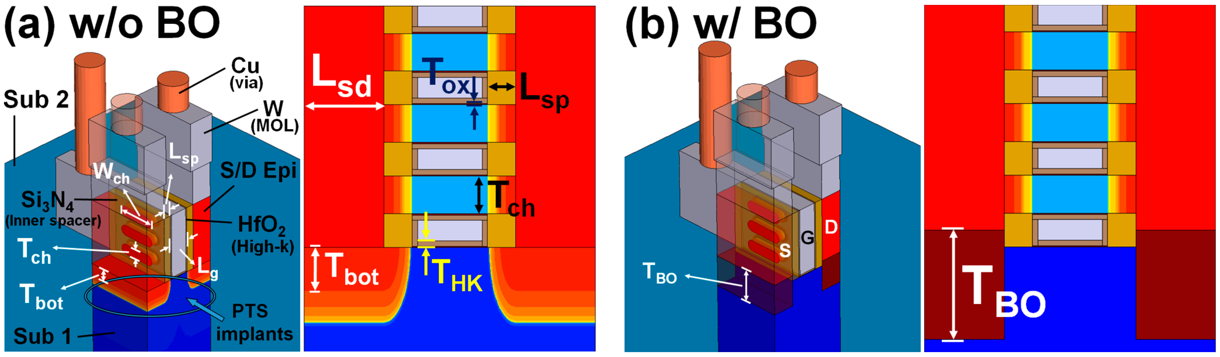
| Parameters | Values |
|---|---|
| Contacted poly-gate pitch (CPP) | 45 nm |
| Gate length (Lg) | 16 nm |
| Inner spacer length (Lsp) | 6 nm |
| Channel thickness (Tch) | 8 nm |
| Channel width (Wch) | 30 nm |
| Channel oxide thickness (Tox) | 0.3 nm |
| S/D length (Lsd) | 17 nm |
| Channel high-k thickness (THK) | 1.1 nm |
| Bottom oxide thickness (TBO) | 20 nm |
| S/D over-etching depth (Tbot) | 8.5 nm |
| Channel doping | 1 × 1017 cm−3 |
| S/D doping | 3 × 1020 cm−3 |
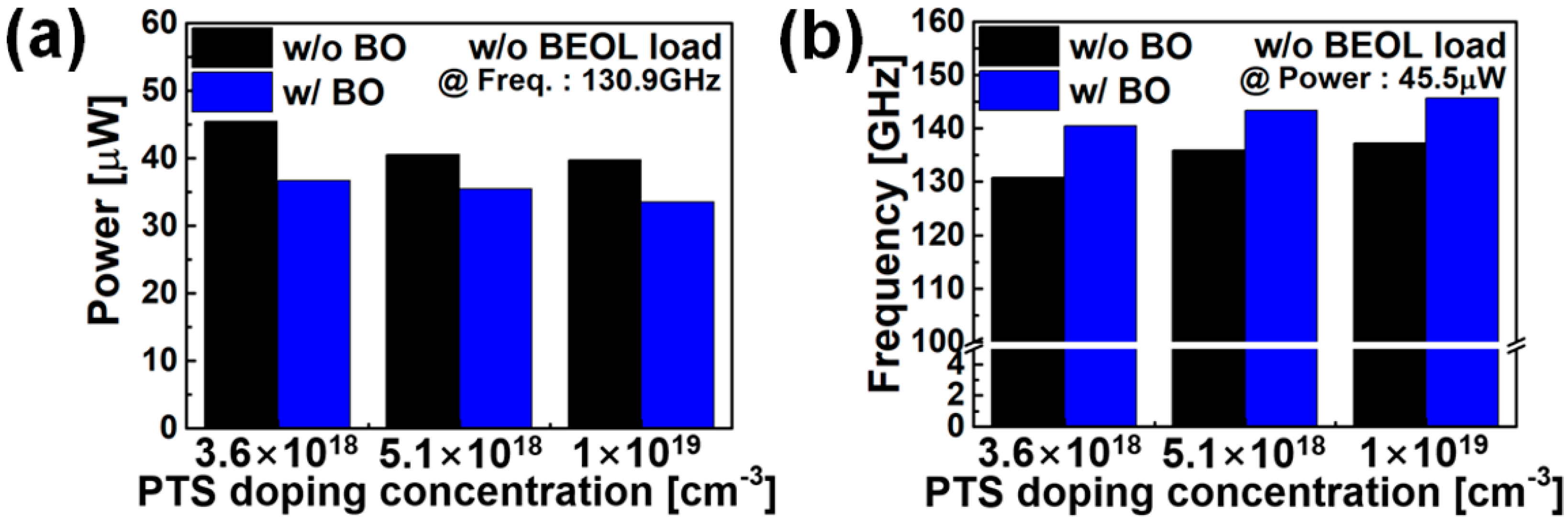
| PTS doping (upper of substrate 1) | 3.6 × 10¹⁸~1 × 1019 cm−3 |
| Substrate 2 doping | 1 × 1017 cm−3 |
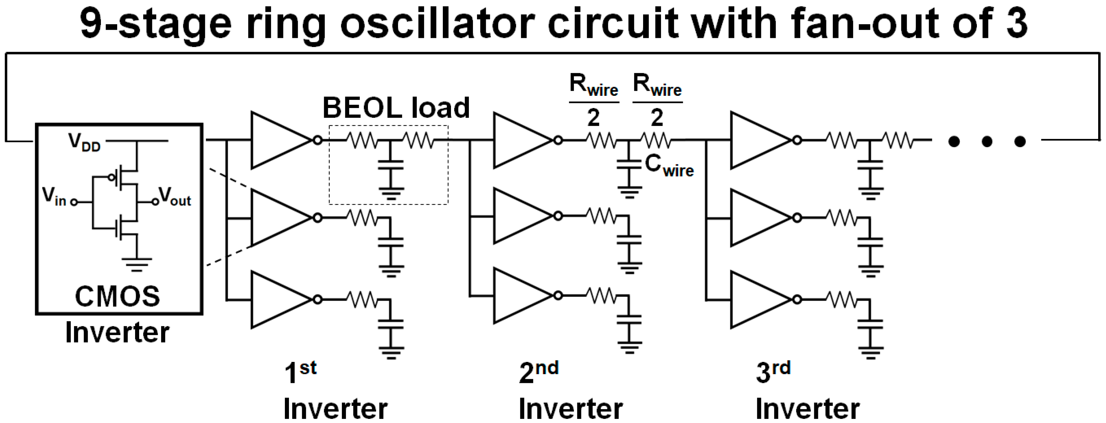
| w/o BO | w/BO | |||||
|---|---|---|---|---|---|---|
| Case type | Case 1 | Case 2 | Case 3 | Case 4 | Case 5 | Case 6 |
| Dynamic power [nW] | 627.6 | 690.4 | 693.4 | 619.7 | 587.1 | 600.8 |
| Delay [ps] | 61.72 | 54.39 | 55.36 | 53.02 | 51.33 | 52 |
| EDP [×10−27 J·s] | 46.8 | 45.3 | 46.1 | 40.1 | 36.8 | 38.3 |
| w/o BO | w/BO | |||||
|---|---|---|---|---|---|---|
| Case type | Case 1 | Case 2 | Case 3 | Case 4 | Case 5 | Case 6 |
| SNM [V] | 0.145 | 0.14 | 0.141 | 0.142 | 0.141 | 0.141 |
| IREAD [μA] | 113.6 | 134.8 | 131.1 | 128.7 | 128.7 | 129.5 |
| BWRM [V] | 0.217 | 0.242 | 0.244 | 0.243 | 0.243 | 0.243 |
Publisher’s Note: MDPI stays neutral with regard to jurisdictional claims in published maps and institutional affiliations. |
© 2022 by the authors. Licensee MDPI, Basel, Switzerland. This article is an open access article distributed under the terms and conditions of the Creative Commons Attribution (CC BY) license (https://creativecommons.org/licenses/by/4.0/).
Share and Cite
Yoo, C.; Chang, J.; Park, S.; Kim, H.; Jeon, J. Optimization of Gate-All-Around Device to Achieve High Performance and Low Power with Low Substrate Leakage. Nanomaterials 2022, 12, 591. https://doi.org/10.3390/nano12040591
Yoo C, Chang J, Park S, Kim H, Jeon J. Optimization of Gate-All-Around Device to Achieve High Performance and Low Power with Low Substrate Leakage. Nanomaterials. 2022; 12(4):591. https://doi.org/10.3390/nano12040591
Chicago/Turabian StyleYoo, Changhyun, Jeesoo Chang, Sugil Park, Hyungyeong Kim, and Jongwook Jeon. 2022. "Optimization of Gate-All-Around Device to Achieve High Performance and Low Power with Low Substrate Leakage" Nanomaterials 12, no. 4: 591. https://doi.org/10.3390/nano12040591