
Non-Volatile Programmable Ultra-Small Photonic Arbitrary Power Splitters

 ,
,
Abstract
:1. Introduction
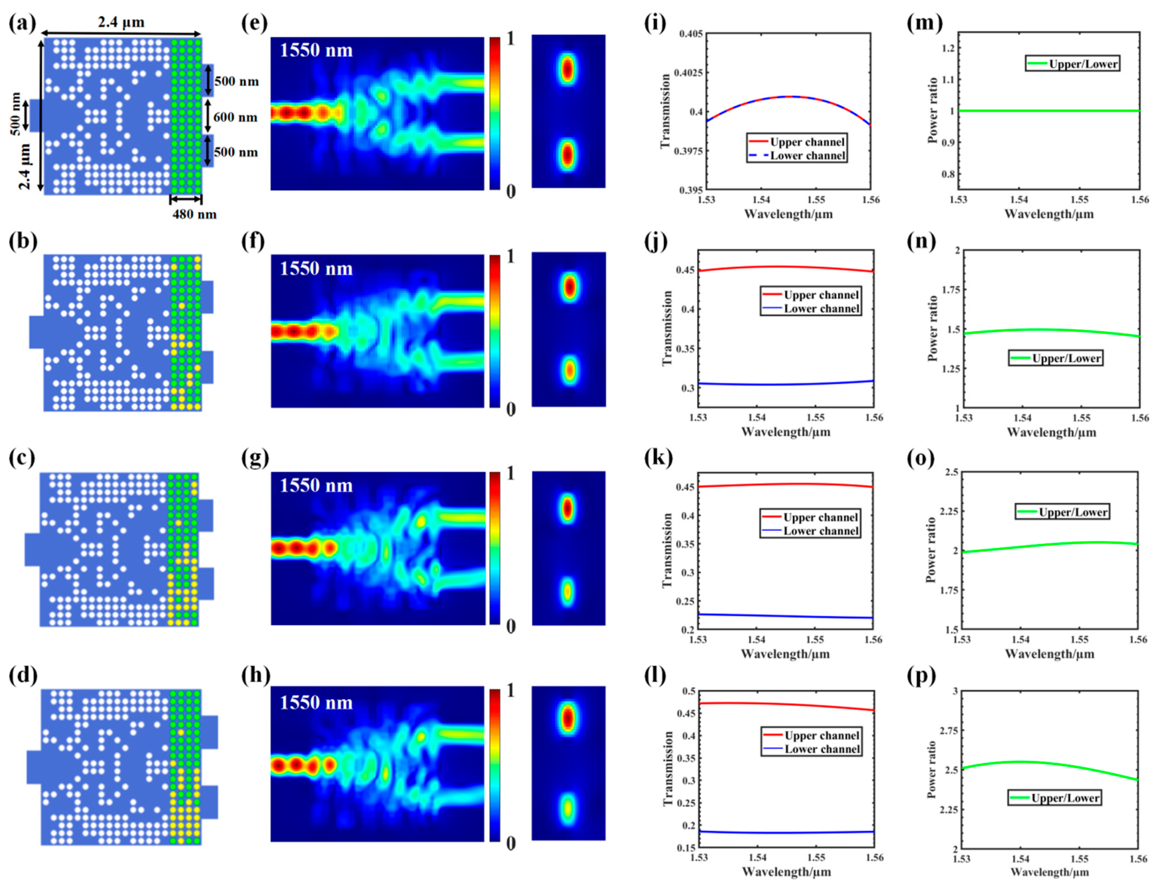
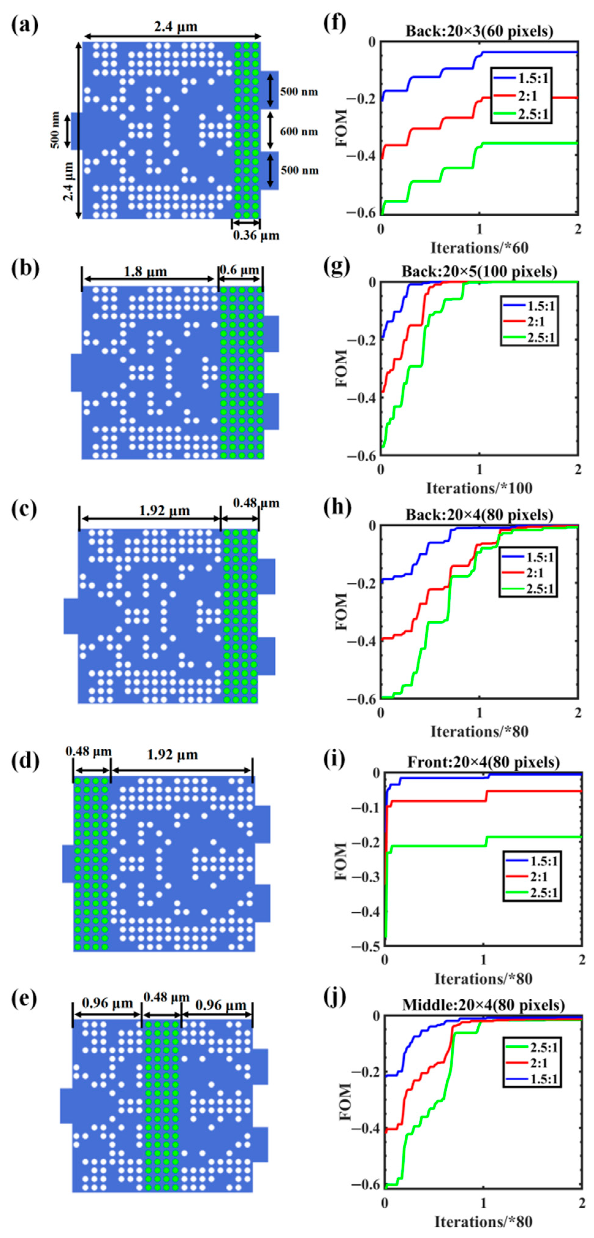
2. Principle and Simulation Results
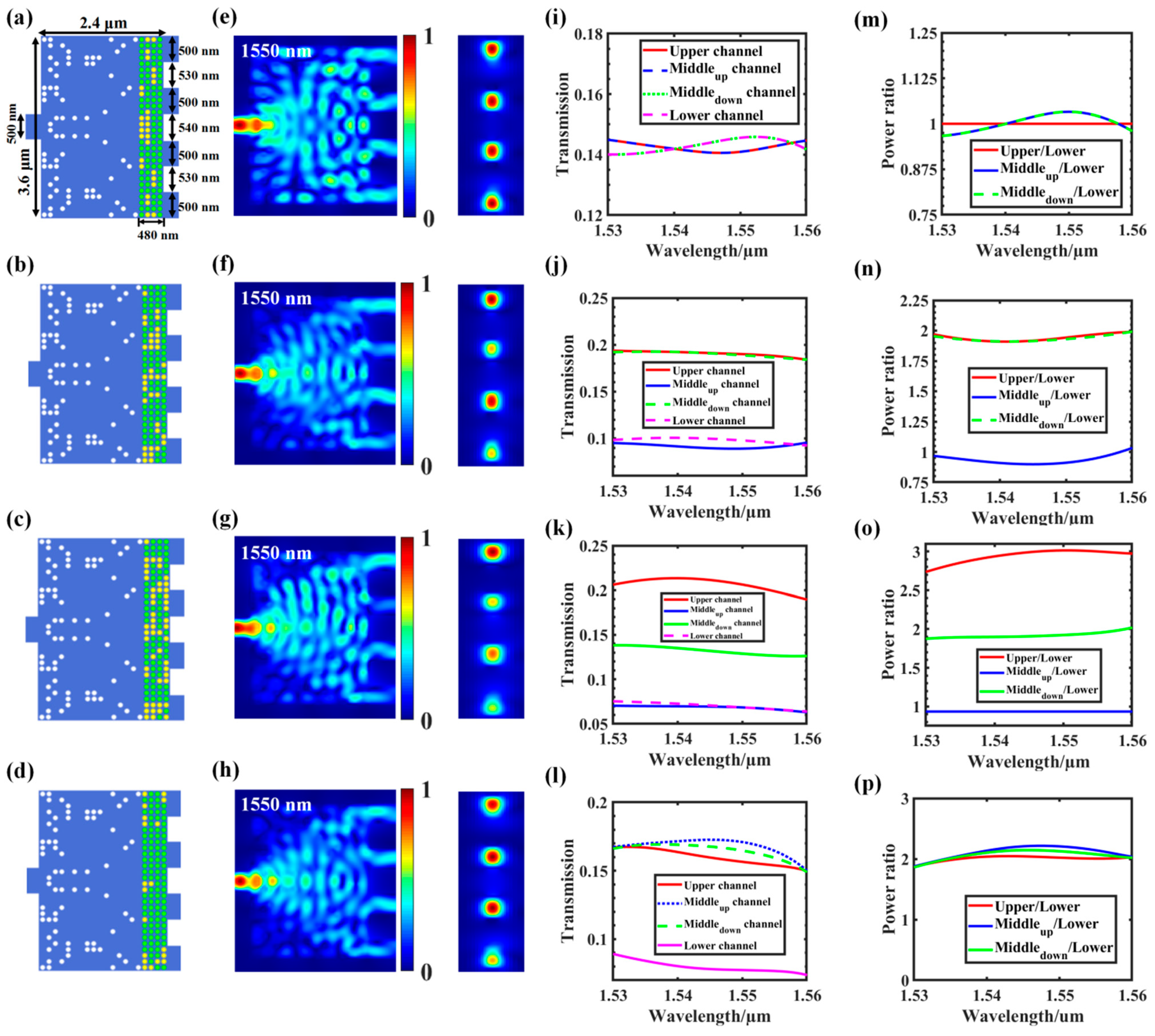
3. 1 × 3 and 1 × 4 Arbitrary Power Splitters
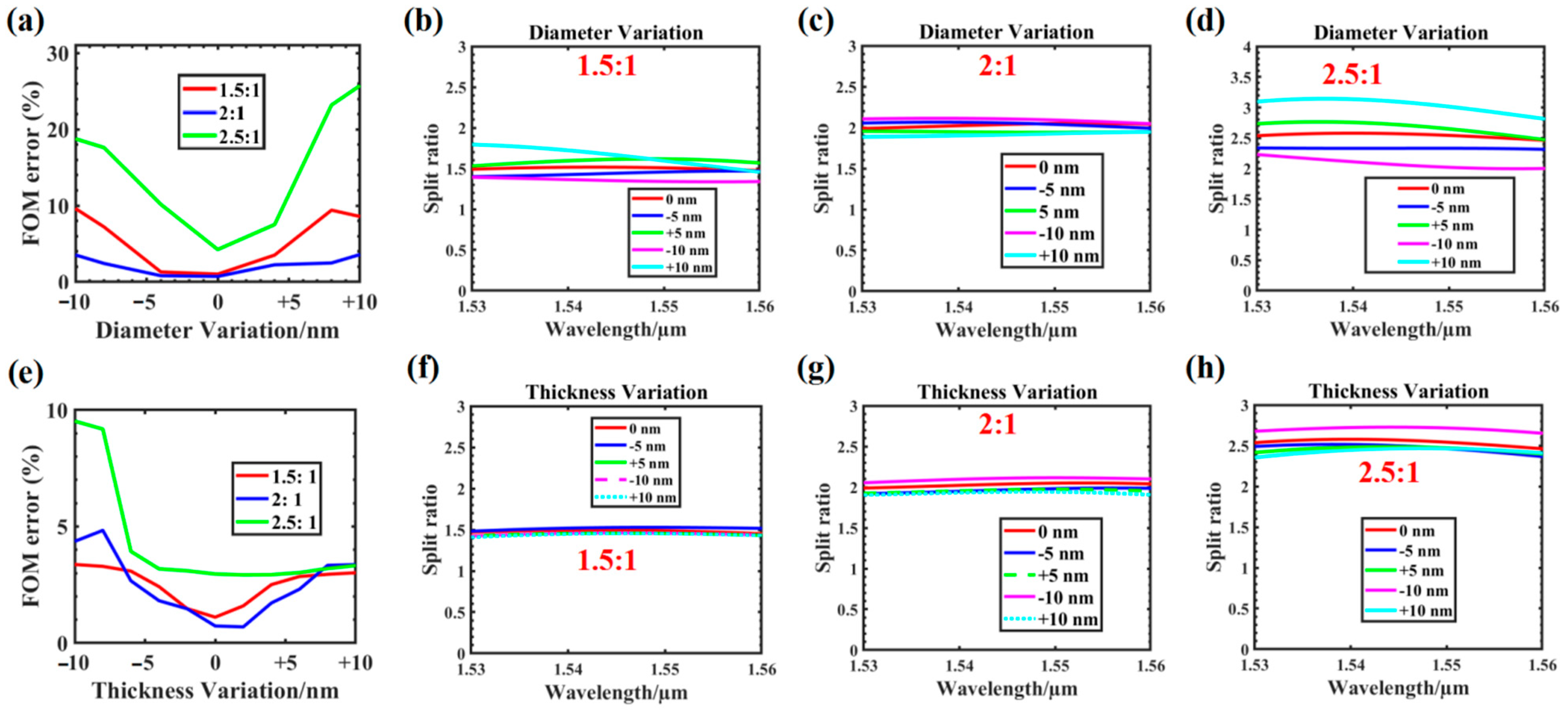
4. Tolerance to Fabrication Errors
5. Conclusions
Author Contributions
Funding
Institutional Review Board Statement
Informed Consent Statement
Data Availability Statement
Conflicts of Interest
References
- Pérez-López, D.; López, A.; DasMahapatra, P.; Capmany, J. Multipurpose self-configuration of programmable photonic circuits. Nat. Commun. 2020, 11, 6359. [Google Scholar] [CrossRef]
- Heßler, A.; Wahl, S.; Leuteritz, T.; Antonopoulos, A.; Stergianou, C.; Schön, C.-F.; Naumann, L.; Eicker, N.; Lewin, M.; Maß, T.W.W.; et al. In3SbTe2 as a programmable nanophotonics material platform for the infrared. Nat. Commun. 2021, 12, 924. [Google Scholar] [CrossRef]
- Li, L.; Cui, T.; Ji, W.; Liu, S.; Ding, J.; Wan, X.; Li, Y.; Jiang, M.; Qiu, C.; Zhang, S. Electromagnetic reprogrammable coding-metasurface holograms. Nat. Commun. 2017, 8, 197. [Google Scholar] [CrossRef] [PubMed] [Green Version]
- Wu, C.; Yu, H.; Lee, S.; Peng, R.; Takeuchi, I.; Li, M. Programmable phase-change metasurfaces on waveguides for multimode photonic convolutional neural network. Nat. Commun. 2021, 12, 96. [Google Scholar] [CrossRef]
- Peruzzo, A.; Laing, A.; Politi, A.; Rudolph, T.; O’Brien, J.L. Multimode quantum interference of photons in multiport integrated devices. Nat. Commun. 2011, 2, 224. [Google Scholar] [CrossRef] [Green Version]
- Wang, Q.; Pirro, P.; Verba, R.; Slavin, A.; Hillebrands, B.; Chumak, A.V. Reconfigurable nano-scale spin-wave directional coupler. Sci. Adv. 2017, 4, e1701517. [Google Scholar] [CrossRef] [Green Version]
- Gyger, S.; Zichi, J.; Schweickert, L.; Elshaari, A.W.; Steinhauer, S.; da Silva, S.F.C.; Rastelli, A.; Zwiller, V.; Jöns, K.D.; Errando-Herranz, C. Reconfigurable photonics with on-chip single-photon detectors. Nat. Commun. 2021, 12, 1408. [Google Scholar] [CrossRef]
- Ulrich, R.; Ankele, G. Self-imaging in homogeneous planar optical waveguides. Appl. Phys. Lett. 1975, 27, 337–339. [Google Scholar] [CrossRef]
- Li, Z.; Liu, Y.; Guan, H.; Han, W.; Li, Z. Ultra-compact low-loss 1×4 optical power splitter with splitting ratio of 1:2:4:8 based on two-stage cascaded MMI couplers. Opt. Lett. 2019, 44, 5622–5625. [Google Scholar] [CrossRef]
- Zanzi, A.; Brimont, A.; Griol, A.; Sanchis, P.; Marti, J. Compact and low-loss asymmetrical multimode interference splitter for power monitoring applications. Opt. Lett. 2016, 41, 227–229. [Google Scholar] [CrossRef]
- Deng, Q.; Liu, L.; Li, X.; Zhou, Z. Arbitrary-ratio 1 × 2 power splitter based on asymmetric multimode interference. Opt. Lett. 2014, 39, 5590–5593. [Google Scholar] [CrossRef] [Green Version]
- Azar, M.T.H.; Alipour-Banaei, H.; Zavvari, M. A High Efficiency Optical Power Splitter in a Y-Branch Photonic Crystal for DWDM Optical Communication Systems. Frequenz 2017, 72, 79–84. [Google Scholar] [CrossRef] [Green Version]
- Seif-Dargahi, H.; Zavvari, M.; Alipour-Banaei, H. Very compact photonic crystal resonant cavity for all optical filtering. J. Theor. Appl. Phys. 2014, 8, 183–188. [Google Scholar] [CrossRef] [Green Version]
- Tee, D.C.; Kambayashi, T.; Sandoghchi, S.R.; Tamchek, N.; Adikan, F.R.M. Efficient, wide angle, structure tuned 1 × 3 photonic crystal power splitter at 1550 nm for triple play applications. J. Lightwave Technol. 2012, 30, 2818–2823. [Google Scholar]
- Wang, K.; Ren, X.; Chang, W.; Lu, L.; Liu, D.; Zhang, M. Inverse design of digital nanophotonic devices using the adjoint method. Photonics Res. 2020, 8, 528. [Google Scholar] [CrossRef]
- Lu, L.; Liu, D.; Zhou, F.; Li, D.; Zhang, M. Inverse-designed single-step-etched colorless 3db couplers based on rie-lag-insensitive phc-like subwavelength structures. Opt. Lett. 2016, 41, 5051–5054. [Google Scholar] [CrossRef]
- Shen, B.; Wang, P.; Polson, R.; Menon, R. An integrated-nanophotonics polarization beamsplitter with 2.4 × 2.4 μm2 footprint. Nat. Photonics 2015, 9, 378–382. [Google Scholar] [CrossRef]
- Yu, Z.; Cui, H.; Sun, X. Genetically optimized on-chip wideband ultracompact reflectors and Fabry–Perot cavities. Photonics Res. 2017, 5, B15–B19. [Google Scholar] [CrossRef]
- Ma, W.; Cheng, F.; Liu, Y. Deep-Learning-Enabled On-Demand Design of Chiral Metamaterials. ACS Nano 2018, 12, 6326–6334. [Google Scholar] [CrossRef]
- Xu, K.; Liu, L.; Wen, X.; Sun, W.; Zhang, N.; Yi, N.; Sun, S.; Xiao, S.; Song, Q. Integrated photonic power divider with arbitrary power ratios. Opt. Lett. 2017, 42, 855–858. [Google Scholar] [CrossRef] [Green Version]
- Tahersima, M.H.; Kojima, K.; Koike-Akino, T.; Jha, D.; Wang, B.; Lin, C.; Parsons, K. Deep Neural Network Inverse Design of Integrated Photonic Power Splitters. Sci. Rep. 2019, 9, 1368. [Google Scholar] [CrossRef]
- Huang, J.; Ma, H.; Chen, D.; Yuan, H.; Zhang, J.; Li, Z.; Han, J.; Wu, J.; Yang, J. Digital nanophotonics: The highway to the integration of subwavelength-scale photonics: Ultra-compact, multi-function nanophotonic design based on computational inverse design. Nanophotonics 2021, 10, 1011–1030. [Google Scholar] [CrossRef]
- Liu, Y.; Xu, K.; Wang, S.; Shen, W.; Xie, H.; Wang, Y.; Xiao, S.; Yao, Y.; Du, J.; He, Z.; et al. Arbitrarily routed mode-division multiplexed photonic circuits for dense integration. Nat. Commun. 2019, 10, 3263. [Google Scholar] [CrossRef] [Green Version]
- Piggott, A.Y.; Lu, J.; Lagoudakis, K.G.; Petykiewicz, J.; Babinec, T.M.; Vuckovic, J. Inverse design and demonstration of a compact and broadband on-chip wavelength demultiplexer. Nat. Photonics 2015, 9, 374–377. [Google Scholar] [CrossRef] [Green Version]
- Chang, W.; Lu, L.; Ren, X.; Li, D.; Pan, Z.; Cheng, M.; Liu, D.; Zhang, M. Ultracompact dual-mode waveguide crossing based on subwavelength multimode-interference couplers. Photonics Res. 2018, 6, 660–665. [Google Scholar] [CrossRef]
- Huang, J.; Yang, J.; Chen, D.; Bai, W.; Han, J.; Zhang, Z.; Zhang, J.; He, X.; Han, Y.; Liang, L. Implementation of on-chip multi-channel focusing wavelength demultiplexer with regularized digital metamaterials. Nanophotonics 2019, 9, 159–166. [Google Scholar] [CrossRef]
- Meng, Y.; Chen, Y.; Lu, L.; Ding, Y.; Cusano, A.; Fan, J.A.; Hu, Q.; Wang, K.; Xie, Z.; Liu, Z.; et al. Optical meta-waveguides for integrated photonics and beyond. Light Sci. Appl. 2021, 10, 235. [Google Scholar] [CrossRef]
- Tian, Y.; Qiu, J.; Yu, M.; Huang, Z.; Qiao, Y.Y.; Dong, Z.; Wu, J. Broadband 1 × 3 Couplers With Variable Splitting Ratio Using Cascaded Step-Size MMI. IEEE Photonics J. 2018, 10, 1–8. [Google Scholar] [CrossRef]
- Wuttig, M.; Bhaskaran, H.; Taubner, T. Phase-change materials for non-volatile photonic applications. Nat. Photonics 2017, 11, 465–476. [Google Scholar] [CrossRef]
- Waldecker, L.; Miller, T.; Rudé, M.; Bertoni, R.; Osmond, J.; Pruneri, V.; Simpson, R.; Ernstorfer, R.; Wall, S. Time-domain separation of optical properties from structural transitions in resonantly bonded materials. Nat. Mater. 2015, 14, 991–995. [Google Scholar] [CrossRef] [PubMed]
- Zhang, C.; Zhang, M.; Xie, Y.; Shi, Y.; Kumar, R.; Panepucci, R.R.; Dai, D. Wavelength-selective 2 × 2 optical switch based on a Ge2Sb2Te5-assisted microring. Photonics Res. 2020, 8, 1171. [Google Scholar] [CrossRef]
- Xu, P.; Zheng, J.; Doylend, J.; Majumdar, A. Low-loss and broadband non-volatile phasechange directional coupler switches. ACS Photonics 2019, 6, 553–557. [Google Scholar] [CrossRef] [Green Version]
- Rude, M.; Pello, J.; Simpson, R.E.; Osmond, J.; Roelkens, G.; Tol, J.; Pruneri, V. Optical switching at 1.55 μm in silicon racetrack resonators using phase change materials. Appl. Phys. Lett. 2013, 103, 325. [Google Scholar] [CrossRef] [Green Version]
- Tanaka, D.; Shoji, Y.; Kuwahara, M.; Wang, X.; Kintaka, K.; Kawashima, H.; Toyosaki, T.; Ikuma, Y.; Tsuda, H. Ultra-small, self-holding, optical gate switch using Ge2Sb2Te5 with a multi-mode Si waveguide. Opt. Express 2012, 20, 10283. [Google Scholar] [CrossRef]
- Zhang, Z.; Yang, J.; Bai, W.; Han, Y.; He, X.; Huang, J.; Chen, D.; Xu, S.; Xie, W. All-optical switch and logic gates based on hybrid silicon-Ge2Sb2Te5 metasurfaces. Appl. Opt. 2019, 58, 7392–7396. [Google Scholar] [CrossRef] [Green Version]
- Gholipour, B.; Zhang, J.; MacDonald, K.F.; Hewak, D.W.; Zheludev, N.I. An All-Optical, Non-volatile, Bidirectional, Phase-Change Meta-Switch. Adv. Mater. 2013, 25, 3050–3054. [Google Scholar] [CrossRef]
- Wang, Q.; Rogers, E.; Gholipour, B.; Wang, C.-M.; Yuan, G.; Teng, J.; Zheludev, N. Optically reconfigurable metasurfaces and photonic devices based on phase change materials. Nat. Photonics 2015, 10, 60–65. [Google Scholar] [CrossRef] [Green Version]
- Ríos, C.; Stegmaier, M.; Hosseini, P.; Wang, D.; Scherer, T.; Wright, C.D.; Bhaskaran, H.; Pernice, W.H.P. Integrated all-photonic non-volatile multi-level memory. Nat. Photonics 2015, 9, 725–732. [Google Scholar] [CrossRef] [Green Version]
- Rios, C.; Hosseini, P.; Wright, C.D.; Bhaskaran, H.; Pernice, W.H.P. On-Chip Photonic Memory Elements Employing Phase-Change Materials. Adv. Mater. 2013, 26, 1372–1377. [Google Scholar] [CrossRef] [Green Version]
- Feldmann, J.; Stegmaier, M.; Gruhler, N.; Ríos, C.; Bhaskaran, H.; Wright, C.D.; Pernice, W.H.P. Calculating with light using a chip-scale all-optical abacus. Nat. Commun. 2017, 8, 1256. [Google Scholar] [CrossRef] [Green Version]
- Kato, K.; Kuwahara, M.; Kawashima, H.; Tsuruoka, T.; Tsuda, H. Current-driven phase-change optical gate switch using indium–tin-oxide heater. Appl. Phys. Express 2017, 10, 072201. [Google Scholar] [CrossRef]
- Zhang, Y.; Li, J.; Chou, J.B.; Fang, Z.; Yadav, A.; Lin, H.; Du, Q.; Michon, J.; Han, Z.; Huang, Y. Broadband Transparent Optical Phase Change Materials. In CLEO: Applications and Technology; Optical Society of America: Washington, DC, USA, 2017; p. JTh5C-4. [Google Scholar]
- Zhang, Y.; Chou, J.B.; Li, J.; Li, H.; Du, Q.; Yadav, A.; Zhou, S.; Shalaginov, M.Y.; Fang, Z.; Zhong, H.; et al. Broadband transparent optical phase change materials for high-performance nonvolatile photonics. Nat. Commun. 2019, 10, 4279. [Google Scholar] [CrossRef] [PubMed]
- De Leonardis, F.; Soref, R.A.; Passaro, V.M.N.; Zhang, Y.; Hu, J. Broadband Electro-Optical Crossbar Switches Using Low-Loss Ge2Sb2Se4Te1 Phase Change Material. J. Lightwave Technol. 2019, 37, 3183–3191. [Google Scholar] [CrossRef]
- Zhang, Q.; Zhang, Y.; Li, J.; Soref, R.; Gu, T.; Hu, J. Broadband nonvolatile photonic switching based on optical phase change materials: Beyond the classical figure-of-merit. Opt. Lett. 2017, 43, 94–97. [Google Scholar] [CrossRef] [PubMed]
- Zhang, Y.; Zhang, Q.; Ríos, C.; Shalaginov, M.Y.; Chou, J.B.; Roberts, C.; Miller, P.; Robinson, P.; Liberman, V.; Kang, M.; et al. Transient Tap Couplers for Wafer-Level Photonic Testing Based on Optical Phase Change Materials. ACS Photonics 2021, 8, 1903–1908. [Google Scholar] [CrossRef]
- Chen, H.; Jia, H.; Yang, J.; Tian, Y.; Wang, T. Ultra-compact switchable mode converter based on silicon and optical phase change material hybrid metastructure. Opt. Commun. 2020, 473, 125889. [Google Scholar] [CrossRef]
- Ma, H.; Yang, J.; Huang, J.; Zhang, Z.; Zhang, K. Inverse-designed single-mode and multi-mode nanophotonic waveguide switches based on hybrid silicon-Ge2Sb2Te5 platform. Results Phys. 2021, 26, 104384. [Google Scholar] [CrossRef]
- Chen, H.; Jia, H.; Wang, T.; Tian, Y.; Yang, J. Broadband Nonvolatile Tunable Mode-Order Converter Based on Silicon and Optical Phase Change Materials Hybrid Meta-Structure. J. Lightwave Technol. 2020, 38, 1874–1879. [Google Scholar] [CrossRef]
- Delaney, M.; Zeimpekis, I.; Du, H.; Yan, X.; Banakar, M.; Thomson, D.J.; Hewak, D.W.; Muskens, O.L. Nonvolatile programmable silicon photonics using an ultralow-loss Sb2Se3 phase change material. Sci. Adv. 2021, 7, eabg3500. [Google Scholar] [CrossRef]
- Meng, C.; Qiu, J.; Tian, Y.; Ye, Z.; Wu, J. A broadband compact 1 × 3 power splitter designed with inverse design method. In Proceedings of the 2016 15th International Conference on Optical Communications and Networks (ICOCN), Hangzhou, China, 24–27 September 2016; pp. 1–3. [Google Scholar]
- Xie, H.; Liu, Y.; Sun, W.; Wang, Y.; Xu, K.; Du, J.; He, Z.; Song, Q. Inversely Designed 1 × 4 Power Splitter With Arbitrary Ratios at 2-μm Spectral Band. IEEE Photonics J. 2018, 10, 1–6. [Google Scholar] [CrossRef]


| Power Ratio | True Value | Distribution of GSST |
|---|---|---|
| 1:1 | 0 0 0 0 0 0 0 0 0 0 0 0 0 0 0 0 0 0 0 0 | 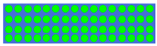 |
| 0 0 0 0 0 0 0 0 0 0 0 0 0 0 0 0 0 0 0 0 | ||
| 0 0 0 0 0 0 0 0 0 0 0 0 0 0 0 0 0 0 0 0 | ||
| 0 0 0 0 0 0 0 0 0 0 0 0 0 0 0 0 0 0 0 0 | ||
| 1.5:1 | 0 1 0 0 0 0 0 0 0 0 1 1 1 0 0 0 0 1 0 1 | 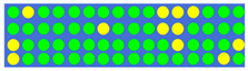 |
| 0 0 0 0 0 0 1 0 0 0 1 1 0 0 0 0 0 1 1 1 | ||
| 1 0 0 0 0 0 0 0 0 0 0 1 0 0 0 1 1 0 0 1 | ||
| 1 0 0 0 0 0 0 0 0 0 0 0 0 0 1 0 0 0 0 1 | ||
| 2:1 | 0 1 1 0 0 0 0 0 0 0 0 1 1 1 1 1 1 1 0 0 |  |
| 0 0 0 0 0 0 0 0 0 1 1 1 0 0 0 1 1 1 0 1 | ||
| 0 0 0 0 0 0 1 0 0 0 0 1 0 0 0 1 0 1 0 1 | ||
| 0 0 0 0 0 0 0 0 0 0 0 0 0 1 1 1 1 1 1 1 | ||
| 2.5:1 | 0 0 0 0 0 0 0 0 0 0 1 1 1 1 0 1 1 1 1 0 | 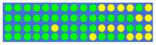 |
| 0 0 0 0 0 0 0 0 0 0 0 0 0 0 1 1 1 1 1 0 | ||
| 0 0 0 0 0 1 0 0 0 0 1 1 1 0 0 1 1 1 1 1 | ||
| 0 0 0 0 0 0 0 0 0 1 0 0 0 1 1 1 1 1 1 0 |
| Power Ratio | True Value | Distribution of GSST |
|---|---|---|
| 1:1:1 | 0 0 0 0 0 0 0 0 0 0 0 0 0 0 0 0 0 0 0 0 | 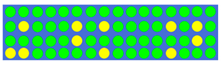 |
| 0 1 0 0 0 1 0 1 0 0 0 0 1 0 1 0 0 0 1 0 | ||
| 0 0 0 0 0 1 0 0 0 0 0 0 0 0 1 0 0 0 0 0 | ||
| 1 1 0 0 0 0 0 1 0 0 0 0 1 0 0 0 0 0 1 1 | ||
| 2:1.5:1 | 0 0 0 0 0 0 0 0 0 0 0 0 0 0 1 0 0 0 0 0 |  |
| 0 0 0 0 0 0 0 1 0 0 1 0 0 0 0 0 1 1 1 0 | ||
| 0 1 0 0 0 0 0 1 0 0 0 1 1 1 1 1 1 0 0 1 | ||
| 0 0 0 0 0 0 0 1 0 0 0 0 0 0 1 1 1 1 1 1 | ||
| 2:1:1 | 0 0 0 0 0 0 0 0 0 1 0 0 0 1 1 1 0 0 0 1 | 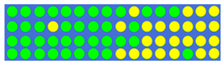 |
| 0 0 0 1 0 0 0 0 1 0 1 1 1 1 1 1 1 1 1 0 | ||
| 0 0 0 0 0 0 0 0 0 0 1 1 1 1 1 1 1 0 0 1 | ||
| 0 0 0 0 0 0 0 0 1 1 1 1 1 0 1 1 1 1 1 1 | ||
| 2:1:2 | 0 0 0 0 0 0 0 0 0 0 0 1 1 0 0 0 0 0 0 0 | 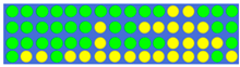 |
| 0 0 0 0 0 0 1 0 0 1 1 1 1 1 0 0 1 0 1 0 | ||
| 0 0 0 0 0 0 1 0 0 0 0 1 1 1 1 0 1 0 0 0 | ||
| 0 1 1 0 1 1 1 1 1 1 1 1 1 1 0 1 0 0 1 0 |
| Power Ratio | True Value | Distribution of GSST |
|---|---|---|
| 1:1:1:1 | 0 0 0 0 0 0 0 0 0 0 0 0 0 0 0 0 0 0 0 0 0 0 0 0 0 0 0 0 0 0 | 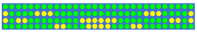 |
| 1 0 0 0 0 1 1 1 0 0 0 0 0 0 0 0 0 0 0 0 0 0 1 1 1 0 0 0 0 1 | ||
| 1 0 1 1 0 0 0 0 0 0 0 0 1 1 1 1 1 1 0 0 0 0 0 0 0 0 1 1 0 1 | ||
| 0 0 0 0 0 0 0 0 1 1 0 0 0 1 1 1 1 0 0 0 1 1 0 0 0 0 0 0 0 0 | ||
| 2:1:2:1 | 0 0 0 0 0 0 0 0 0 0 0 0 0 0 0 1 0 0 0 0 0 0 0 0 0 1 1 0 0 0 |  |
| 0 0 0 0 1 1 0 1 1 1 1 0 0 1 0 1 0 0 1 0 0 0 0 1 1 0 0 1 0 0 | ||
| 0 0 0 0 0 0 0 0 1 1 1 0 0 0 1 1 0 0 1 0 0 0 0 0 0 0 0 1 1 1 | ||
| 0 1 0 0 0 1 1 0 0 0 1 0 0 0 0 1 1 1 0 1 0 0 0 0 0 0 0 1 1 1 | ||
| 3:1:2:1 | 0 0 0 0 0 0 1 1 1 1 1 1 0 1 1 0 1 0 0 0 1 1 1 1 0 0 0 1 0 1 |  |
| 0 0 0 1 1 0 0 1 1 0 0 0 0 0 0 1 0 0 1 0 0 0 0 1 0 0 0 1 1 0 | ||
| 0 0 0 1 0 0 0 0 1 1 1 0 1 1 1 1 0 0 0 1 0 0 0 0 0 0 0 1 1 1 | ||
| 1 0 0 1 1 1 1 0 0 0 0 0 0 0 1 1 1 0 0 0 0 1 1 0 0 0 0 1 1 1 | ||
| 2:2:2:1 | 1 1 0 0 0 0 0 0 0 0 0 0 0 0 0 0 0 0 0 0 0 0 0 0 0 0 1 1 1 0 | 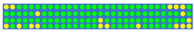 |
| 0 0 0 0 0 1 0 0 0 0 0 0 0 0 0 0 0 0 0 0 0 0 0 0 0 0 0 0 1 0 | ||
| 0 0 0 0 0 0 0 0 0 0 0 0 0 0 0 1 0 0 0 0 0 0 0 0 0 0 0 0 0 1 | ||
| 1 0 1 0 1 1 0 0 0 0 0 0 0 0 0 1 1 0 0 0 0 1 0 0 0 0 0 1 1 1 |
| Refs. | [9] | [20] | [51] | This Work |
|---|---|---|---|---|
| Footprint | 124 × 6.4 µm2 | 3.6 × 3.6 µm2 | 2.8 × 2.8 µm2 | 2.4 × 2.4 µm2, 2.4 × 3.6 µm2 |
| Dimension of the input/output waveguide | 1.6 µm | 480 nm | 500 nm | 500 nm |
| Containing O-PCM | No | No | No | Yes (Ge2Sb2Se4Te1) |
| Operating bandwidth | 1530–1570 nm | 1530–1560 nm | 1500–1600 nm | 1530–1560 nm |
| Maximum number of channels | 4 | 3 | 3 | 4 |
| Design technology | Forward design | Inverse design | Inverse design | Inverse design |
| Non-volatile | No | No | No | Yes |
| Tunability | No | No | No | Yes |
| Programmable | No | No | No | Yes |
| Error analysis | No | No | No | Yes |
| Origin of results | Experiment and simulation | Experiment and simulation | Simulation | Simulation |
Publisher’s Note: MDPI stays neutral with regard to jurisdictional claims in published maps and institutional affiliations. |
© 2022 by the authors. Licensee MDPI, Basel, Switzerland. This article is an open access article distributed under the terms and conditions of the Creative Commons Attribution (CC BY) license (https://creativecommons.org/licenses/by/4.0/).
Share and Cite
Yuan, H.; Wu, J.; Zhang, J.; Pu, X.; Zhang, Z.; Yu, Y.; Yang, J. Non-Volatile Programmable Ultra-Small Photonic Arbitrary Power Splitters. Nanomaterials 2022, 12, 669. https://doi.org/10.3390/nano12040669
Yuan H, Wu J, Zhang J, Pu X, Zhang Z, Yu Y, Yang J. Non-Volatile Programmable Ultra-Small Photonic Arbitrary Power Splitters. Nanomaterials. 2022; 12(4):669. https://doi.org/10.3390/nano12040669
Chicago/Turabian StyleYuan, Huan, Jiagui Wu, Jinping Zhang, Xun Pu, Zhenfu Zhang, Yang Yu, and Junbo Yang. 2022. "Non-Volatile Programmable Ultra-Small Photonic Arbitrary Power Splitters" Nanomaterials 12, no. 4: 669. https://doi.org/10.3390/nano12040669