
Functional Devices from Bottom-Up Silicon Nanowires: A Review

 and
and
Abstract
: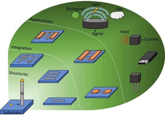
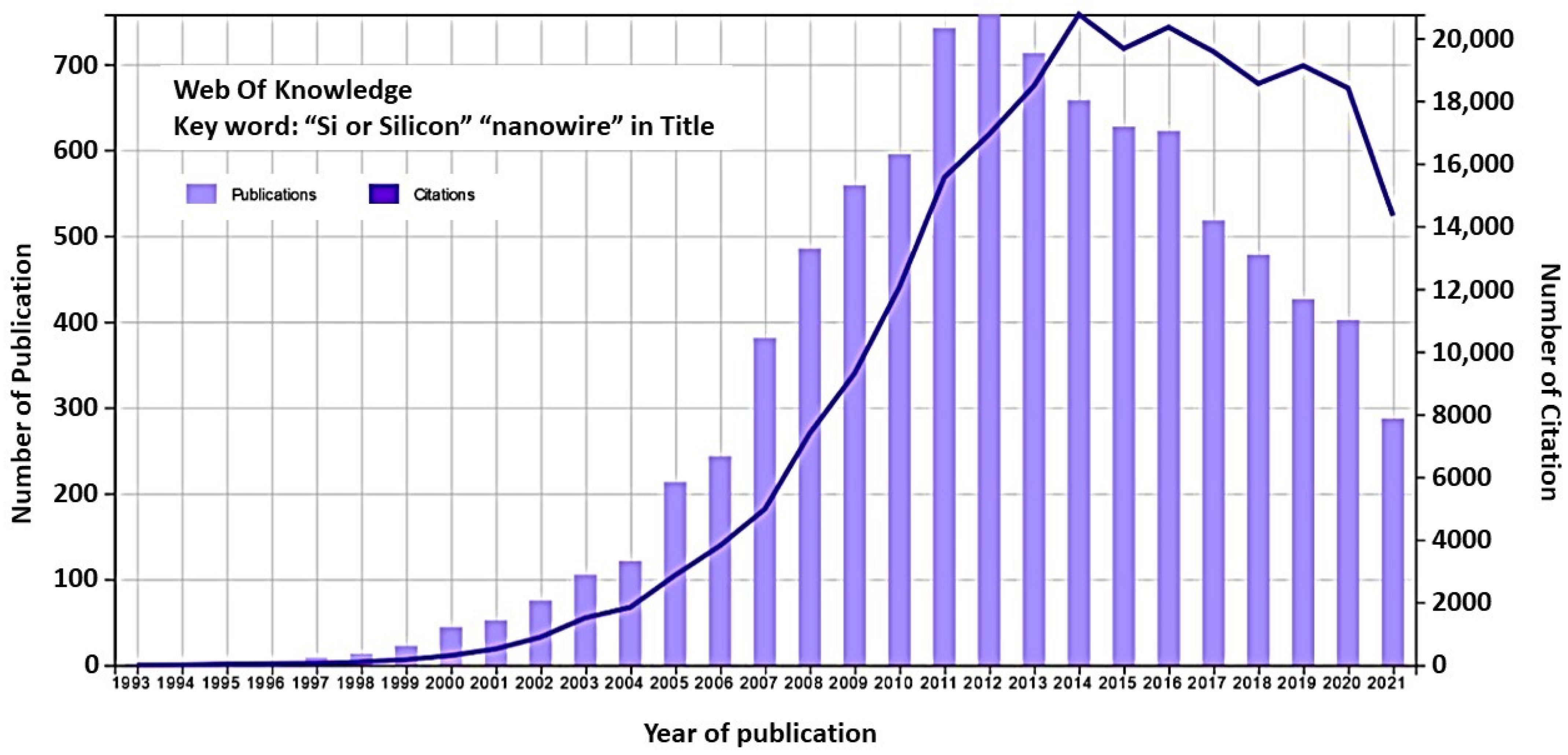
1. Introduction
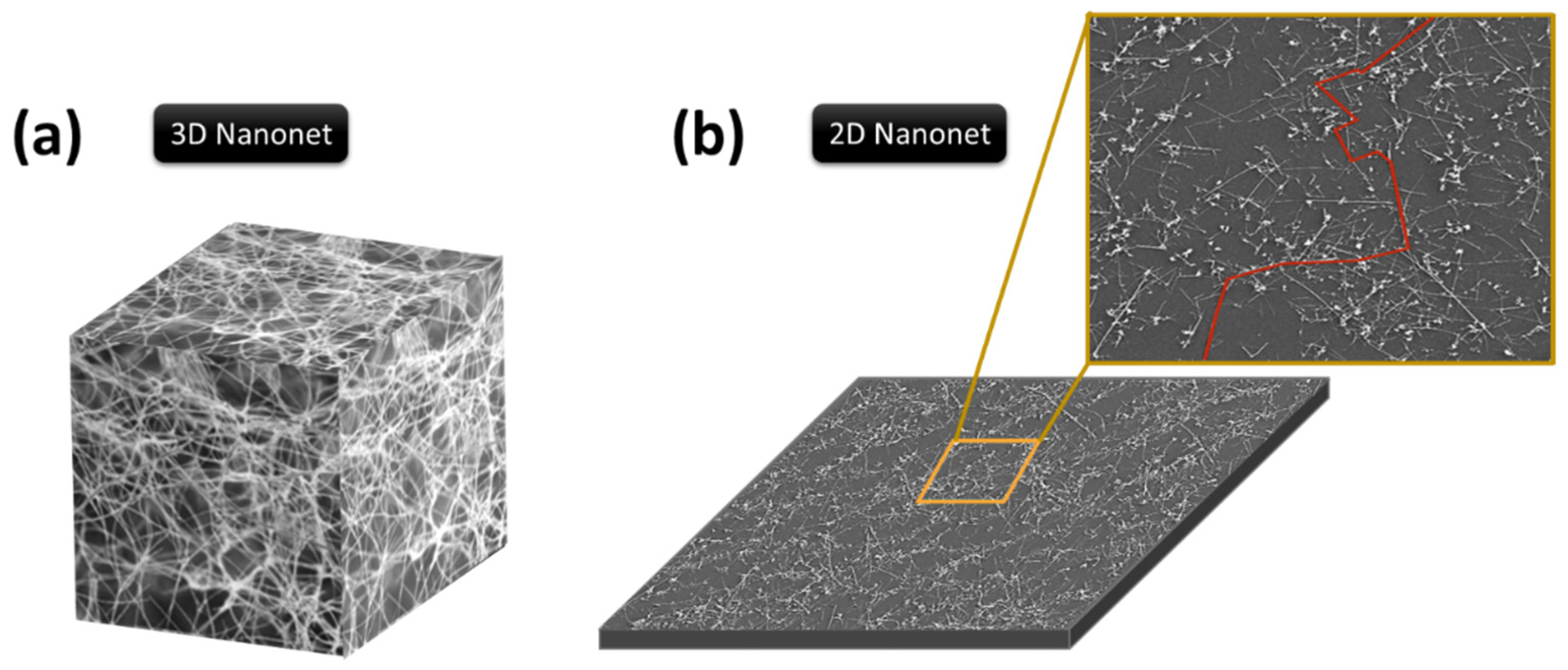
2. From Nanowire-Based to Nanonet-Based Silicon Devices
3. Silicon Nanowire Properties
3.1. Mechanical Properties
3.2. Electrical Properties
3.3. Surface Chemistry
3.4. Optical Properties
3.5. Thermal Properties
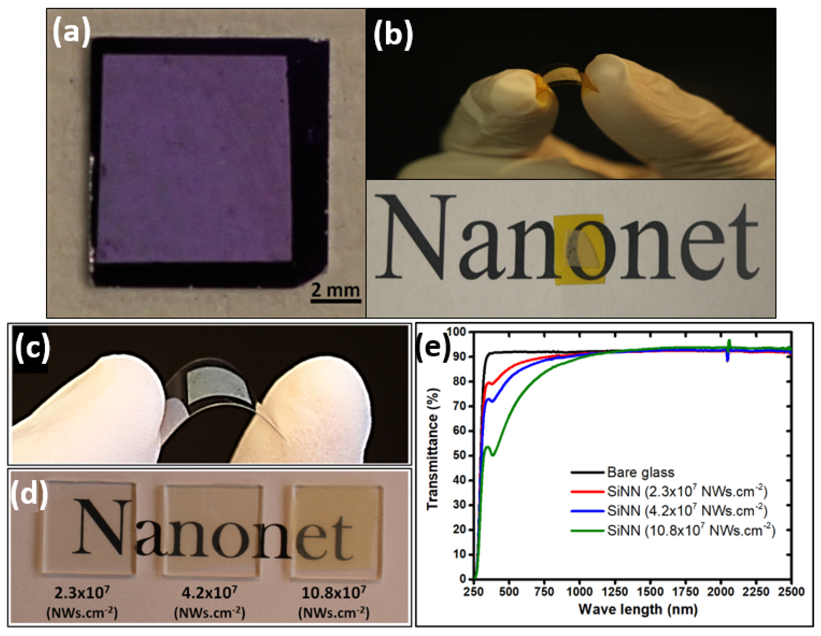
4. Silicon Nanonet Properties
4.1. Electrical Conductivity
4.2. Porosity and Optical Transparency
4.3. Mechanical Strength and Flexibility
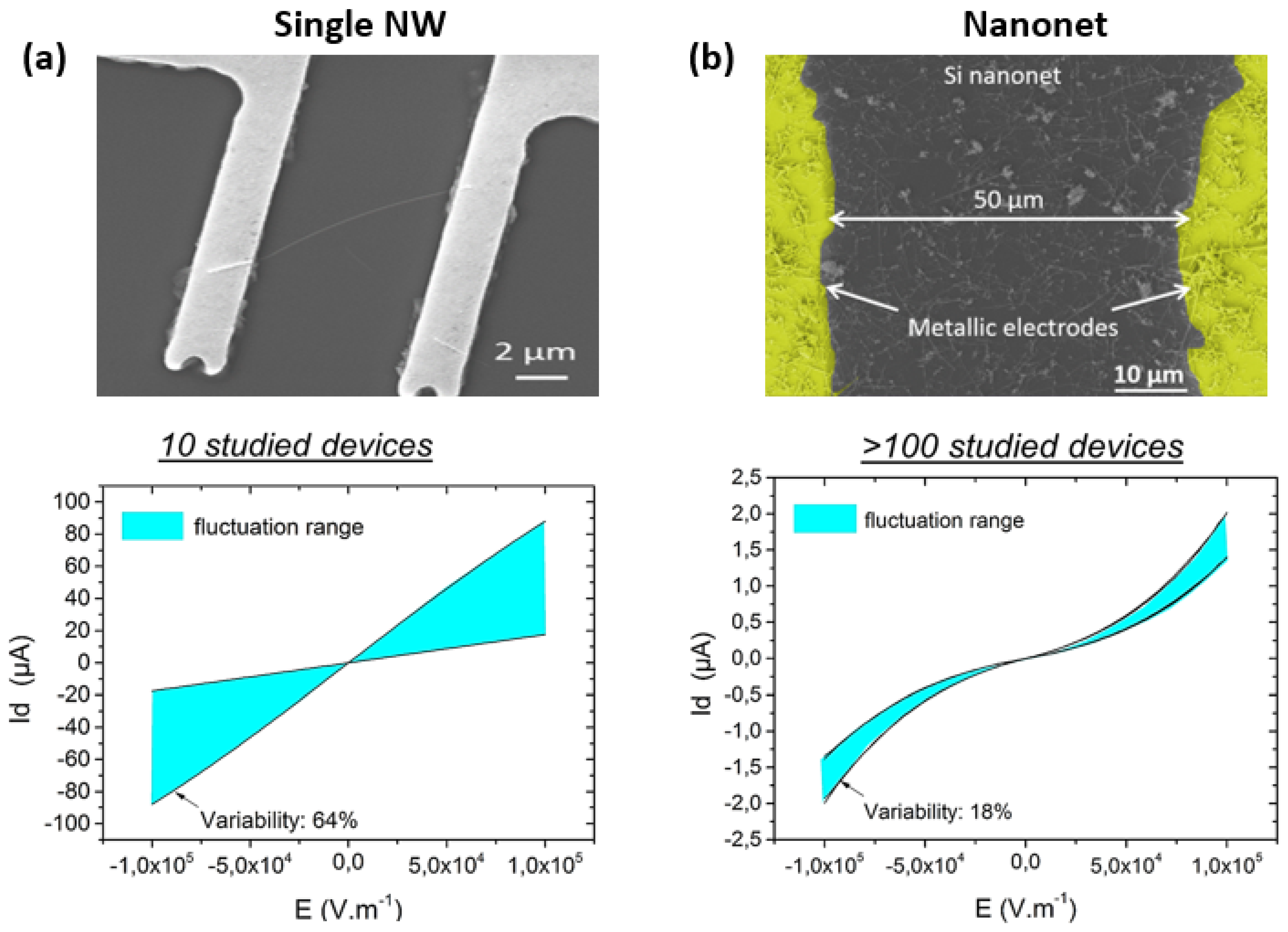
4.4. Fault Tolerance and Reproducibility
5. Silicon Nanowire Growth
5.1. Vapor Phase
5.1.1. Low Pressure
5.1.2. High Pressure
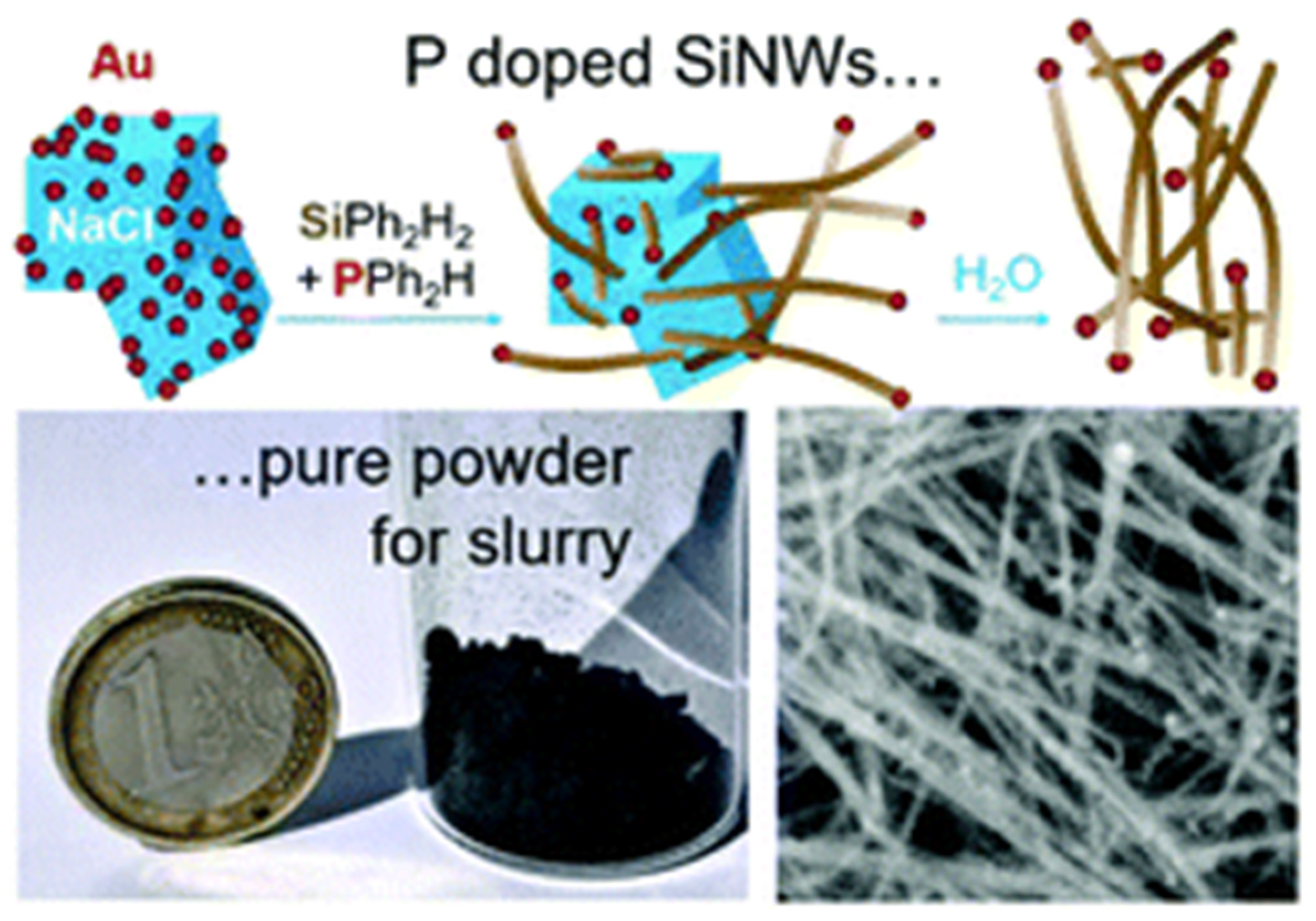
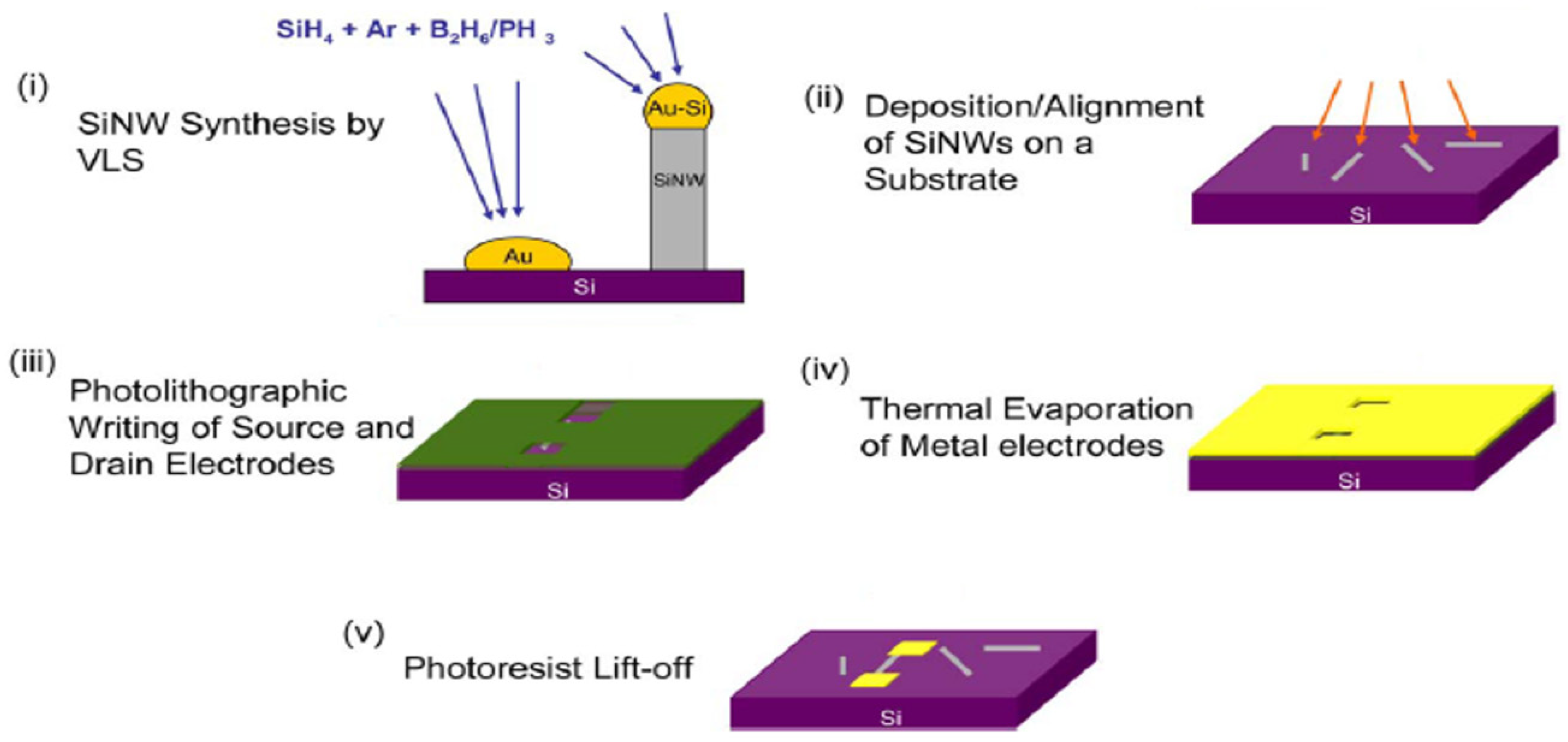
5.2. Liquid (Solution) Phase
5.3. Summary on Growth
6. SiNW Collective Handling
6.1. Network with Preferential Orientation
6.1.1. Drop-Casting
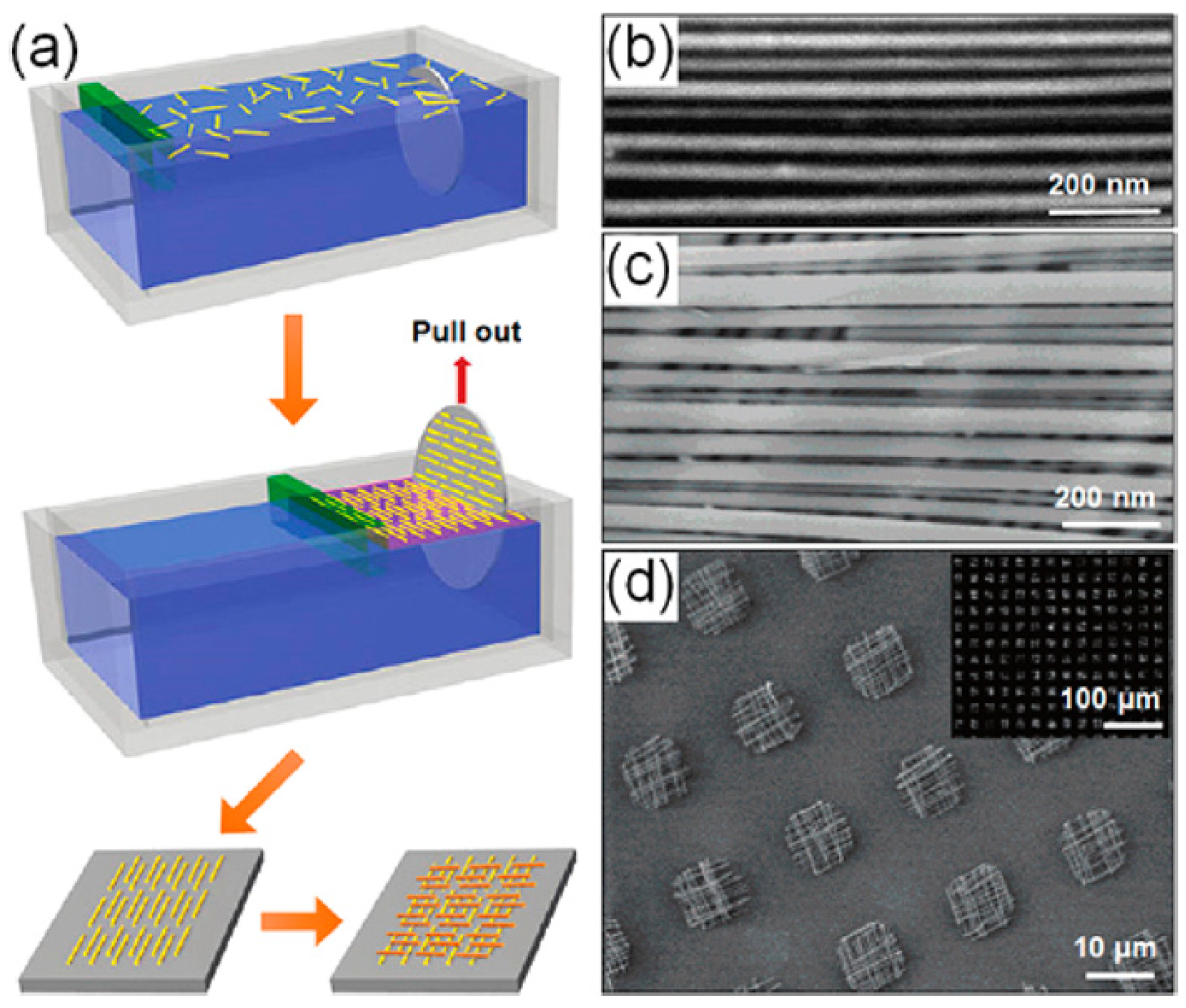
6.1.2. Fluidic Directed Assembly
6.1.3. Langmuir–Blodgett Assembly
6.1.4. Blown-Bubble Films
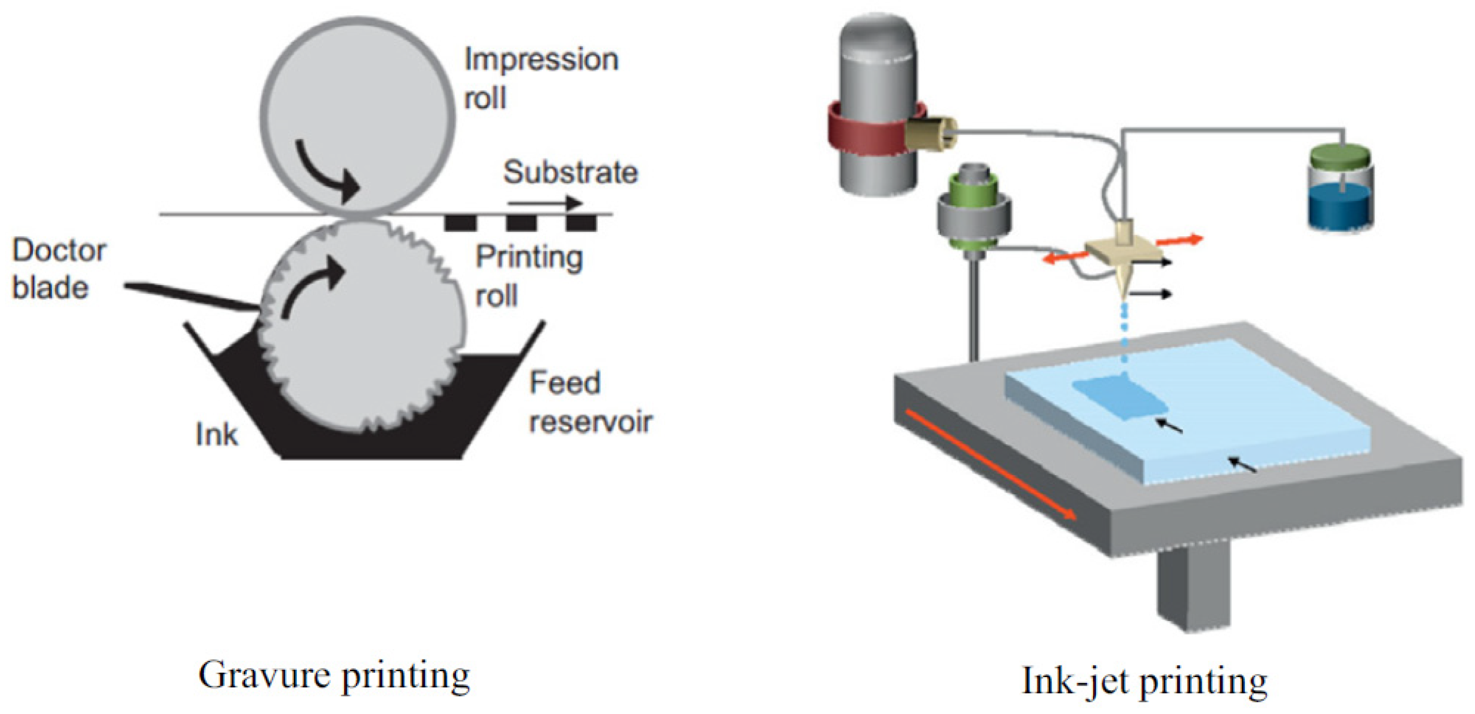
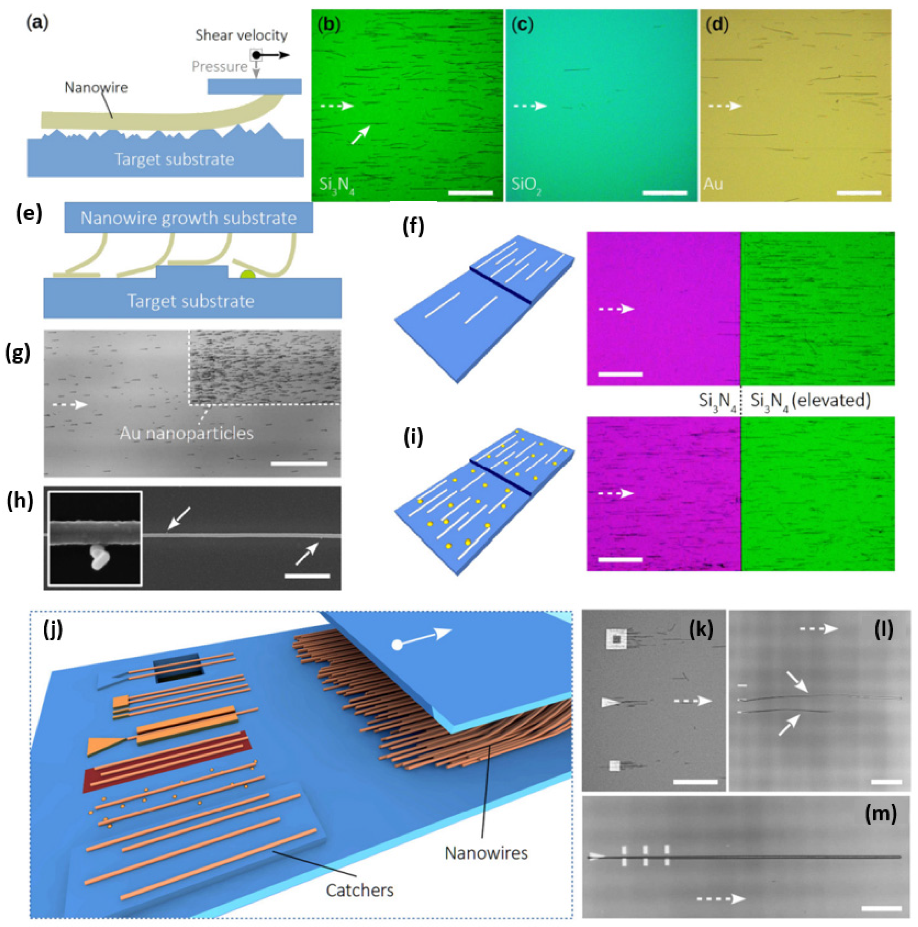
6.1.5. Contact Printing
6.2. Random Networks
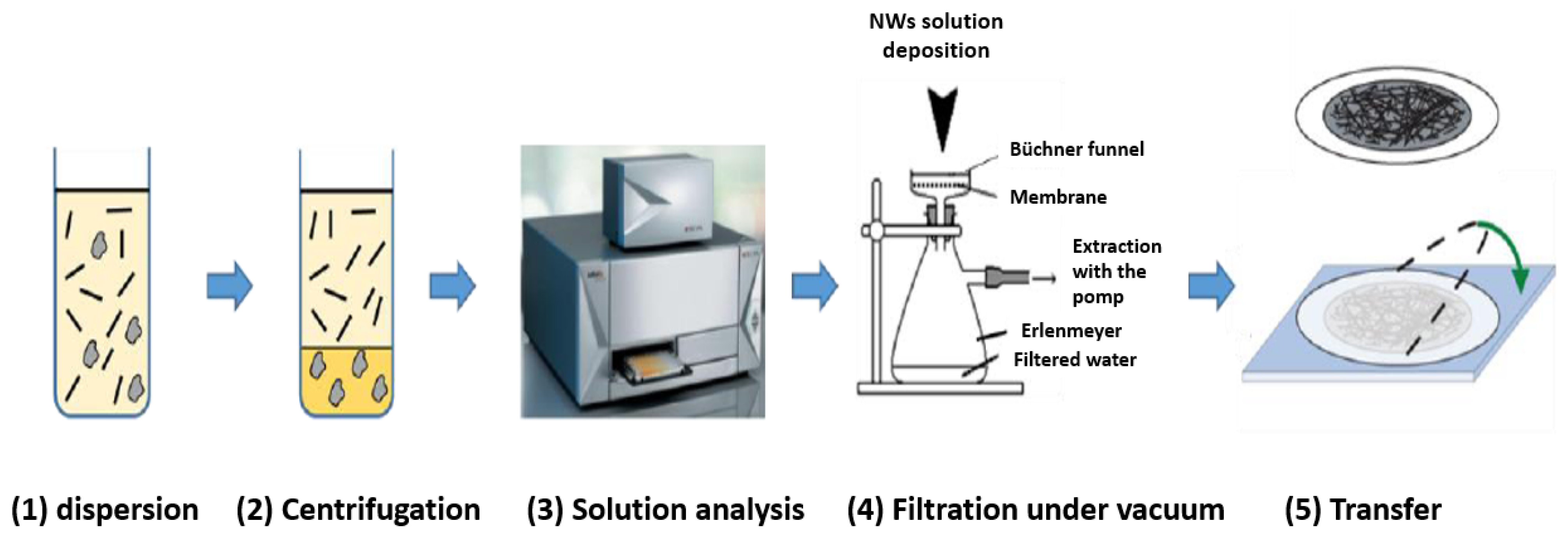
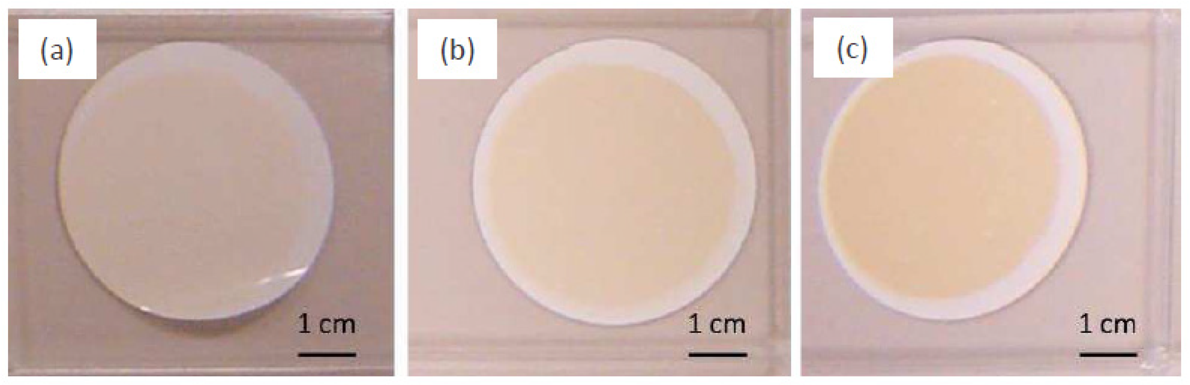
6.2.1. Vacuum Filtration
6.2.2. Spray Coating
6.3. Advantages and Disadvantages of Each Technique
7. Silicon Nanowire-Based Transistors
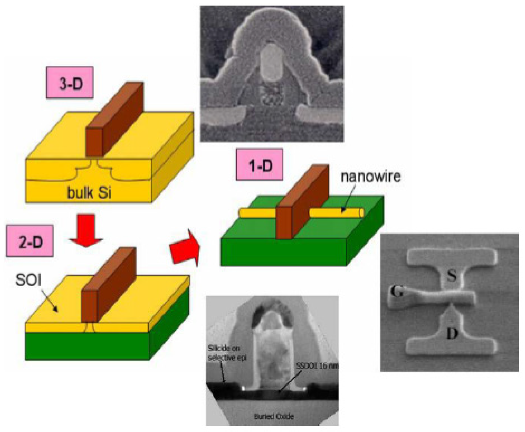
7.1. Integration Process
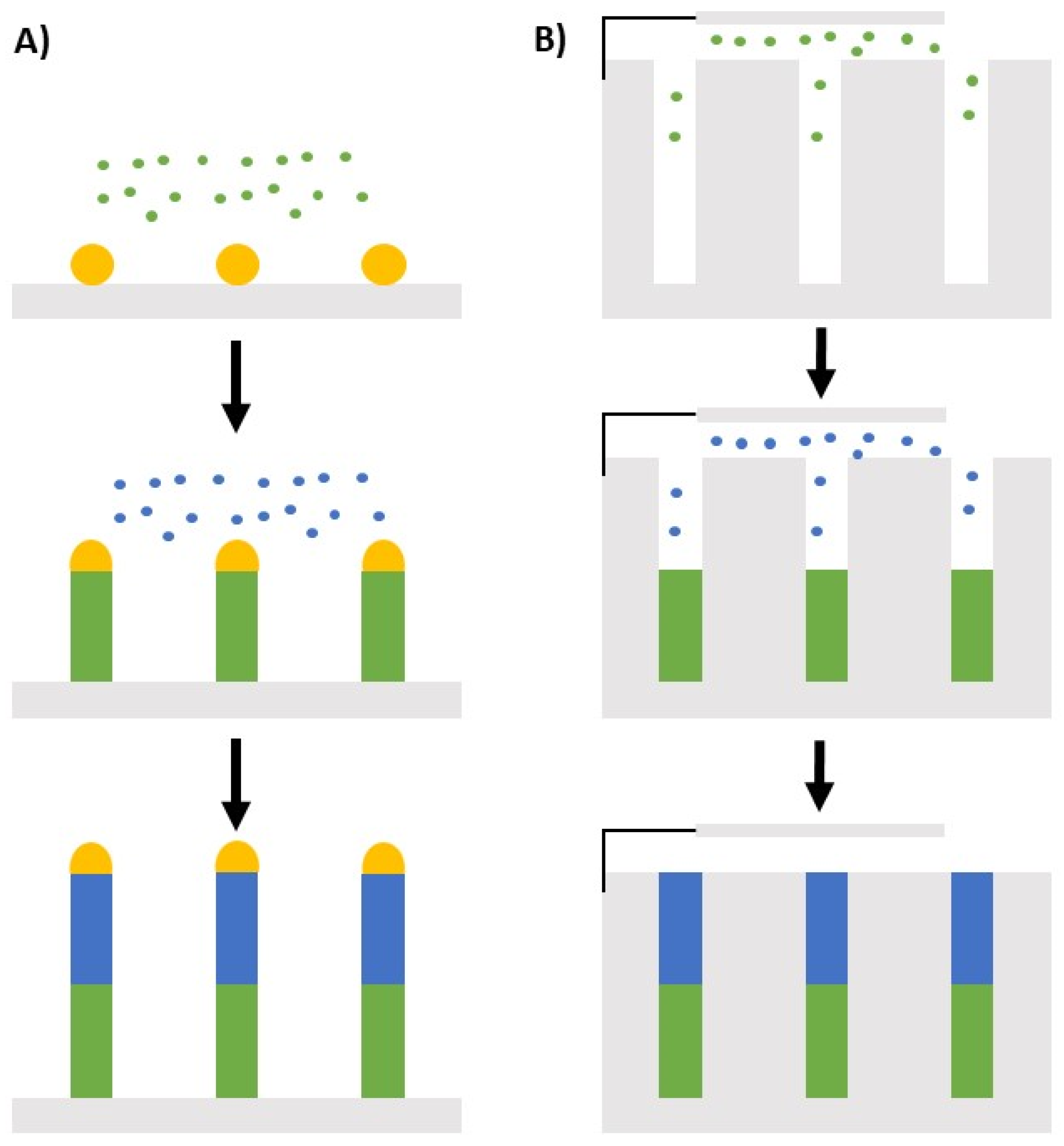
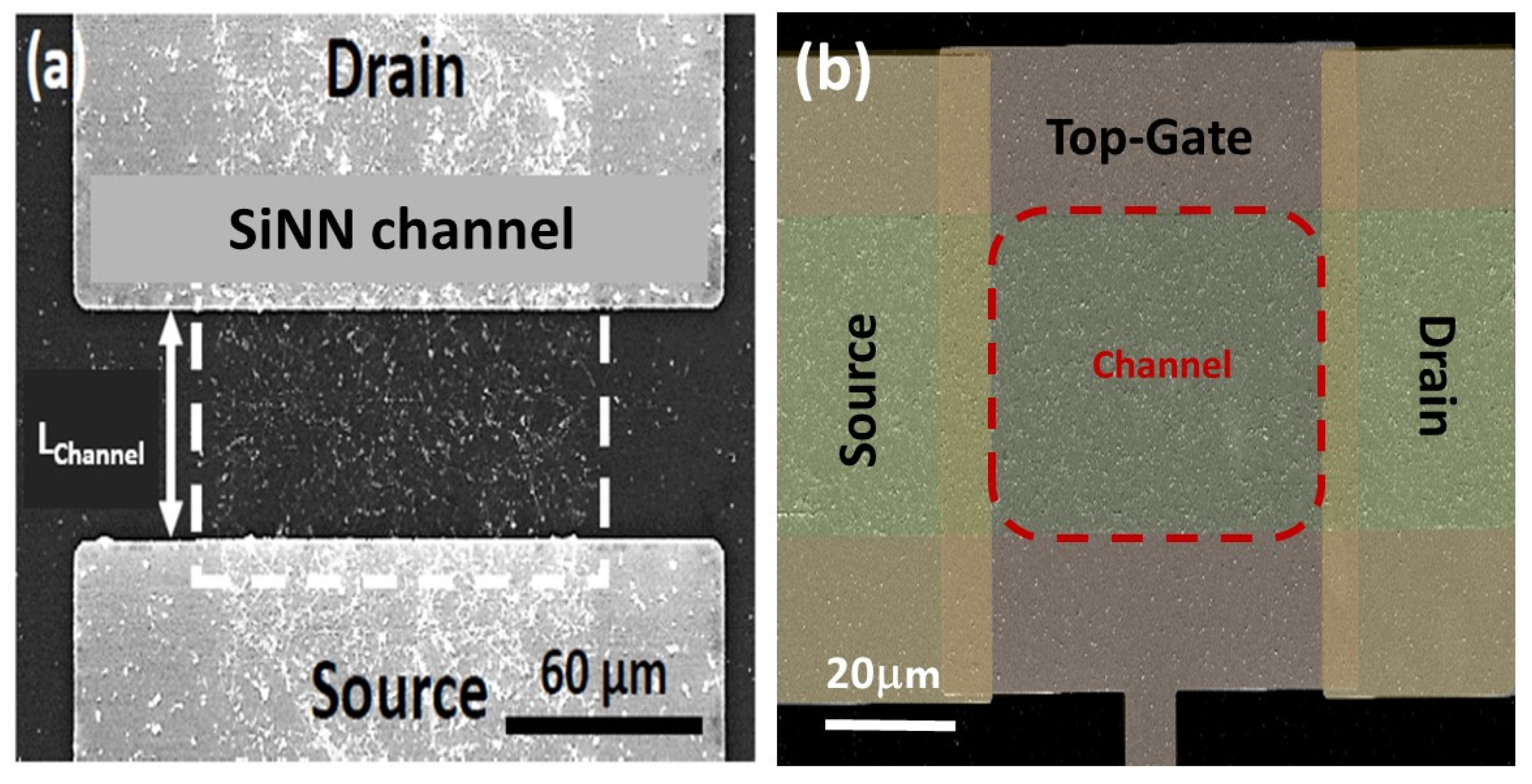
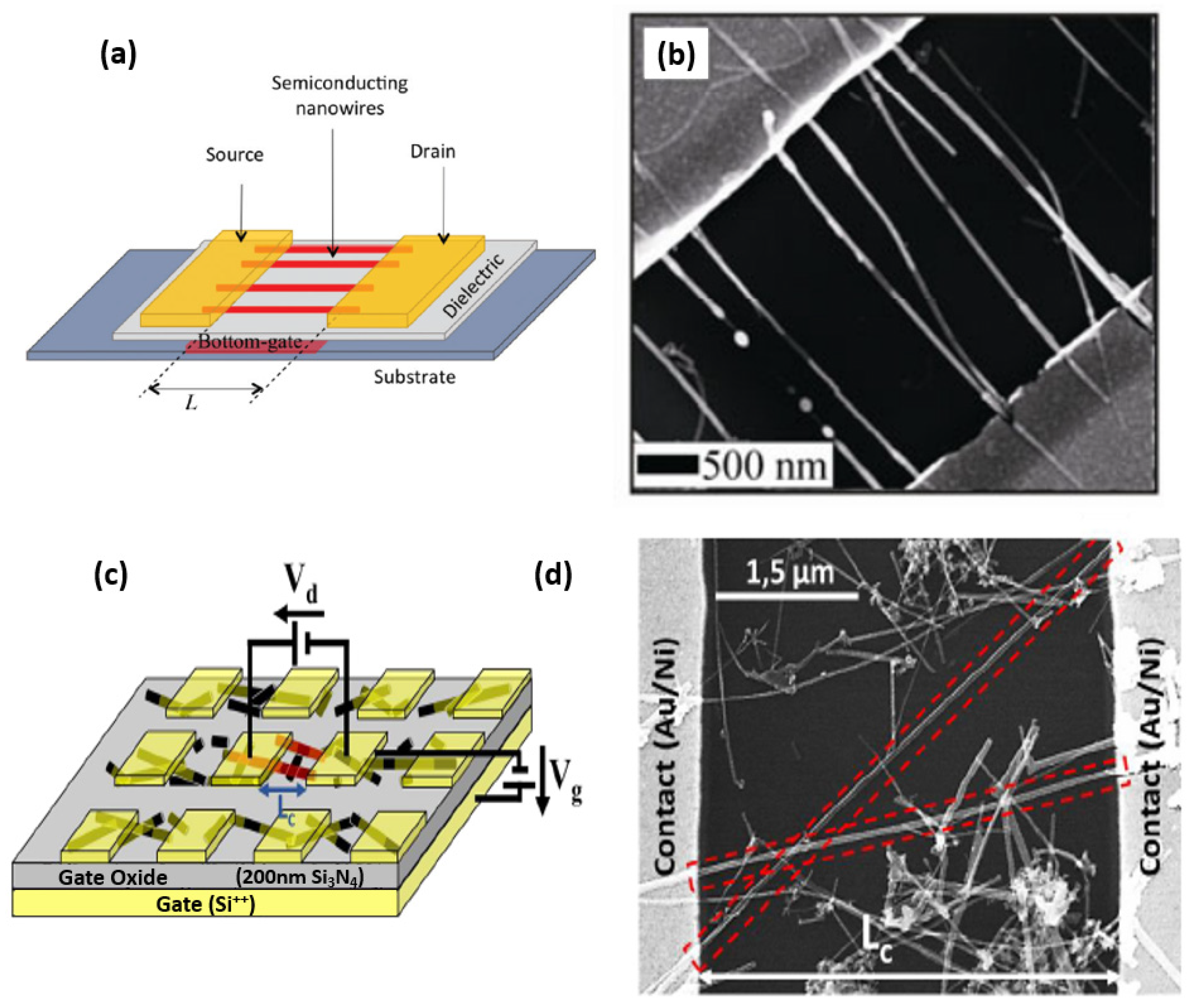
7.1.1. Single Nanowire FETs (Single-SiNW-FETs)
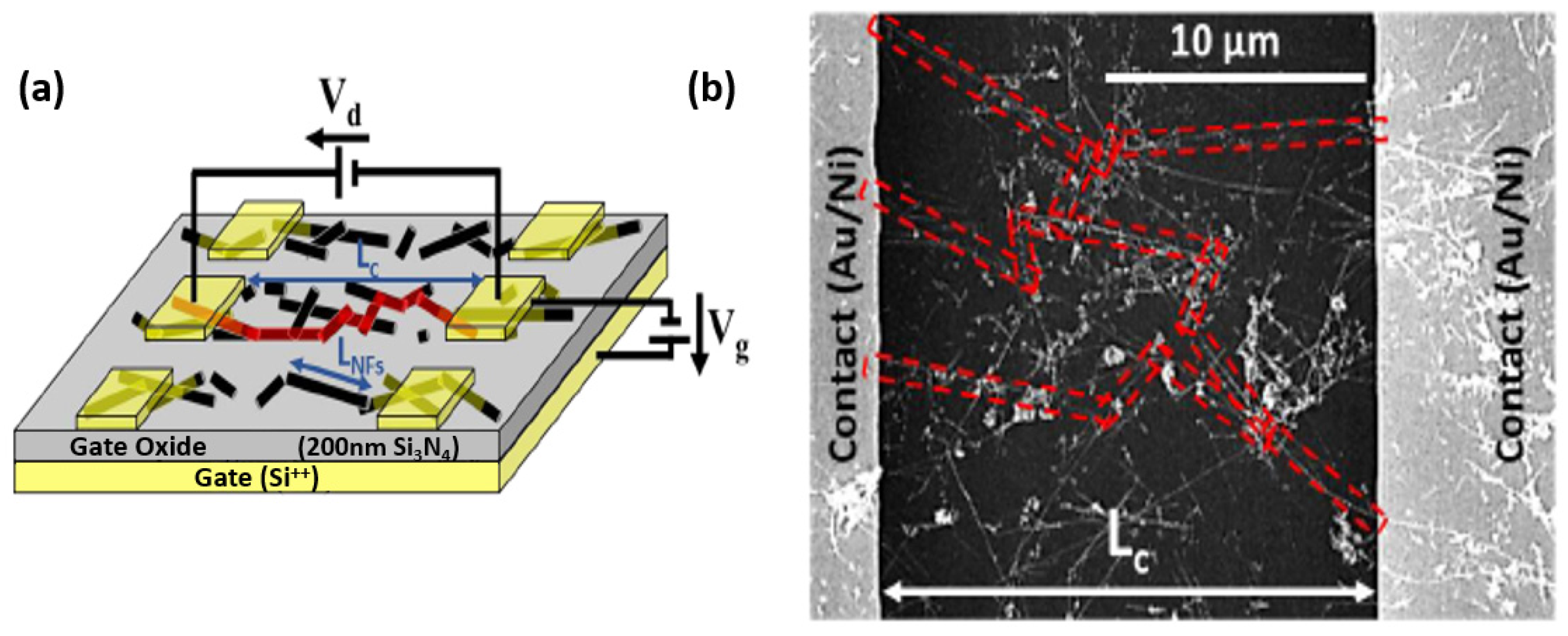
7.1.2. Silicon Nanonet FETs (SiNN-FETs)
- -
- Sintering of the NW–NW junctions and passivation of the NN to stabilize electrical properties (see Section 8.1 Sintering and Section 8.2 Surface and Interface).
- -
- NN patterning to define the channel geometry (Figure 23i-0–i-5).
- -
- Deposition of the source/drain contacts (Figure 23ii-0–ii-5).
- -
- Silicidation of the source/drain contacts (see Section 8.3 Silicidation).
7.1.3. Multiple-Parallel-Channel FETs (MPC-FETs)
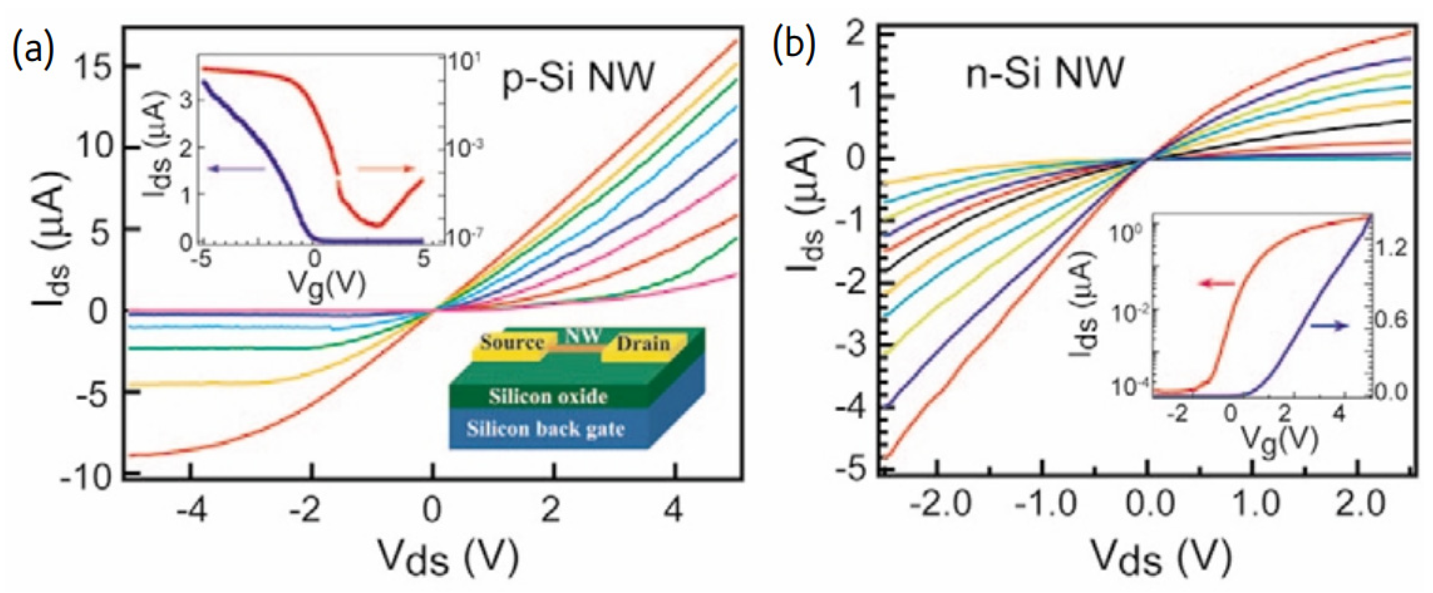
7.2. Electrical Characteristics of Single SiNW-, SiMPC-, and SiNN-FETs
8. Technological Key Elements for SiNW-Based Device Integration
8.1. Sintering
8.2. Surface and Interfaces
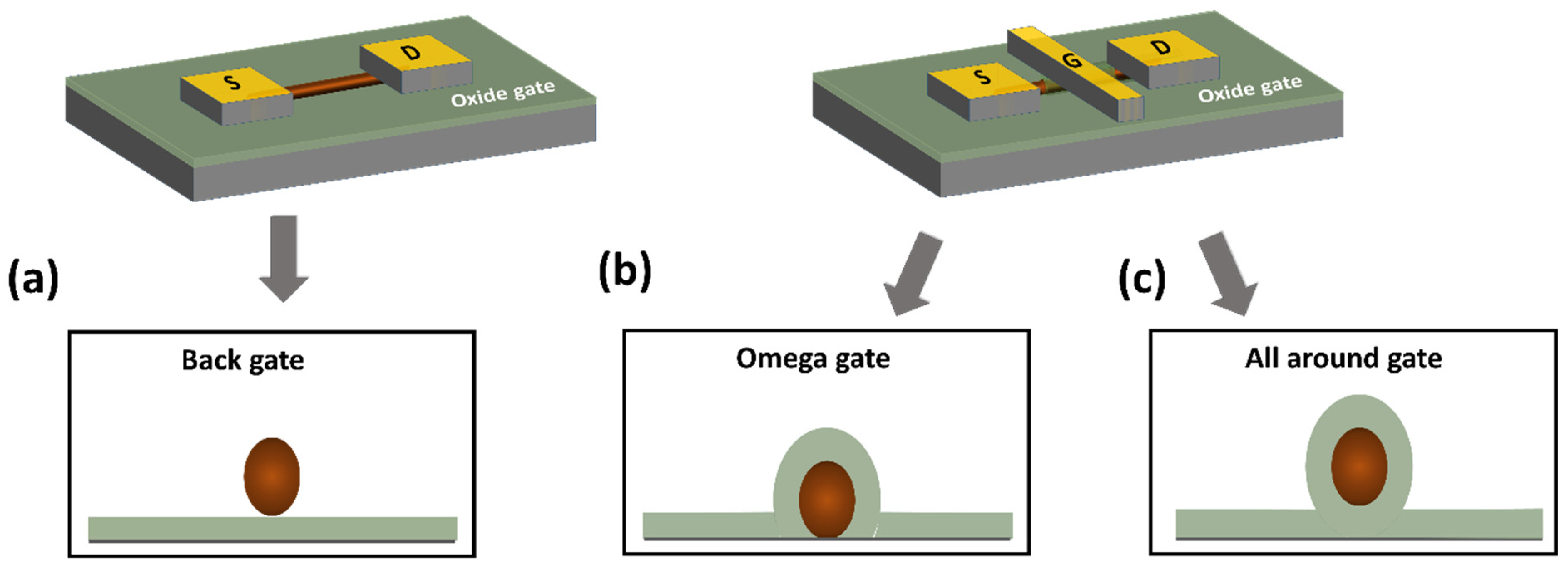
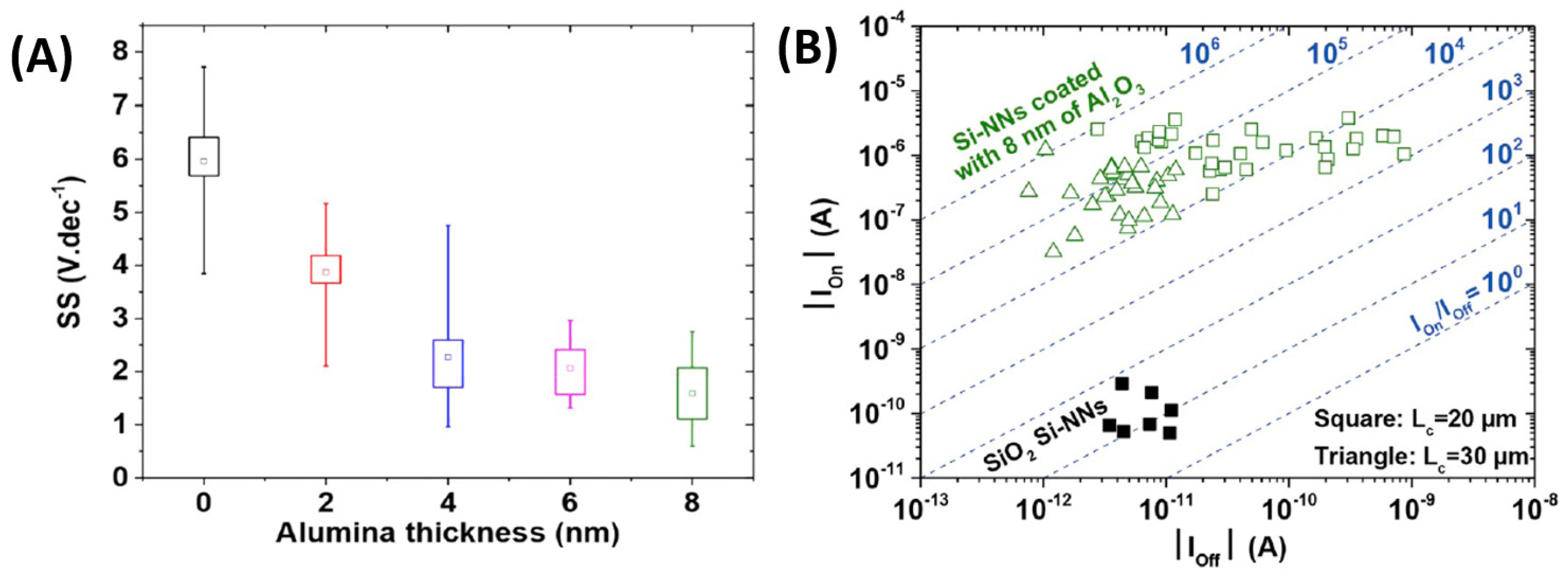
8.2.1. Modulation Thanks to Interface Surrounding the Channel
8.2.2. Modulation Thanks to Functionalization under the Channel
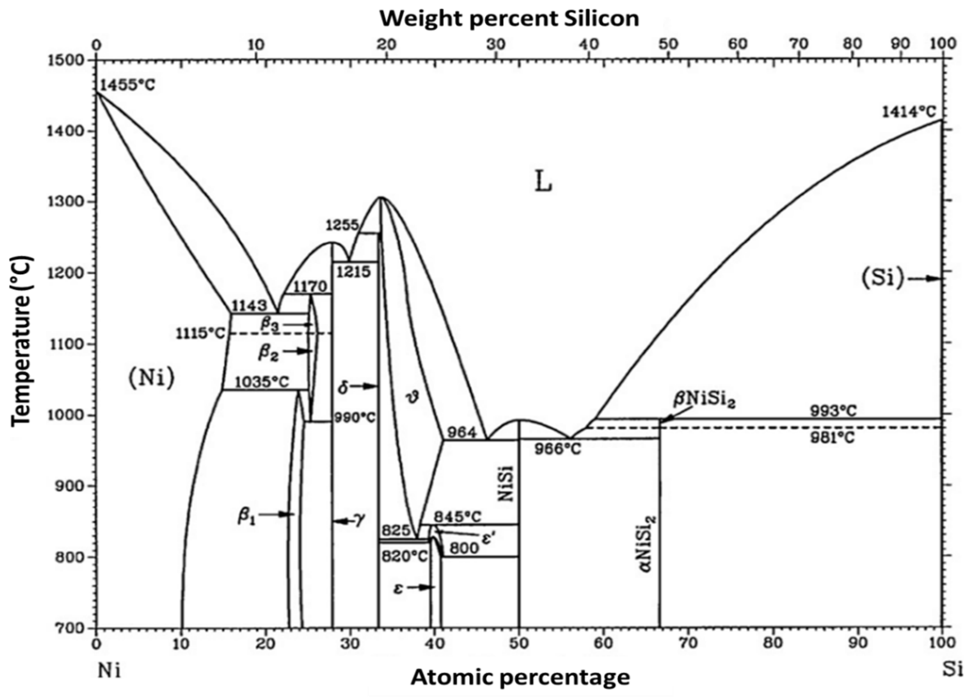
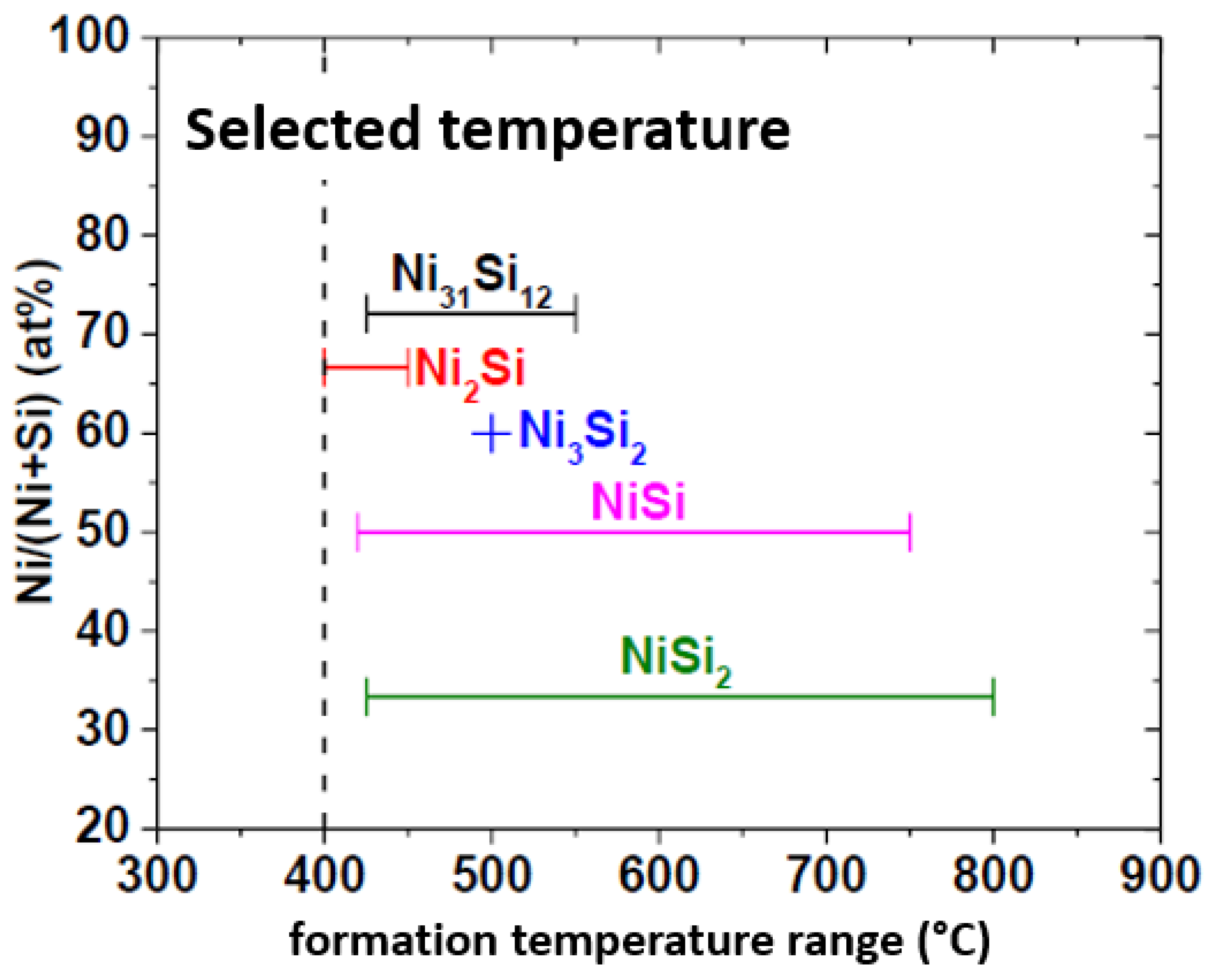
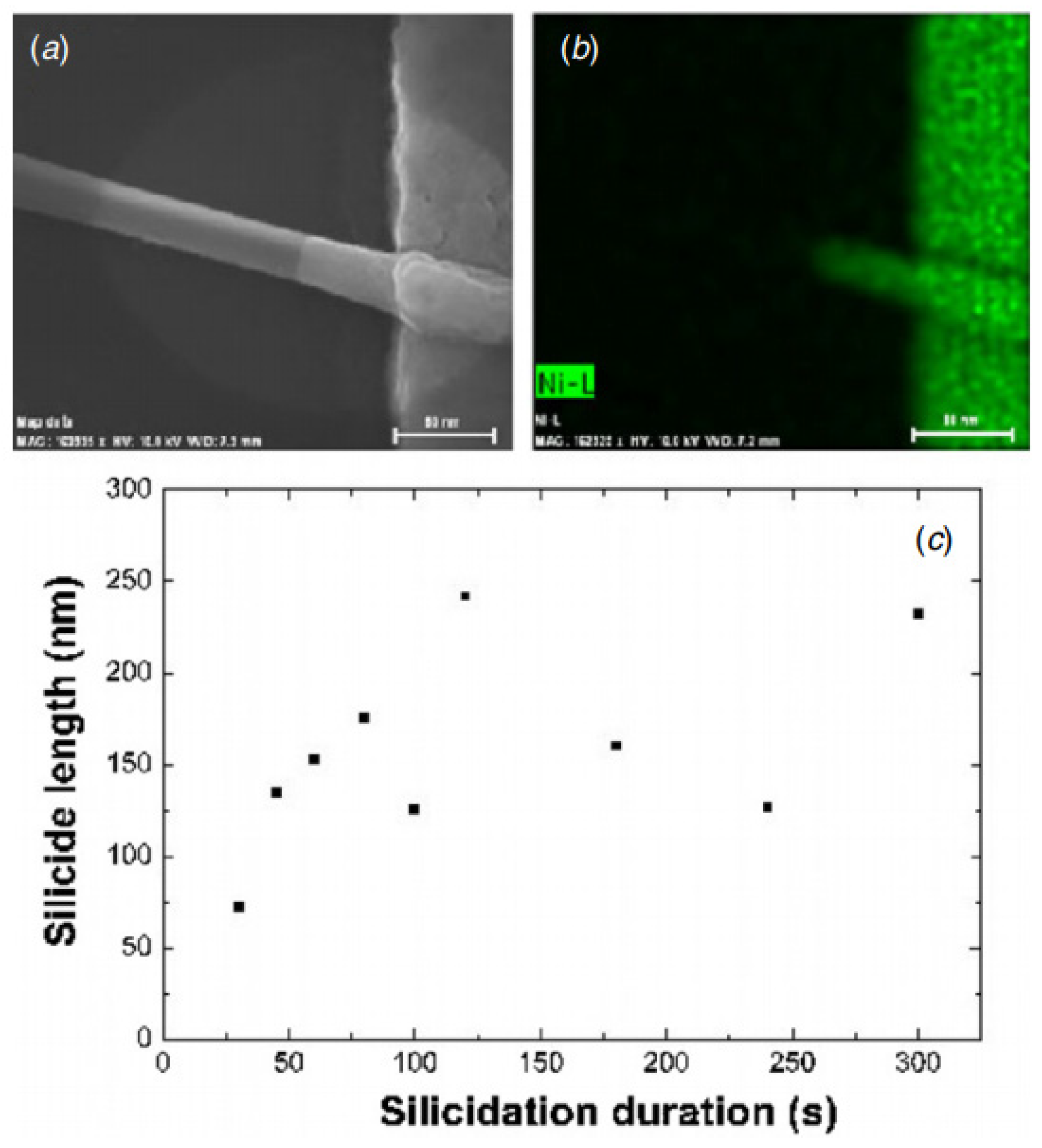
8.3. Silicidation
Silicidation of Silicon Nanowires with Nickel
9. Applications
9.1. Photodetectors
9.2. Memories
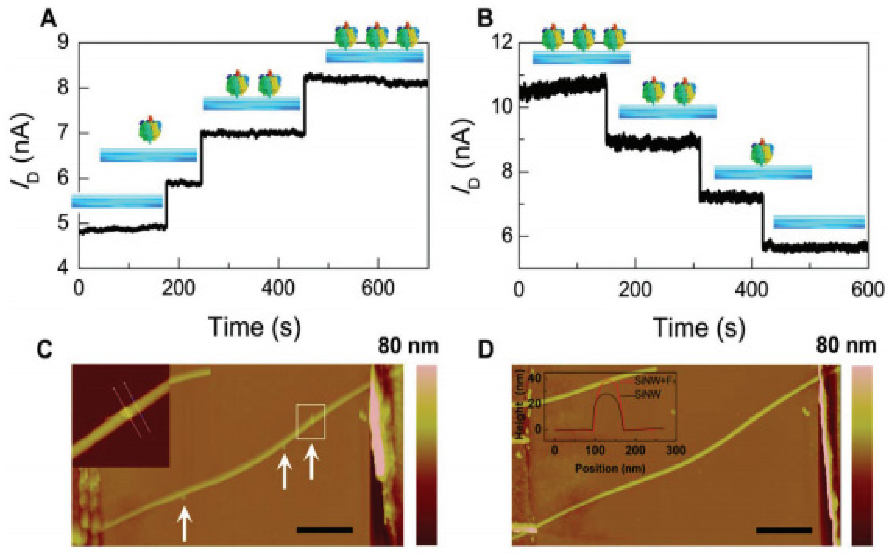
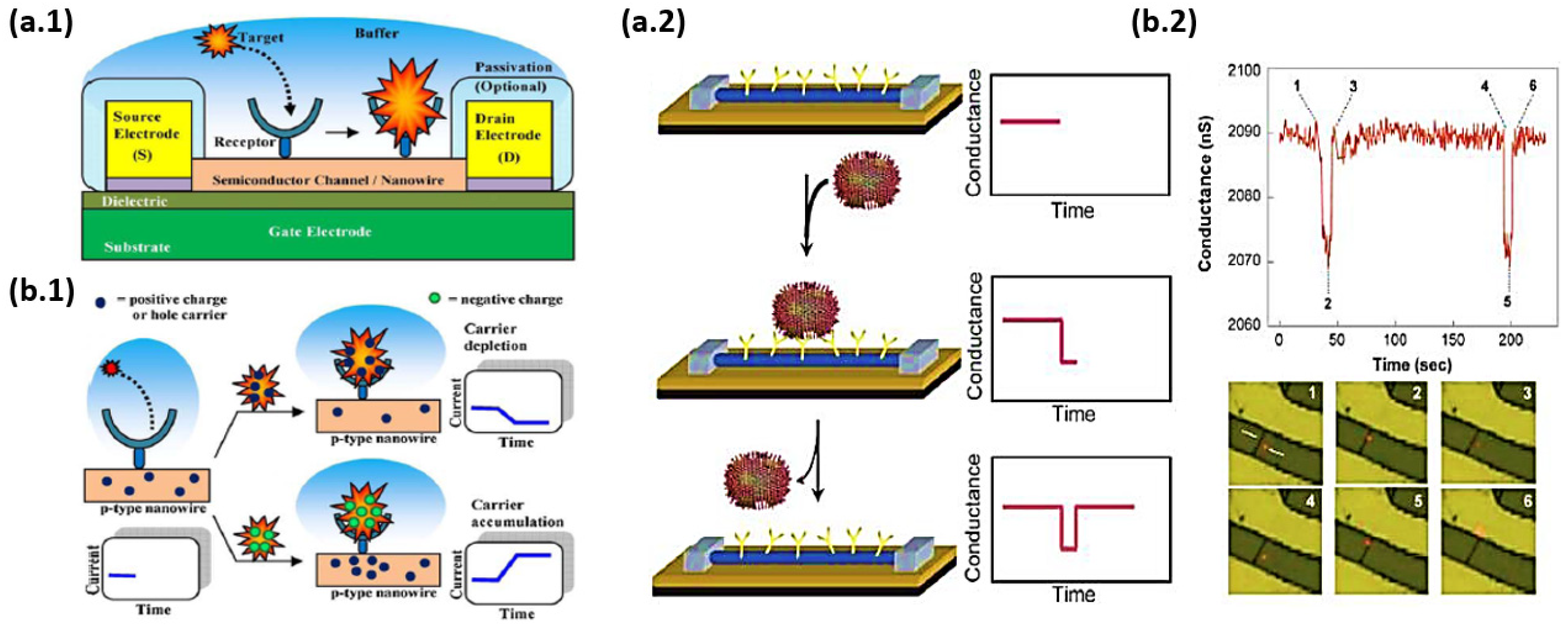
9.3. Biosensors
9.4. Gas Sensor
9.5. Thermoelectric Application
10. Conclusions
Funding
Conflicts of Interest
References
- Ramgir, N.S.; Yang, Y.; Zacharias, M. Nanowire-Based Sensors. Small 2010, 6, 1705–1722. [Google Scholar] [CrossRef] [PubMed]
- Wu, B.; Heidelberg, A.; Boland, J. Mechanical properties of ultrahigh-strength gold nanowires. Nat. Mater. 2005, 4, 525–529. [Google Scholar] [CrossRef] [PubMed]
- Rosaz, G. Intégration 3D de Nanofils Si et SiGe Pour la Réalisation de Transistors Verticaux à Canal. 2012. Available online: https://www.theses.fr/2012GRENT108 (accessed on 9 February 2022).
- Lu, W.; Xiang, J. Semiconductor Nanowires: From Next-Generation Electronics to Sustainable Energy. R. Soc. Chem. 2015, 39. Available online: http://stacks.iop.org/0022-3727/39/i=21/a=R01 (accessed on 8 February 2022).
- Liu, L.-C.; Huang, M.-J.; Yang, R.; Jeng, M.-S.; Yang, C.-C. Curvature effect on the phonon thermal conductivity of dielectric nanowires. J. Appl. Phys. 2009, 105, 104313. [Google Scholar] [CrossRef]
- Yu, B.; Meyyappan, M. Nanotechnology: Role in emerging nanoelectronics. Solid-State Electron. 2006, 50, 536–544. [Google Scholar] [CrossRef]
- How Nanowires Work. 2014, pp. 1–5. Available online: https://science.howstuffworks.com/nanowire.htm (accessed on 11 January 2022).
- Ternon, C.; Dupas, F.; Stein, S.; Aguirre, C.; Dhalluin, F.; Baron, T. Carbon Nanotube Sheet as Top Contact Electrode for Nanowires: Highly Versatile and Simple Process. J. Nanosci. Nanotechnol. 2015, 15, 1669–1673. [Google Scholar] [CrossRef] [PubMed]
- Rosaz, G.; Salem, B.; Pauc, N.; Potié, A.; Gentile, P.; Baron, T. Vertically integrated silicon-germanium nanowire field-effect transistor. Appl. Phys. Lett. 2011, 99, 193107. [Google Scholar] [CrossRef]
- Arjmand, T.; Legallais, M.; Haffner, T.; Bawedin, M.; Ternon, C.; Salem, B. Development of a robust fabrication process for single silicon nanowire-based omega gate transistors on polyamide substrate. Semicond. Sci. Technol. 2020, 36, 025003. [Google Scholar] [CrossRef]
- Rosaz, G.; Salem, B.; Pauc, N.; Gentile, P.; Potié, A.; Solanki, A.; Baron, T. High-performance silicon nanowire field-effect transistor with silicided contacts. Semicond. Sci. Technol. 2011, 26, 085020. [Google Scholar] [CrossRef]
- Morales, A.M.; Lieber, C.M. A Laser Ablation Method for the Synthesis of Crystalline Semiconductor Nanowires. Science 1998, 279, 208–211. [Google Scholar] [CrossRef]
- Yu, P.; Wu, J.; Liu, S.; Xiong, J.; Jagadish, C.; Wang, Z.M. Design and fabrication of silicon nanowires towards efficient solar cells. Nano Today 2016, 11, 704–737. [Google Scholar] [CrossRef]
- Chen, L.; Lu, W.; Lieber, C.M. Chapter 1. Semiconductor Nanowire Growth and Integration. In Semiconductor Nanowires: From Next-Generation Electronics to Sustainable Energy; Royal Society of Chemistry: London, UK, 2014; pp. 1–53. [Google Scholar] [CrossRef] [Green Version]
- Appenzeller, J.; Member, S.; Knoch, J.; Björk, M.T.; Riel, H.; Schmid, H.; Riess, W. Toward nanowire electronics. IEEE Trans. Electron Devices 2008, 55, 2827–2845. [Google Scholar] [CrossRef] [Green Version]
- Björk, M.T.; Schmid, H.; Knoch, J.; Riel, H.; Riess, W. Donor deactivation in silicon nanostructures. Nat. Nanotechnol. 2009, 4, 103–107. [Google Scholar] [CrossRef] [PubMed]
- Patolsky, F.; Lieber, C.M. Nanowire nanosensors. Mater. Today 2005, 8, 20–28. [Google Scholar] [CrossRef]
- Sohn, Y.-S.; Park, J.; Yoon, G.; Song, J.; Jee, S.-W.; Lee, J.-H.; Na, S.; Kwon, T.; Eom, K. Mechanical Properties of Silicon Nanowires. Nanoscale Res. Lett. 2009, 5, 211–216. [Google Scholar] [CrossRef] [PubMed] [Green Version]
- Dasgupta, N.P.; Sun, J.; Liu, C.; Brittman, S.; Andrews, S.C.; Lim, J.; Gao, H.; Yan, R.; Yang, P. 25th Anniversary Article: Semiconductor Nanowires—Synthesis, Characterization, and Applications. Adv. Mater. 2014, 26, 2137–2184. [Google Scholar] [CrossRef]
- Schmidt, V.; Wittemann, J.V.; Senz, S.; Gösele, U. Silicon Nanowires: A Review on Aspects of their Growth and their Electrical Properties. Adv. Mater. 2009, 21, 2681–2702. [Google Scholar] [CrossRef]
- Cui, Y.; Wei, Q.; Park, H.; Lieber, C.M. Nanowire Nanosensors for Highly Sensitive and Selective Detection of Biological and Chemical Species. Science 2001, 293, 1289–1292. [Google Scholar] [CrossRef]
- Shao, M.; Ma, D.D.D.; Lee, S. Silicon Nanowires—Synthesis, Properties, and Applications. Eur. J. Inorg. Chem. 2010, 2010, 4264–4278. [Google Scholar] [CrossRef]
- Dhahi, T.S.; Bin Hashim UD, A.; Ahmed, N.M.; Mat Taib, A. A review on the electrochemical sensors and biosensors composed of nanogaps as sensing material. J. Optoelectron. Adv. Mater. 2010, 12, 1857–1862. [Google Scholar]
- Sun, C.; Mathews, N.; Zheng, M.; Sow, C.H.; Wong, L.H.; Mhaisalkar, S.G. Aligned Tin Oxide Nanonets for High-Performance Transistors. J. Phys. Chem. C 2009, 114, 1331–1336. [Google Scholar] [CrossRef]
- Morisot, F.; Nguyen, V.H.; Montemont, C.; Maindron, T.; Munoz-Rojas, D.; Mouis, M.; Langlet, M.; Ternon, C. Al2O3, Al doped ZnO and SnO2 encapsulation of randomly oriented ZnO nanowire networks for high performance and stable electrical devices. Nanotechnology 2019, 30, 385202. [Google Scholar] [CrossRef] [PubMed]
- Langley, D.; Giusti, G.; Mayousse, C.; Celle, C.; Bellet, D.; Simonato, J.-P. Flexible transparent conductive materials based on silver nanowire networks: A review. Nanotechnology 2013, 24, 452001. [Google Scholar] [CrossRef] [PubMed]
- Legallais, M. Conception, Etude et Modélisation d’une Nouvelle Génération de Transistors à Nanofils de Silicium Pour Applications Biocapteurs. Ph.D. Dissertation, Université Grenoble Alpes, Grenoble, France, 2017. [Google Scholar]
- Pauline, S. Etude des Propriétés Structurales et électriques de Réseaux Aléatoires de Nanofils de Silicium. 2014. Available online: https://tel.archives-ouvertes.fr/tel-01162345/ (accessed on 9 February 2022).
- De, S.; Coleman, J.N. The effects of percolation in nanostructured transparent conductors. Mrs Bull. 2011, 36, 774–781. [Google Scholar] [CrossRef] [Green Version]
- Acharya, S.; Panda, A.B.; Belman, N.; Efrima, S.; Golan, Y. A Semiconductor-Nanowire Assembly of Ultrahigh Junction Density by the Langmuir–Blodgett Technique. Adv. Mater. 2006, 18, 210–213. [Google Scholar] [CrossRef]
- Li, Y.; Qian, F.; Xiang, J.; Lieber, C.M. Nanowire electronic and optoelectronic devices. Mater. Today 2006, 9, 18–27. [Google Scholar] [CrossRef]
- Kharisov, B.I.; Kharissova, O.V.; García, B.O.; Méndez, Y.P.; de la Fuente, I.G. State of the art of nanoforest structures and their applications. RSC Adv. 2015, 5, 105507–105523. [Google Scholar] [CrossRef]
- Zhong, Z.; Wang, D.; Cui, Y.; Bockrath, M.W.; Lieber, C.M. Nanowire Crossbar Arrays as Address Decoders for Integrated Nanosystems. Science 2003, 302, 1377–1379. [Google Scholar] [CrossRef] [Green Version]
- Mongillo, M.; Spathis, P.; Katsaros, G.; Gentile, P.; De Franceschi, S. Multifunctional Devices and Logic Gates with Undoped Silicon Nanowires. Nano Lett. 2012, 12, 3074–3079. [Google Scholar] [CrossRef] [Green Version]
- Gruner, G. Carbon nanonets spark new electronics. Sci. Am. 2007, 296, 76–83. [Google Scholar] [CrossRef]
- Gruner, G. Carbon nanotube films for transparent and plastic electronics. J. Mater. Chem. 2006, 16, 3533–3539. [Google Scholar] [CrossRef]
- Hammersley, J.M. Percolation processes. Math. Proc. Camb. Philos. Soc. 1957, 53, 642–645. [Google Scholar] [CrossRef]
- Kirkpatrick, S. Percolation and Conduction. Rev. Mod. Phys. 1973, 45, 574–588. [Google Scholar] [CrossRef]
- Serre, P.; Mongillo, M.; Periwal, P.; Baron, T.; Ternon, C. Percolating silicon nanowire networks with highly reproducible electrical properties. Nanotechnology 2014, 26, 15201. [Google Scholar] [CrossRef]
- Hill, D.J.; Teitsworth, T.S.; Ritchie, E.T.; Atkin, J.M.; Cahoon, J.F. Interplay of Surface Recombination and Diode Geometry for the Performance of Axial p–i–n Nanowire Solar Cells. ACS Nano 2018, 12, 10554–10563. [Google Scholar] [CrossRef]
- Sze, S.; Irvin, J. Resistivity, mobility and impurity levels in GaAs, Ge, and Si at 300° K. Solid-State Electron. 1968, 11, 599–602. [Google Scholar] [CrossRef]
- Heo, K.; Cho, E.; Yang, J.-E.; Kim, M.-H.; Lee, M.; Lee, B.Y.; Kwon, S.G.; Lee, M.-S.; Jo, M.-H.; Choi, H.-J.; et al. Large-Scale Assembly of Silicon Nanowire Network-Based Devices Using Conventional Microfabrication Facilities. Nano Lett. 2008, 8, 4523–4527. [Google Scholar] [CrossRef]
- Whang, D.; Jin, S.; Wu, Y.; Lieber, C.M. Large-Scale Hierarchical Organization of Nanowire Arrays for Integrated Nanosystems. Nano Lett. 2003, 3, 1255–1259. [Google Scholar] [CrossRef]
- Mulazimoglu, E.; Coskun, S.; Gunoven, M.; Butun, B.; Ozbay, E.; Turan, R.; Unalan, H. Silicon nanowire network metal-semiconductor-metal photodetectors. Appl. Phys. Lett. 2013, 103, 83114. [Google Scholar] [CrossRef]
- Rabbani, M.G.; Patil, S.R.; Verma, A.; Villarreal, J.E.; Korgel, B.A.; Nekovei, R.; Khader, M.M.; Darling, R.B.; Anantram, M.P. Zero-bias photocurrents in highly-disordered networks of Ge and Si nanowires. Nanotechnology 2015, 27, 045201. [Google Scholar] [CrossRef] [Green Version]
- Dalal, S.H.; Unalan, H.; Zhang, Y.; Hiralal, P.; Gangloff, L.; Flewitt, A.; Amaratunga, G.A.J.; Milne, W.I. Synthesis of ZnO nanowires for thin film network transistors. Carbon Nanotub. Assoc. Devices 2008, 7037, 172–178. [Google Scholar] [CrossRef]
- Legallais, M.; Nguyen, T.T.T.; Cazimajou, T.; Mouis, M.; Salem, B.; Ternon, C. Material engineering of percolating silicon nanowire networks for reliable and efficient electronic devices. Mater. Chem. Phys. 2019, 238, 121871. [Google Scholar] [CrossRef]
- Ternon, C.; Serre, P.; Lebrun, J.-M.; Brouzet, V.; Legallais, M.; David, S.; Luciani, T.; Pascal, C.; Baron, T.; Missiaen, J.-M. Low Temperature Processing to Form Oxidation Insensitive Electrical Contact at Silicon Nanowire/Nanowire Junctions. Adv. Electron. Mater. 2015, 1, 1500172. [Google Scholar] [CrossRef]
- Shu, L.; Liang, R.; Rao, Z.; Fei, L.; Ke, S.; Wang, Y. Flexoelectric materials and their related applications: A focused review. J. Adv. Ceram. 2019, 8, 153–173. [Google Scholar] [CrossRef] [Green Version]
- Liang, X.; Hu, S.; Shen, S. Effects of surface and flexoelectricity on a piezoelectric nanobeam. Smart Mater. Struct. 2014, 23, 035020. [Google Scholar] [CrossRef]
- Wu, X.; Kulkarni, J.S.; Collins, G.; Petkov, N.; Almécija, D.; Boland, J.J.; Erts, D.; Holmes, J.D. Synthesis and Electrical and Mechanical Properties of Silicon and Germanium Nanowires. Chem. Mater. 2008, 20, 5954–5967. [Google Scholar] [CrossRef]
- Feng, G.; Nix, W.D.; Yoon, Y.; Lee, C.J. A study of the mechanical properties of nanowires using nanoindentation. J. Appl. Phys. 2006, 99, 74304. [Google Scholar] [CrossRef]
- Lee, B.; Rudd, R.E. First-principles calculation of mechanical properties of Si⟨001⟩ nanowires and comparison to nanomechanical theory. Phys. Rev. B 2007, 75, 195328. [Google Scholar] [CrossRef] [Green Version]
- Park, S.; Kim, J.; Park, J.; Lee, J.; Choi, Y.; Kwon, O. Molecular dynamics study on size-dependent elastic properties of silicon nanocantilevers. Thin Solid Films 2005, 492, 285–289. [Google Scholar] [CrossRef]
- Zhu, Y.; Xu, F.; Qin, Q.; Fung, W.Y.; Lu, W. Mechanical Properties of Vapor−Liquid−Solid Synthesized Silicon Nanowires. Nano Lett. 2009, 9, 3934–3939. [Google Scholar] [CrossRef] [Green Version]
- Sadeghian, H.; Yang, C.-K.; Gavan, K.B.; Goosen, J.; Van Der Drift, E.W.J.M.; Van Der Zant, H.S.J.; Bossche, A.; French, P.J.; Van Keulen, F. Some considerations of effects-induced errors in resonant cantilevers with the laser deflection method. J. Micromech. Microeng. 2010, 20, 105027. [Google Scholar] [CrossRef]
- Steighner, M.S.; Snedeker, L.P.; Boyce, B.L.; Gall, K.; Miller, D.C.; Muhlstein, C. Dependence on diameter and growth direction of apparent strain to failure of Si nanowires. J. Appl. Phys. 2011, 109, 33503. [Google Scholar] [CrossRef]
- Sadeghian, H.; Yang, C.-K.; Goosen, J.; Bossche, A.; Staufer, U.; French, P.J.; Van Keulen, F. Effects of size and defects on the elasticity of silicon nanocantilevers. J. Micromech. Microeng. 2010, 20, 064012. [Google Scholar] [CrossRef] [Green Version]
- Röhlig, C.-C.; Niebelschütz, M.; Brueckner, K.; Tonisch, K.; Ambacher, O.; Cimalla, V. Elastic properties of nanowires. Phys. Status Solidi 2010, 247, 2557–2570. [Google Scholar] [CrossRef]
- Kim, Y.-J.; Son, K.; Choi, I.-C.; Park, W.I.; Jang, J.-I. Exploring Nanomechanical Behavior of Silicon Nanowires: AFM Bending Versus Nanoindentation. Adv. Funct. Mater. 2010, 21, 279–286. [Google Scholar] [CrossRef]
- Wanekaya, A.K.; Chen, W.; Myung, N.V.; Mulchandani, A. Nanowire-Based Electrochemical Biosensors. Electroanalysis 2006, 18, 533–550. [Google Scholar] [CrossRef]
- Zhao, X.; Wei, C.-M.; Yang, L.; Chou, M.-Y. Quantum Confinement and Electronic Properties of Silicon Nanowires. Phys. Rev. Lett. 2004, 92, 236805. [Google Scholar] [CrossRef] [PubMed]
- Lu, A. Theoretical Study of Electronic and Electrical Properties of Silicon Nanowires. Public Health, 2007. Available online: http://lbms03.cityu.edu.hk/theses/c_ftt/phd-ap-b22687658f.pdf (accessed on 9 February 2022).
- Sacconi, F.; Persson, M.P.; Povolotskyi, M.; Latessa, L.; Pecchia, A.; Gagliardi, A.; Balint, A.; Fraunheim, T.; Di Carlo, A. Electronic and transport properties of silicon nanowires. J. Comput. Electron. 2007, 6, 329–333. [Google Scholar] [CrossRef]
- Saitta, A.M.; Buda, F.; Fiumara, G.; Giaquinta, P.V. Ab initiomolecular-dynamics study of electronic and optical properties of silicon quantum wires: Orientational effects. Phys. Rev. B 1996, 53, 1446–1451. [Google Scholar] [CrossRef] [Green Version]
- Matsuda, Y.; Tahir-Kheli, J.; Goddard, W.A. Surface and Electronic Properties of Hydrogen Terminated Si [001] Nanowires. J. Phys. Chem. C 2011, 115, 12586–12591. [Google Scholar] [CrossRef] [Green Version]
- Haick, H.; Hurley, P.T.; Hochbaum, A.I.; Yang, P.; Lewis, N.S. Electrical Characteristics and Chemical Stability of Non-Oxidized, Methyl-Terminated Silicon Nanowires. J. Am. Chem. Soc. 2006, 128, 8990–8991. [Google Scholar] [CrossRef] [PubMed] [Green Version]
- Yuan, G.D.; Zhou, Y.B.; Guo, C.S.; Zhang, W.J.; Tang, Y.B.; Li, Y.Q.; Chen, Z.H.; He, Z.B.; Wang, P.F.; Bello, I.; et al. Tunable Electrical Properties of Silicon Nanowires via Surface-Ambient Chemistry. ACS Nano 2010, 4, 3045–3052. [Google Scholar] [CrossRef] [PubMed]
- Zhao, J.; Buia, C.; Han, J.; Lu, J.P. Quantum transport properties of ultrathin silver nanowires. Nanotechnology 2003, 14, 501–504. [Google Scholar] [CrossRef] [Green Version]
- Wiecha, P.R.; Cuche, A.; Arbouet, A.; Girard, C.; Colas des Francs, G.; Lecestre, A.; Paillard, V. Strongly Directional Scattering from Dielectric Nanowires. ACS Photonics 2018, 4, 2036–2046. [Google Scholar] [CrossRef] [Green Version]
- Nair, P.R.; Alam, M.A. Design Considerations of Silicon Nanowire Biosensors. IEEE Trans. Electron Devices 2007, 54, 3400–3408. [Google Scholar] [CrossRef]
- Legallais, M.; Nguyen, T.T.T.; Cazimajou, T.; Mouis, M.; Arjmand, T.; Salem, B.; Ternon, C. Role played by the nanowire/nanowire junctions in the electrical properties of semiconductor percolating silicon nanowire networks. J. Appl. Phys. 2020, 128, 204501. [Google Scholar] [CrossRef]
- Basori, R.; Samanta, S. Diameter dependent threshold voltage modification of resistive state switching in organometallic single nanowire devices (diameter∼10–100 nm). Appl. Phys. Lett. 2018, 113, 123507. [Google Scholar] [CrossRef]
- Nguyen, B.M.; Taur, Y.; Picraux, S.T.; Dayeh, S.A. Diameter-independent hole mobility in Ge/Si core/shell nanowire field effect transistors. Nano Lett. 2014, 14, 585–591. [Google Scholar]
- Li, J.; He, G.; Ueno, H.; Jia, C.; Noji, H.; Qi, C.; Guo, X. Direct real-time detection of single proteins using silicon nanowire-based electrical circuits. Nanoscale 2016, 8, 16172–16176. [Google Scholar] [CrossRef]
- Feng, S.; Yu, D.; Zhang, H.; Bai, Z.; Ding, Y. The growth mechanism of silicon nanowires and their quantum confinement effect. J. Cryst. Growth 2000, 209, 513–517. [Google Scholar] [CrossRef]
- Baek, E.; Das, N.R.; Cannistraci, C.V.; Rim, T.; Bermúdez, G.S.C.; Nych, K.; Cho, H.; Kim, K.; Baek, C.-K.; Makarov, D.; et al. Intrinsic plasticity of silicon nanowire neurotransistors for dynamic memory and learning functions. Nat. Electron. 2020, 3, 398–408. [Google Scholar] [CrossRef]
- Zhang, H.; Kikuchi, N.; Ohshima, N.; Kajisa, T.; Sakata, T.; Izumi, T.; Sone, H. Design and Fabrication of Silicon Nanowire-Based Biosensors with Integration of Critical Factors: Toward Ultrasensitive Specific Detection of Biomolecules. ACS Appl. Mater. Interfaces 2020, 12, 51808–51819. [Google Scholar] [CrossRef] [PubMed]
- Ahoulou, S.; Perret, E.; Nedelec, J.-M. Functionalization and Characterization of Silicon Nanowires for Sensing Applications: A Review. Nanomaterials 2021, 11, 999. [Google Scholar] [CrossRef]
- Calistri-Yeh, M.; Kramer, E.J.; Sharma, R.; Zhao, W.; Rafailovich, M.H.; Sokolov, A.J.; Brock, J.D. Thermal Stability of Self-Assembled Monolayers from Alkylchlorosilanes. Langmuir 1996, 12, 2747–2755. [Google Scholar] [CrossRef]
- Steinbach, A.M.; Sandner, T.; Nilsen, M.; Hua, X.; Sivakumar, R.; Geiger, D.; Moeinian, A.; Strehle, S. The Electronic Properties of Silicon Nanowires during Their Dissolution under Simulated Physiological Conditions. Appl. Sci. 2019, 9, 804. [Google Scholar] [CrossRef] [Green Version]
- Bashouti, M.Y.; Sardashti, K.; Ristein, J.; Christiansen, S. Kinetic study of H-terminated silicon nanowires oxidation in very first stages. Nanoscale Res. Lett. 2013, 8, 41. [Google Scholar] [CrossRef] [Green Version]
- Liu, B.; Wang, Y.; Ho, T.-T.; Lew, K.-K.; Eichfeld, S.M.; Redwing, J.M.; Mayer, T.S.; Mohney, S.E. Oxidation of silicon nanowires for top-gated field effect transistors. J. Vac. Sci. Technol. A: Vacuum Surfaces Films 2008, 26, 370. [Google Scholar] [CrossRef]
- Ma, D.D.D.; Lee, C.S.; Au, F.C.K.; Tong, S.Y.; Lee, S.T. Small-iameter Silicon Nanowire Surfaces. Science 2003, 299, 1874–1877. [Google Scholar] [CrossRef]
- Bashouti, M.Y.; Sardashti, K.; Ristein, J.; Christiansen, S.H. Early stages of oxide growth in H-terminated silicon nanowires: Determination of kinetic behavior and activation energy. Phys. Chem. Chem. Phys. 2012, 14, 11877–11881. [Google Scholar] [CrossRef] [Green Version]
- Büttner, C.C.; Zacharias, M. Retarded oxidation of Si nanowires. Appl. Phys. Lett. 2006, 89, 263106. [Google Scholar] [CrossRef] [Green Version]
- Fazzini, P.-F.; Bonafos, C.; Claverie, A.; Hubert, A.; Ernst, T.; Respaud, M. Modeling stress retarded self-limiting oxidation of suspended silicon nanowires for the development of silicon nanowire-based nanodevices. J. Appl. Phys. 2011, 110, 033524. [Google Scholar] [CrossRef]
- Harris, C.; O’Reilly, E. Nature of the band gap of silicon and germanium nanowires. Phys. E Low-Dimens. Syst. Nanostruct. 2006, 32, 341–345. [Google Scholar] [CrossRef]
- Guichard, A.R.; Barsic, D.N.; Sharma, S.; Kamins, T.; Brongersma†, M.L. Tunable Light Emission from Quantum-Confined Excitons in TiSi2-Catalyzed Silicon Nanowires. Nano Lett. 2006, 6, 2140–2144. [Google Scholar] [CrossRef] [PubMed]
- Kumar, C. UV-VIS and Photoluminescence Spectroscopy for Nanomaterials Characterization; Springer: Berlin, Germany, 2013; pp. 1–599. [Google Scholar] [CrossRef] [Green Version]
- Sivakov, V.A.; Voigt, F.; Berger, A.; Bauer, G.; Christiansen, S.H. Roughness of silicon nanowire sidewalls and room temperature photoluminescence. Phys. Rev. B 2010, 82, 125446. [Google Scholar] [CrossRef] [Green Version]
- Gonchar, K.A.; Zubairova, A.A.; Schleusener, A.; Osminkina, L.A.; Sivakov, V. Optical Properties of Silicon Nanowires Fabricated by Environment-Friendly Chemistry. Nanoscale Res. Lett. 2016, 11, 357. [Google Scholar] [CrossRef] [Green Version]
- Osminkina, L.A.; Gonchar, K.A.; Marshov, V.S.; Bunkov, K.V.; Petrov, D.V.; Golovan, L.A.; Talkenberg, F.; Sivakov, V.A.; Timoshenko, V. Optical properties of silicon nanowire arrays formed by metal-assisted chemical etching: Evidences for light localization effect. Nanoscale Res. Lett. 2012, 7, 524. [Google Scholar] [CrossRef] [Green Version]
- Gonchar, K.A.; Golovan’, L.A.; Timoshenko, V.Y.; Sivakov, V.A.; Christiansen, S. Effects of light localization in photoluminescence and Raman scattering in silicon nanostructures. Bull. Russ. Acad. Sci. Phys. 2010, 74, 1712–1714. [Google Scholar] [CrossRef]
- Golovan, L.; Gonchar, K.; Osminkina, L.; Timoshenko, V.; Petrov, G.; Yakovlev, V. Coherent anti-Stokes Raman scattering in silicon nanowire ensembles. Laser Phys. Lett. 2011, 9, 145–150. [Google Scholar] [CrossRef] [Green Version]
- Gonchar, K.A.; Osminkina, L.A.; Sivakov, V.; Lysenko, V.; Timoshenko, V. Optical properties of nanowire structures produced by the metal-assisted chemical etching of lightly doped silicon crystal wafers. Semiconductors 2014, 48, 1613–1618. [Google Scholar] [CrossRef]
- Zabotnov, S.V.; Kholodov, M.M.; Georgobiani, V.A.; Presnov, D.E.; Golovan, L.A.; Kashkarov, P.K. Photon lifetime correlated increase of Raman scattering and third-harmonic generation in silicon nanowire arrays. Laser Phys. Lett. 2016, 13, 35902. [Google Scholar] [CrossRef]
- Li, Y.; Wang, G.; Akbari-Saatlu, M.; Procek, M.; Radamson, H.H. Si and SiGe nanowire for micro-thermoelectric generator: A review of the current state of the art. Front. Mater. 2021, 8, 611078. [Google Scholar] [CrossRef]
- Zhan, T.; Yamato, R.; Hashimoto, S.; Tomita, M.; Oba, S.; Himeda, Y.; Mesaki, K.; Takezawa, H.; Yokogawa, R.; Xu, Y.; et al. Miniaturized planar Si-nanowire micro-thermoelectric generator using exuded thermal field for power generation. Sci. Technol. Adv. Mater. 2018, 19, 443–453. [Google Scholar] [CrossRef] [PubMed] [Green Version]
- Pennelli, G.; Macucci, M. Optimization of the thermoelectric properties of nanostructured silicon. J. Appl. Phys. 2013, 114, 214507. [Google Scholar] [CrossRef]
- Pennelli, G.; Dimaggio, E.; Masci, A. Silicon Nanowires: A Breakthrough for Thermoelectric Applications. Materials 2021, 14, 5305. [Google Scholar] [CrossRef] [PubMed]
- Paulo, A.S.; Bokor, J.; Howe, R.T.; He, R.; Yang, P.; Gao, D.; Carraro, C.; Maboudian, R. Mechanical elasticity of single and double clamped silicon nanobeams fabricated by the vapor-liquid-solid method. Appl. Phys. Lett. 2005, 87, 53111. [Google Scholar] [CrossRef]
- Ponomareva, I.; Srivastava, D.; Menon, M. Thermal Conductivity in Thin Silicon Nanowires: Phonon Confinement Effect. Nano Lett. 2007, 7, 1155–1159. [Google Scholar] [CrossRef]
- Feser, J.P.; Sadhu, J.S.; Azeredo, B.P.; Hsu, K.H.; Ma, J.; Kim, J.; Seong, M.; Fang, N.; Li, X.; Ferreira, P.M.; et al. Thermal conductivity of silicon nanowire arrays with controlled roughness. J. Appl. Phys. 2012, 112, 114306. [Google Scholar] [CrossRef]
- Pop, E. Energy dissipation and transport in nanoscale devices. Nano Res. 2010, 3, 147–169. [Google Scholar] [CrossRef] [Green Version]
- Zhao, Y.; Grüner, G. Nanonet as a scaffold with targeted functionalities. J. Mater. Chem. 2012, 22, 24983–24991. [Google Scholar] [CrossRef]
- Cazimajou, T.; Mouis, M.; Legallais, M.; Nguyen, T.; Ternon, C.; Salem, B.; Ghibaudo, G. Analysis of the role of inter-nanowire junctions on current percolation effects in silicon nanonet field-effect transistors. Solid-State Electron. 2019, 168, 107725. [Google Scholar] [CrossRef]
- Hu, L.; Hecht, D.S.; Grüner, G. Carbon Nanotube Thin Films: Fabrication, Properties, and Applications. Chem. Rev. 2010, 110, 5790–5844. [Google Scholar] [CrossRef]
- Fata, N.; Mishra, S.; Xue, Y.; Wang, Y.; Hicks, J.; Ural, A. Effect of junction-to-nanowire resistance ratio on the percolation conductivity and critical exponents of nanowire networks. J. Appl. Phys. 2020, 128, 124301. [Google Scholar] [CrossRef]
- Pike, G.E.; Seager, C.H. Percolation and conductivity: A computer study. I. Phys. Rev. B 1974, 10, 1421–1434. [Google Scholar] [CrossRef]
- Seager, C.H.; Pike, G.E. Percolation and conductivity: A computer study. II. Phys. Rev. B 1974, 10, 1435–1446. [Google Scholar] [CrossRef]
- Cao, Q.; Kim, H.-S.; Pimparkar, N.; Kulkarni, J.P.; Wang, C.; Shim, M.; Roy, K.; Alam, M.A.; Rogers, J.A. Medium-scale carbon nanotube thin-film integrated circuits on flexible plastic substrates. Nature 2008, 454, 495–500. [Google Scholar] [CrossRef] [PubMed]
- Ternon, C.; Serre, P.; Rey, G.; Holtzinger, C.; Periwal, P.; Martin, M.; Baron, T.; Stambouli, V.; Langlet, M. High aspect ratio semiconducting nanostructure random networks: Highly versatile materials for multiple applications. Phys. Status Solidi (RRL)—Rapid Res. Lett. 2013, 7, 919–923. [Google Scholar] [CrossRef]
- Nguyen, T.T.T.; Cazimajou, T.; Legallais, M.; Arjmand, T.; Nguyen, V.H.; Mouis, M.; Salem, B.; Robin, E.; Ternon, C. Monolithic fabrication of nano-to-millimeter scale integrated transistors based on transparent and flexible silicon nanonets. Nano Futur. 2019, 3, 25002. [Google Scholar] [CrossRef]
- Den Hertog, M.I.; Rouviere, J.L.; Dhalluin, F.; Gentile, P.; Ferret, P.; Ternon, C.; Baron, T. Gold Catalyzed Silicon Nanowires: Defects in the Wires and Gold on the Wires. In Microscopy of Semiconducting Materials 2007; Cullis, A.G., Midgley, P.A., Eds.; Springer Proceedings in Physics; Springer: Dordrecht, The Netherlands, 2008; Volume 120. [Google Scholar] [CrossRef]
- Surawijaya, A.; Anshori, I.; Rohiman, A.; Idris, I.; Iskandar, F.; Abdullah, M. Gold Nanoparticles Assisted Silicon Nanowire Growth using Vapor Liquid Solid Method. AIP Conf. Proc. 2011, 1415, 36–38. [Google Scholar] [CrossRef]
- Kumar, R.R.; Rao, K.N.; Phani, A. Growth of silicon nanowires by electron beam evaporation using indium catalyst. Mater. Lett. 2012, 66, 110–112. [Google Scholar] [CrossRef]
- Jeong, H.; Park, T.; Seong, H.; Kim, M.; Kim, U.; Choi, H. Growth kinetics of silicon nanowires by platinum assisted vapour–liquid–solid mechanism. Chem. Phys. Lett. 2009, 467, 331–334. [Google Scholar] [CrossRef]
- Djoumi, S.; Kail, F.; Chahed, L.; i Cabarrocas, P.R. Growth Study of Silicon Nanowires Synthesized Via Plasma-Assisted VLS Using Tin Catalysts. Mod. Concepts Mater. Sci. 2020, 2, 1–2. [Google Scholar] [CrossRef]
- Brouzet, V.; Salem, B.; Periwal, P.; Rosaz, G.; Baron, T.; Bassani, F.; Gentile, P.; Ghibaudo, G. Fabrication and characterization of silicon nanowire p-i-n MOS gated diode for use as p-type tunnel FET. Appl. Phys. A 2015, 121, 1285–1290. [Google Scholar] [CrossRef]
- Cui, Y.; Lieber, C.M. Functional Nanoscale Electronic Devices Assembled Using Silicon Nanowire Building Blocks. Science 2001, 291, 851–853. [Google Scholar] [CrossRef] [Green Version]
- Duan, X.; Niu, C.; Sahi, V.; Chen, J.; Parce, J.W.; Empedocles, S.; Goldman, J.L. High-performance thin-film transistors using semiconductor nanowires and nanoribbons. Nature 2003, 425, 274–278. [Google Scholar] [CrossRef] [PubMed]
- Gentile, P.; Solanki, A.; Pauc, N.; Oehler, F.; Salem, B.; Rosaz, G.; Baron, T.; Den Hertog, M.; Calvo, V. Effect of HCl on the doping and shape control of silicon nanowires. Nanotechnology 2012, 23, 215702. [Google Scholar] [CrossRef] [PubMed]
- Burchak, O.; Chenevier, P.; Reiss, P. Procede de Preparation de Nanofils de Silicium. Patent WO2015189827A1, 17 December 2015. [Google Scholar]
- Burchak, O.; Keller, C.; Lapertot, G.; Salaün, M.; Danet, J.; Chen, Y.; Bendiab, N.; Pépin-Donat, B.; Lombard, C.; Faure-Vincent, J.; et al. Scalable chemical synthesis of doped silicon nanowires for energy applications. Nanoscale 2019, 11, 22504–22514. [Google Scholar] [CrossRef]
- Keller, C.; Desrues, A.; Karuppiah, S.; Martin, E.; Alper, J.; Boismain, F.; Villevieille, C.; Herlin-Boime, N.; Haon, C.; Chenevier, P. Effect of Size and Shape on Electrochemical Performance of Nano-Silicon-Based Lithium Battery. Nanomaterials 2021, 11, 307. [Google Scholar] [CrossRef]
- Heitsch, A.T.; Fanfair, D.D.; Tuan, H.-Y.; Korgel, B.A. Solution−Liquid−Solid (SLS) Growth of Silicon Nanowires. J. Am. Chem. Soc. 2008, 130, 5436–5437. [Google Scholar] [CrossRef]
- Qin, L.; Park, S.; Huang, L.; Mirkin, C.A. On-Wire Lithography. Science 2005, 309, 113–116. [Google Scholar] [CrossRef] [Green Version]
- Um, H.-D.; Kim, N.; Lee, K.; Hwang, I.; Seo, J.H.; Young, J.Y.; Duane, P.; Wober, M.; Seo, K. Versatile control of metal-assisted chemical etching for vertical silicon microwire arrays and their photovoltaic applications. Sci. Rep. 2015, 5, 11277. [Google Scholar] [CrossRef] [Green Version]
- Huang, Y.; Duan, X.; Wei, Q.; Lieber, C.M. Directed Assembly of One-Dimensional Nanostructures into Functional Networks. Science 2001, 291, 630–633. [Google Scholar] [CrossRef] [PubMed] [Green Version]
- Jia, C.; Lin, Z.; Huang, Y.; Duan, X. Nanowire Electronics: From Nanoscale to Macroscale. Chem. Rev. 2019, 119, 9074–9135. [Google Scholar] [CrossRef] [PubMed]
- Park, J.; Shin, G.; Ha, J.S. Controlling orientation of V2O5nanowires within micropatterns via microcontact printing combined with the gluing Langmuir–Blodgett technique. Nanotechnology 2008, 19, 395303. [Google Scholar] [CrossRef] [PubMed]
- Tao, A.; Kim, F.; Hess, C.; Goldberger, J.; He, R.; Sun, Y.; Xia, A.Y.; Yang, P. Langmuir−Blodgett Silver Nanowire Monolayers for Molecular Sensing Using Surface-Enhanced Raman Spectroscopy. Nano Lett. 2003, 3, 1229–1233. [Google Scholar] [CrossRef]
- Liu, X.; Long, Y.-Z.; Liao, L.; Duan, X.; Fan, Z. Large-Scale Integration of Semiconductor Nanowires for High-Performance Flexible Electronics. ACS Nano 2012, 6, 1888–1900. [Google Scholar] [CrossRef]
- Yu, G.; Cao, A.; Lieber, C.M. Large-area blown bubble films of aligned nanowires and carbon nanotubes. Nat. Nanotechnol. 2007, 2, 372–377. [Google Scholar] [CrossRef]
- Yu, G.; Li, X.; Lieber, C.M.; Cao, A. Nanomaterial-incorporated blown bubble films for large-area, aligned nanostructures. J. Mater. Chem. 2008, 18, 728–734. [Google Scholar] [CrossRef]
- Zhang, J.; Cui, J.; Wang, X.; Wang, W.; Mei, X.; Yi, P.; Yang, X.; He, X. Recent Progress in the Preparation of Horizontally Ordered Carbon Nanotube Assemblies from Solution. Phys. Status Solidi 2018, 215, 1700719. [Google Scholar] [CrossRef]
- Krebs, F.C. Roll-to-roll fabrication of monolithic large-area polymer solar cells free from indium-tin-oxide. Sol. Energy Mater. Sol. Cells 2009, 93, 1636–1641. [Google Scholar] [CrossRef]
- Aziz, F.; Ismail, A.F. Spray coating methods for polymer solar cells fabrication: A review. Mater. Sci. Semicond. Process. 2015, 39, 416–425. [Google Scholar] [CrossRef] [Green Version]
- Kopola, P.; Aernouts, T.; Guillerez, S.; Jin, H.; Tuomikoski, M.; Maaninen, A.; Hast, J. High efficient plastic solar cells fabricated with a high-throughput gravure printing method. Sol. Energy Mater. Sol. Cells 2010, 94, 1673–1680. [Google Scholar] [CrossRef]
- Hoth, C.N.; Choulis, S.A.; Schilinsky, P.; Brabec, C.J. High Photovoltaic Performance of Inkjet Printed Polymer:Fullerene Blends. Adv. Mater. 2007, 19, 3973–3978. [Google Scholar] [CrossRef]
- Voigt, M.M.; MacKenzie, R.; King, S.P.; Yau, C.P.; Atienzar, P.; Dane, J.; Keivanidis, P.; Zadrazil, I.; Bradley, D.D.; Nelson, J. Gravure printing inverted organic solar cells: The influence of ink properties on film quality and device performance. Sol. Energy Mater. Sol. Cells 2012, 105, 77–85. [Google Scholar] [CrossRef]
- Roßkopf, D.; Strehle, S. Surface-controlled contact printing for nanowire device fabrication on a large scale. Nanotechnology 2016, 27, 185301. [Google Scholar] [CrossRef]
- Yao, J.; Yan, H.; Lieber, C.M. A nanoscale combing technique for the large-scale assembly of highly aligned nanowires. Nat. Nanotechnol. 2013, 8, 329–335. [Google Scholar] [CrossRef]
- Bensimon, A.; Simon, A.; Chiffaudel, A.; Croquette, V.; Heslot, F. Alignment and Sensitive Detection of DNA by a Moving Interface. Science 1994, 265, 2096–2098. [Google Scholar] [CrossRef]
- Yao, J.; Yan, H.; Das, S.; Klemic, J.F.; Ellenbogen, J.C.; Lieber, C.M. Nanowire nanocomputer as a finite-state machine. Proc. Natl. Acad. Sci. USA 2014, 111, 2431–2435. [Google Scholar] [CrossRef] [Green Version]
- Holland, L.; Bateman, S.K. Effects of oil vapour contamination on the adhesion of zinc sulphide films to glass and silica. Br. J. Appl. Phys. 1960, 11, 382–385. [Google Scholar] [CrossRef]
- Wu, Z.; Chen, Z.; Du, X.; Logan, J.M.; Sippel, J.; Nikolou, M.; Kamaras, K.; Reynolds, J.R.; Tanner, D.B.; Hebard, A.F.; et al. Transparent, Conductive Carbon Nanotube Films. Science 2004, 305, 1273–1276. [Google Scholar] [CrossRef]
- Aguirre, C.M.; Auvray, S.; Pigeon, S.; Izquierdo, R.; Desjardins, P.; Martel, R. Carbon nanotube sheets as electrodes in organic light-emitting diodes. Appl. Phys. Lett. 2006, 88, 183104. [Google Scholar] [CrossRef] [Green Version]
- Ferrer-Anglada, N.; Kaempgen, M.; Skakalova, V.; Dettlaf-Weglikowska, U.; Roth, S. Synthesis and characterization of carbon nanotube-conducting polymer thin films. Diam. Relat. Mater. 2004, 13, 256–260. [Google Scholar] [CrossRef]
- Muhl, S.; Aguilar Osorio, R.; Martínez Huitle, U.A. Transparent conductive carbon nanotube films. Rev. Mex. Fis. 2014, 63, 439–447. [Google Scholar]
- Hu, L.; Hecht, D.S.; Grüner, G. Percolation in Transparent and Conducting Carbon Nanotube Networks. Nano Lett. 2004, 4, 2513–2517. [Google Scholar] [CrossRef]
- Zhang, D.; Ryu, K.; Liu, X.; Polikarpov, E.; Ly, J.; Tompson, M.E.; Zhou, C. Transparent, Conductive, and Flexible Carbon Nanotube Films and Their Application in Organic Light-Emitting Diodes. Nano Lett. 2006, 6, 1880–1886. [Google Scholar] [CrossRef]
- Serre, P.; Ternon, C.; Chapron, P.; Durlin, Q.; Francheteau, A.; Lantreibecq, A. Role of nanowire length in morphological and electrical properties of silicon nanonets. In Proceedings of the 2014 10th Conference on Ph. D. Research in Microelectronics and Electronics (PRIME), Grenoble, France, 30 June–3 July 2014; pp. 9–12. [Google Scholar] [CrossRef]
- Demes, T.; Ternon, C.; Morisot, F.; Riassetto, D.; Legallais, M.; Roussel, H.; Langlet, M. Mechanisms involved in the hydrothermal growth of ultra-thin and high aspect ratio ZnO nanowires. Appl. Surf. Sci. 2017, 410, 423–431. [Google Scholar] [CrossRef]
- Aksoy, B.; Coskun, S.; Kucukyildiz, S.; Unalan, H.E. Transparent, highly flexible, all nanowire network germanium photodetectors. Nanotechnology 2012, 23, 325202. [Google Scholar] [CrossRef]
- Wang, Y.; Feng, T.; Wang, K.; Qian, M.; Chen, Y.; Sun, Z. A Facile Method for Preparing Transparent, Conductive, and Paper-Like Silver Nanowire Films. J. Nanomater. 2011, 2011, 1–5. [Google Scholar] [CrossRef]
- Assad, O.; Leshansky, A.M.; Wang, B.; Stelzner, T.; Christiansen, S.; Haick, H. Spray-Coating Route for Highly Aligned and Large-Scale Arrays of Nanowires. ACS Nano 2012, 6, 4702–4712. [Google Scholar] [CrossRef]
- Kim, T.; Canlier, A.; Kim, G.H.; Choi, J.; Park, M.; Han, S.M. Electrostatic Spray Deposition of Highly Transparent Silver Nanowire Electrode on Flexible Substrate. ACS Appl. Mater. Interfaces 2012, 5, 788–794. [Google Scholar] [CrossRef]
- Wang, M.C.; Gates, B.D. Directed assembly of nanowires. Mater. Today 2009, 12, 34–43. [Google Scholar] [CrossRef]
- Thelander, C.; Agarwal, P.; Brongersma, S.; Eymery, J.; Feiner, L.; Forchel, A.; Scheffler, M.; Riess, W.; Ohlsson, B.; Gösele, U.; et al. Nanowire-based one-dimensional electronics. Mater. Today 2006, 9, 28–35. [Google Scholar] [CrossRef]
- Chen, L.J. Silicon nanowires: The key building block for future electronic devices. J. Mater. Chem. 2007, 17, 4639–4643. [Google Scholar] [CrossRef]
- Valizadeh, P. Field Effect Transistors, A Comprehensive Overview: From Basic Concepts to Novel Technologies. F Eff. Transistors A Compr. Overv. Basic Concepts Nov. Technol. 2016, 1–457. [Google Scholar] [CrossRef]
- Moore, G.M. Cramming more components onto integrated circuits with unit cost. Electronics 1965, 38, 114. Available online: https://newsroom.intel.com/wp-content/uploads/sites/11/2018/05/moores-law-electronics.pdf (accessed on 9 February 2022).
- Inaba, S.; Okano, K.; Matsuda, S.; Fujiwara, M.; Hokazono, A.; Adachi, K.; Ohuchi, K.; Suto, H.; Fukui, H.; Shimizu, T.; et al. High performance 35 nm gate length CMOS with NO oxynitride gate dielectric and Ni salicide. IEEE Trans. Electron Devices 2002, 49, 2263–2270. [Google Scholar] [CrossRef]
- Iwai, H.; Ohguro, T.; Ohmi, S.-I. NiSi salicide technology for scaled CMOS. Microelectron. Eng. 2002, 60, 157–169. [Google Scholar] [CrossRef]
- Hu, J.; Odom, T.W.; Lieber, C.M. Chemistry and Physics in One Dimension: Synthesis and Properties of Nanowires and Nanotubes. Accounts Chem. Res. 1999, 32, 435–445. [Google Scholar] [CrossRef]
- Lu, W.; Xie, P.; Lieber, C.M. Nanowire Transistor Performance Limits and Applications. IEEE Trans. Electron Devices 2008, 55, 2859–2876. [Google Scholar] [CrossRef]
- Patolsky, F.; Zheng, G.; Lieber, C.M. Fabrication of silicon nanowire devices for ultrasensitive, label-free, real-time detection of biological and chemical species. Nat. Protoc. 2006, 1, 1711–1724. [Google Scholar] [CrossRef]
- McIntyre, P.; Morral, A.F. Semiconductor nanowires: To grow or not to grow? Mater. Today Nano 2019, 9, 100058. [Google Scholar] [CrossRef]
- Fasoli, A.; Milne, W. Overview and status of bottom-up silicon nanowire electronics. Mater. Sci. Semicond. Process. 2012, 15, 601–614. [Google Scholar] [CrossRef]
- Aouida, S.; Zaghouani, R.B.; Bachtouli, N.; Bessais, B. Hydrogen passivation of silicon nanowire structures. Appl. Surf. Sci. 2016, 370, 49–52. [Google Scholar] [CrossRef]
- Yuan, W.; Tutuncuoglu, G.; Mohabir, A.T.; Thorpe, R.; Feldman, L.C.; Filler, M.A.; Shan, J.W. Reducing Conductivity Variability in Si Nanowires via Surface Passivation for Nanoelectronics. ACS Appl. Nano Mater. 2021, 4, 3852–3860. [Google Scholar] [CrossRef]
- Chen, K.-I.; Li, B.-R.; Chen, Y.-T. Silicon nanowire field-effect transistor-based biosensors for biomedical diagnosis and cellular recording investigation. Nano Today 2011, 6, 131–154. [Google Scholar] [CrossRef]
- Weber, W.M.; Geelhaar, L.; Graham, A.P.; Unger, E.; Duesberg, G.S.; Liebau, M.; Pamler, W.; Chèze, C.; Riechert, H.; Lugli, P.; et al. Silicon-Nanowire Transistors with Intruded Nickel-Silicide Contacts. Nano Lett. 2006, 6, 2660–2666. [Google Scholar] [CrossRef]
- Dellas, N.S.; Schuh, C.J.; Mohney, S.E. Silicide formation in contacts to Si nanowires. J. Mater. Sci. 2012, 47, 6189–6205. [Google Scholar] [CrossRef]
- Shkunov, M.; Rigas, G.; Constantinou, M. Solution-Processable Nanowire Field-Effect Transistors. In Nanowires-New Insights; IntechOpen: London, UK, 2017. [Google Scholar] [CrossRef] [Green Version]
- Pregl, S.; Weber, W.M.; Nozaki, D.; Kunstmann, J.; Baraban, L.; Opitz, J.; Mikolajick, T.; Cuniberti, G. Parallel arrays of Schottky barrier nanowire field effect transistors: Nanoscopic effects for macroscopic current output. Nano Res. 2013, 6, 381–388. [Google Scholar] [CrossRef]
- Islam, A.E. Variability and Reliability of Single-Walled Carbon Nanotube Field Effect Transistors. Electronics 2013, 2, 332–367. [Google Scholar] [CrossRef]
- Shin, S.H.; Masuduzzaman, M.; Gu, J.; Wahab, M.A.; Conrad, N.; Si, M.; Ye, P.D.; Alam, A. Impact of nanowire variability on performance and reliability of gate-all-around III-V MOSFETs. 2013 IEEE Int. Electron Devices Meet. 2013, 7, 188–191. [Google Scholar] [CrossRef]
- Zheng, G.; Lu, W.; Jin, S.; Lieber, C.M. Synthesis and Fabrication of High-Performance n-Type Silicon Nanowire Transistors. Adv. Mater. 2004, 16, 1890–1893. [Google Scholar] [CrossRef]
- Byon, K.; Tham, D.; Fischer, J.E.; Johnson, A.T. Systematic study of contact annealing: Ambipolar silicon nanowire transistor with improved performance. Appl. Phys. Lett. 2007, 90, 143513. [Google Scholar] [CrossRef] [Green Version]
- Hayden, O.; Björk, M.T.; Schmid, H.; Riel, H.; Drechsler, U.; Karg, S.F.; Lörtscher, E.; Riess, W. Fully Depleted Nanowire Field-Effect Transistor in Inversion Mode. Small 2007, 3, 230–234. [Google Scholar] [CrossRef] [PubMed]
- Rajeev, K.P.; Stolojan, C.O.V.; Constantinou, M.; Shkunov, M. Effect of Nanowire-dielectric Interface on the Hysteresis of Solution Processed Silicon Nanowire FETs. Nanosci. Nanoeng. 2017, 5, 17–24. [Google Scholar] [CrossRef]
- Van, N.H.; Lee, J.-H.; Whang, D.; Kang, D.J. Low-Programmable-Voltage Nonvolatile Memory Devices Based on Omega-shaped Gate Organic Ferroelectric P(VDF-TrFE) Field Effect Transistors Using p-type Silicon Nanowire Channels. Nano-Micro Lett. 2014, 7, 35–41. [Google Scholar] [CrossRef] [PubMed] [Green Version]
- Jung, Y.; Vacic, A.; Perea, D.E.; Picraux, S.T.; Reed, M. Minority carrier lifetime and surface effects in VLS-grown axial p-n junction silicon nanowires. Adv. Mater. 2011, 23, 4306–4311. [Google Scholar] [CrossRef]
- Heo, K.; Park, J.W.; Yang, J.-E.; Koh, J.; Kwon, J.-H.; Jhon, Y.M.; Kim, M.; Jo, M.-H.; Hong, S. Large-scale assembly of highly flexible low-noise devices based on silicon nanowires. Nanotechnology 2010, 21, 145302. [Google Scholar] [CrossRef] [Green Version]
- Celle, C.; Carella, A.; Mariolle, D.; Chevalier, N.; Rouvière, E.; Simonato, J.-P. Highly end-doped silicon nanowires for field-effect transistors on flexible substrates. Nanoscale 2010, 2, 677–680. [Google Scholar] [CrossRef]
- McAlpine, M.; Friedman, R.; Lieber, C. High-Performance Nanowire Electronics and Photonics and Nanoscale Patterning on Flexible Plastic Substrates. Proc. IEEE 2005, 93, 1357–1363. [Google Scholar] [CrossRef] [Green Version]
- Knopfmacher, O.; Tarasov, A.; Fu, W.; Wipf, M.; Niesen, B.; Calame, M.; Schönenberger, C. Nernst Limit in Dual-Gated Si-Nanowire FET Sensors. Nano Lett. 2010, 10, 2268–2274. [Google Scholar] [CrossRef]
- Liu, Y.; Zhu, L.; Guo, L.; Zhang, H.; Xiao, H. Surface Passivation Performance of Atomic-Layer-Deposited Al2O3 on p-type Silicon Substrates. J. Mater. Sci. Technol. 2014, 30, 835–838. [Google Scholar] [CrossRef]
- Liang, S.; He, G.; Wang, D.; Qiao, F. Atomic-layer-deposited (ALD) Al2O3 passivation dependent interface chemistry, band alignment and electrical properties of HfYO/Si gate stacks. J. Mater. Sci. Technol. 2018, 35, 769–776. [Google Scholar] [CrossRef]
- Noor, M.O.; Krull, U.J. Silicon nanowires as field-effect transducers for biosensor development: A review. Anal. Chim. Acta 2014, 825, 1–25. [Google Scholar] [CrossRef] [PubMed]
- Reddy, B.; Dorvel, B.R.; Go, J.; Nair, P.R.; Elibol, O.H.; Credo, G.M.; Daniels, J.S.; Chow, E.K.C.; Su, X.; Varma, M.; et al. High-k dielectric Al2O3 nanowire and nanoplate field effect sensors for improved pH sensing. Biomed. Microdevices 2011, 13, 335–344. [Google Scholar] [CrossRef] [PubMed] [Green Version]
- Zhou, W.; Dai, X.; Fu, T.-M.; Xie, C.; Liu, J.; Lieber, C.M. Long Term Stability of Nanowire Nanoelectronics in Physiological Environments. Nano Lett. 2014, 14, 1614–1619. [Google Scholar] [CrossRef] [Green Version]
- Klinghammer, S.; Rauch, S.; Pregl, S.; Uhlmann, P.; Baraban, L.; Cuniberti, G. Surface Modification of Silicon Nanowire Based Field Effect Transistors with Stimuli Responsive Polymer Brushes for Biosensing Applications. Micromachines 2020, 11, 274. [Google Scholar] [CrossRef] [Green Version]
- Nikonov, A.M.; Naumova, O.V.; Generalov, V.M.; Safatov, A.S.; Fomin, B.I. Surface Preparation as a Step in the Fabrication of Biosensors Based on Silicon Nanowire Field-Effect Transistors: Review. J. Surf. Investig. X-ray Synchrotron. Neutron. Tech. 2020, 14, 337–346. [Google Scholar] [CrossRef]
- Demes, T.; Morisot, F.; Legallais, M.; Calais, A.; Pernot, E.; Pignot-Paintrand, I.; Ternon, C.; Stambouli, V. DNA grafting on silicon nanonets using an eco-friendly functionalization process based on epoxy silane. Mater Today Proc. 2019, 6, 333–339. [Google Scholar] [CrossRef]
- Nguyen, T.T.T.; Legallais, M.; Morisot, F.; Cazimajou, T.; Stambouli, V.; Mouis, M.; Ternon, C. First evidence of superiority of Si nanonet field effect transistors over multi-parallel Si nanowire ones in view of electrical DNA hybridization detection. Mater. Res. Express 2018, 6, 016301. [Google Scholar] [CrossRef]
- Vallejo-Perez, M.; Ternon, C.; Spinelli, N.; Morisot, F.; Theodorou, C.; Jayakumar, G.; Hellström, P.-E.; Mouis, M.; Rapenne, L.; Mescot, X.; et al. Optimization of GOPS-Based Functionalization Process and Impact of Aptamer Grafting on the Si Nanonet FET Electrical Properties as First Steps towards Thrombin Electrical Detection. Nanomaterials 2020, 10, 1842. [Google Scholar] [CrossRef]
- Celle, C.; Suspene, C.; Simonato, J.; Lenfant, S.; Ternisien, M.; Vuillaume, D. Self-assembled monolayers for electrode fabrication and efficient threshold voltage control of organic transistors with amorphous semiconductor layer. Org. Electron. 2009, 10, 119–126. [Google Scholar] [CrossRef]
- Celle, C.; Suspène, C.; Ternisien, M.; Lenfant, S.; Guerin, D.; Smaali, K.; Lmimouni, K.; Simonato, J.-P.; Vuillaume, D. Interface dipole: Effects on threshold voltage and mobility for both amorphous and poly-crystalline organic field effect transistors. Org. Electron. 2014, 15, 729–737. [Google Scholar] [CrossRef] [Green Version]
- Robert, D.; Yoshio, N. Front Matter. In Handbook of Semiconductor Manufacturing Technology, 2nd ed.; CRC Press: Boca Raton, FL, USA, 2007. [Google Scholar] [CrossRef]
- Bhaskaran, M.; Sriram, S.; Holland, A.S.; du Plessis, J. Nickel silicide and titanium silicide formation: A comparison. Smart Struct. Devices Syst. III 2006, 6414, 64141B. [Google Scholar] [CrossRef]
- Chen, L.J. Institution of Electrical Engineers. Silicide Technology for Integrated Circuits; Institution of Electrical Engineers: London, UK, 2004. [Google Scholar]
- Lavoie, C.; D’Heurle, F.; Detavernier, C.; Cabral, C. Towards implementation of a nickel silicide process for CMOS technologies. Microelectron. Eng. 2003, 70, 144–157. [Google Scholar] [CrossRef]
- Murarka, S.P. Silicides for VLSI Applications; Academic Press: Cambridge, MA, USA, 1983. [Google Scholar]
- Sze, S.M. Physics of Semiconductor Devices, 3rd ed.; Wiley: New York, NY, USA, 2006. [Google Scholar]
- Connétable, D.; Thomas, O. First-principles study of nickel-silicides ordered phases. J. Alloys Compd. 2011, 509, 2639–2644. [Google Scholar] [CrossRef] [Green Version]
- Zhang, S.; Östling, M.; Zhang, S.; Östling, M. Metal Silicides in CMOS Technology: Past, Present, and Future Trends Metal Silicides in CMOS Technology: Past, Present, and Future Trends. Crit. Rev. Solid State Mater. Sci. 2003, 28, 1–129. [Google Scholar] [CrossRef]
- Ryuji, T. A Study on Formation of High Resistivity Phases of Nickel Silicide at Small Area and its Solution for Scaled CMOS Devices. Ph.D. Thesis, Tokyo Institute of Technology, Tokyo, Japan, 2013. [Google Scholar]
- Mongillo, M. Transport Properties and Functional Devices on CVD Grown Silicon Nanowires. Ph.D. Thesis, Université Joseph-Fourier-Grenoble I, Grenoble, France, 2010. [Google Scholar]
- Chou, Y.-C.; Wu, W.-W.; Chen, L.-J.; Tu, K.-N. Homogeneous Nucleation of Epitaxial CoSi2 and NiSi in Si Nanowires. Nano Lett. 2009, 9, 2337–2342. [Google Scholar] [CrossRef] [PubMed]
- Chou, Y.-C.; Lu, K.-C.; Tu, K. Nucleation and growth of epitaxial silicide in silicon nanowires. Mater. Sci. Eng. R Rep. 2010, 70, 112–125. [Google Scholar] [CrossRef]
- Katsman, A.; Beregovsky, M.; Yaish, Y.E. Formation and Evolution of Nickel Silicide in Silicon Nanowires. IEEE Trans. Electron Devices 2014, 61, 3363–3371. [Google Scholar] [CrossRef]
- Katsman, A.; Yaish, Y.; Beregovsky, M. From Contact to Diffusion Controlled Growth of Nickel Silicides in Silicon Nanowires. Defect Diffus. Forum 2012, 323–325, 427–432. [Google Scholar] [CrossRef]
- Hsu, H.-F.; Huang, W.-R.; Chen, T.-H.; Wu, H.-Y.; Chen, C.-A. Fabrication of Ni-silicide/Si heterostructured nanowire arrays by glancing angle deposition and solid state reaction. Nanoscale Res. Lett. 2013, 8, 224. [Google Scholar] [CrossRef] [Green Version]
- Dellas, N.S.; Liu, B.Z.; Eichfeld, S.M.; Eichfeld, C.M.; Mayer, T.S.; Mohney, S.E. Orientation dependence of nickel silicide formation in contacts to silicon nanowires. J. Appl. Phys. 2009, 105, 94309. [Google Scholar] [CrossRef]
- Lin, Y.-C.; Chen, Y.; Xu, D.; Huang, Y. Growth of Nickel Silicides in Si and Si/SiOx Core/Shell Nanowires. Nano Lett. 2010, 10, 4721–4726. [Google Scholar] [CrossRef]
- Otaga, K.; Sutter, E.; Zhu, X.; Hofmann, S. Ni-Silicide growth kinetics in Si and Si/SiO2core/shell nanowires. Nanotechnology 2011, 22, 365305. [Google Scholar] [CrossRef]
- Chen, Y.; Lin, Y.-C.; Zhong, X.; Cheng, H.-C.; Duan, X.; Huang, Y. Kinetic Manipulation of Silicide Phase Formation in Si Nanowire Templates. Nano Lett. 2013, 13, 3703–3708. [Google Scholar] [CrossRef] [PubMed]
- Tang, W.; Dayeh, S.A.; Picraux, S.T.; Huang, J.Y.; Tu, K.-N. Ultrashort Channel Silicon Nanowire Transistors with Nickel Silicide Source/Drain Contacts. Nano Lett. 2012, 12, 3979–3985. [Google Scholar] [CrossRef] [PubMed]
- Weber, W.M.; Geelhaar, L.; Unger, E.; Chèze, C.; Kreupl, F.; Riechert, H.; Lugli, P. Silicon to nickel-silicide axial nanowire heterostructures for high performance electronics. Phys. Status Solidi 2007, 244, 4170–4175. [Google Scholar] [CrossRef]
- Chou, Y.C.; Wu, W.W.; Lee, C.Y.; Liu, C.Y.; Chen, L.J.; Tu, K.N. Heterogeneous and Homogeneous Nucleation of Epitaxial NiSi2 in [110] Si Nanowires. J. Phys. Chem. C 2011, 115, 397–401. [Google Scholar] [CrossRef]
- Song, J.; Matsumoto, K.; Kakushima, K.; Kataoka, Y.; Nishiyama, A.; Sugii, N.; Wakabayashi, H.; Tsutsui, K.; Natori, K.; Iwai, H. Resistivity of Ni silicide nanowires and its dependence on Ni film thickness used for the formation. ECS Trans. 2013, 58, 87–91. [Google Scholar] [CrossRef] [Green Version]
- Legallais, M.; Nguyen, T.; Mouis, M.; Salem, B.; Robin, E.; Chenevier, P.; Ternon, C. An innovative large scale integration of silicon nanowire-based field effect transistors. Solid-State Electron. 2018, 143, 97–102. [Google Scholar] [CrossRef]
- Mongillo, M.; Spathis, P.; Katsaros, G.; Gentile, P.; Sanquer, M.; De Franceschi, S. Joule-Assisted Silicidation for Short-Channel Silicon Nanowire Devices. ACS Nano 2011, 5, 7117–7123. [Google Scholar] [CrossRef] [Green Version]
- Yan, H.; Xing, Y.; Hang, Q.; Yu, D.; Wang, Y.; Xu, J.; Xi, Z.; Feng, S. Growth of amorphous silicon nanowires via a solid–liquid–solid mechanism. Chem. Phys. Lett. 2000, 323, 224–228. [Google Scholar] [CrossRef]
- Um, H.-D.; Solanki, A.; Jayaraman, A.; Gordon, R.G.; Habbal, F. Electrostatically Doped Silicon Nanowire Arrays for Multispectral Photodetectors. ACS Nano 2019, 13, 11717–11725. [Google Scholar] [CrossRef] [PubMed]
- Li, Q.; Koo, S.-M.; Edelstein, M.D.; Suehle, J.S.; Richter, C.A. Silicon nanowire electromechanical switches for logic device application. Nanotechnology 2007, 18, 315202. [Google Scholar] [CrossRef]
- Zhu, H.; Bonevich, J.E.; Li, H.; Richter, C.A.; Yuan, H.; Kirillov, O.; Li, Q. Discrete charge states in nanowire flash memory with multiple Ta2O5 charge-trapping stacks. Appl. Phys. Lett. 2014, 104, 233504. [Google Scholar] [CrossRef]
- Baraban, L.; Ibarlucea, B.; Baek, E.; Cuniberti, G. Hybrid Silicon Nanowire Devices and Their Functional Diversity. Adv. Sci. 2019, 6, 1900522. [Google Scholar] [CrossRef]
- Park, S.J.; Jeon, D.-Y.; Piontek, S.; Grube, M.; Ocker, J.; Sessi, V.; Heinzig, A.; Trommer, J.; Kim, G.-T.; Mikolajick, T.; et al. Reconfigurable Si Nanowire Nonvolatile Transistors. Adv. Electron. Mater. 2017, 4, 1700399. [Google Scholar] [CrossRef]
- Yoo, J.; Kim, Y.; Lim, D.; Kim, S. Electrical characteristics of silicon nanowire CMOS inverters under illumination. Opt. Express 2018, 26, 3527–3534. [Google Scholar] [CrossRef]
- Singh, P.; Delhi, N. Properties and Transistor Applications of Silicon Nanowires. Int. J. Phys. Appl. 2020, 12, 11–19. [Google Scholar]
- Chen, Z.H.; Jie, J.S.; Luo, L.B.; Wang, H.; Lee, C.-S.; Lee, S.T. Applications of silicon nanowires functionalized with palladium nanoparticles in hydrogen sensors. Nanotechnology 2007, 18, 345502. [Google Scholar] [CrossRef]
- Pourkiaei, S.M.; Ahmadi, M.H.; Sadeghzadeh, M.; Moosavi, S.; Pourfayaz, F.; Chen, L.; Pour Yazdi, M.A.; Kumar, R. Thermoelectric cooler and thermoelectric generator devices: A review of present and potential applications, modeling and materials. Energy 2019, 186, 115849. [Google Scholar] [CrossRef]
- Fonseca, L.; Donmez-Noyan, I.; Dolcet, M.; Estrada-Wiese, D.; Santander, J.; Salleras, M.; Gadea, G.; Pacios, M.; Sojo, J.-M.; Morata, A.; et al. Transitioning from Si to SiGe Nanowires as Thermoelectric Material in Silicon-Based Microgenerators. Nanomaterials 2021, 11, 517. [Google Scholar] [CrossRef] [PubMed]


| Method | Diameter Range | Crystallinity | Doping | Yield | Scalability | Homogeneity | Catalyst | Freestanding |
|---|---|---|---|---|---|---|---|---|
| LP VLS | >30 nm | Monocrystalline | Highly controlled | Medium | Good | Generally dispersed | Yes | No |
| HP VLS | <30 nm | Polycrystalline | Controlled | High | Very good | Homogeneous | Yes | Yes |
| SLS | Between 20 and 30 nm | Monocrystalline | Controlled | Medium | Good | Dispersed | Yes | No |
| Electrochemical | Limited by template | Polycrystalline | Controlled | High | Good | Highly homogeneous | Yes | No |
| Technique | NWs Uniformity | Random/Aligned | Density (Percolation Regime) | NWs Layer Thickness (Low Density) | Versatile in Substrate | Scalability | Localized/Large Scale | Complexity |
|---|---|---|---|---|---|---|---|---|
| Drop-casting | Low | Random/Aligned | Low | Low | High | Low | Localized | Low |
| Fluidic directed | Medium | Aligned | Low | Low | Low | Low | Localized | Medium |
| Langmuir-Blodgett | High | Aligned | Medium | High | High | Medium | Localized/Large scale | Medium |
| Blown-bubble | High | Aligned | Medium | Low | High | Low | Localized | |
| Contact printing | Medium | Aligned | Medium | Medium | Medium | Low | Localized | Medium |
| Vacuum filtration | High | Random | High | High | Medium | Medium | Large scale | Low |
| Spray coating | High | Random/Aligned | Medium | Low | High | High | Large scale | Low |
| Silicide | Formation Temperature (°C) | Crystalline Structure | Resistivity (μΩ.cm) | Φbh (eV) |
|---|---|---|---|---|
| TiSi2 | 650 | Orthorhombic | 13–16 | 0.60 |
| CoSi2 | 450 | Cubic | 18–20 | 0.64 |
| PtSi | 300 | Orthorhombic | 28–35 | 0.87 |
| NiSi | 400 | Orthorhombic | 10.5–18 | 0.75 |
| Phase | Formation Temperature (°C) | Crystalline Structure | Resistivity (μΩ.cm) | ||
|---|---|---|---|---|---|
| Ni | - | Cubic | 7–10 | - | - |
| Ni3Si | UNK | Cubic | 80–90 | 43.08 | 2.15 |
| Ni31Si12 | UNK | Hexagonal | 90–150 | 39.46 | 1.97 |
| Ni2Si | 200 | Orthorhombic | 24–30 | 32.15 | 1.61 |
| Ni3Si2 | UNK | Orthorhombic | 60–70 | 28.73 | 1.44 |
| NiSi | 400 | Orthorhombic | 10.5–18 | 24.12 | 1.21 |
| NiSi2 | 800 | Cubic | 34–50 | 19.75 | 0.99 |
| Si | - | Cubic | Depend on doping | 20.01 | 1 |
Publisher’s Note: MDPI stays neutral with regard to jurisdictional claims in published maps and institutional affiliations. |
© 2022 by the authors. Licensee MDPI, Basel, Switzerland. This article is an open access article distributed under the terms and conditions of the Creative Commons Attribution (CC BY) license (https://creativecommons.org/licenses/by/4.0/).
Share and Cite
Arjmand, T.; Legallais, M.; Nguyen, T.T.T.; Serre, P.; Vallejo-Perez, M.; Morisot, F.; Salem, B.; Ternon, C. Functional Devices from Bottom-Up Silicon Nanowires: A Review. Nanomaterials 2022, 12, 1043. https://doi.org/10.3390/nano12071043
Arjmand T, Legallais M, Nguyen TTT, Serre P, Vallejo-Perez M, Morisot F, Salem B, Ternon C. Functional Devices from Bottom-Up Silicon Nanowires: A Review. Nanomaterials. 2022; 12(7):1043. https://doi.org/10.3390/nano12071043
Chicago/Turabian StyleArjmand, Tabassom, Maxime Legallais, Thi Thu Thuy Nguyen, Pauline Serre, Monica Vallejo-Perez, Fanny Morisot, Bassem Salem, and Céline Ternon. 2022. "Functional Devices from Bottom-Up Silicon Nanowires: A Review" Nanomaterials 12, no. 7: 1043. https://doi.org/10.3390/nano12071043