Article

Highly Sensitive NO2 Gas Sensors Based on MoS2@MoO3 Magnetic Heterostructure

1
School of Chemistry and Physics, Queensland University of Technology, Brisbane, QLD 4001, Australia
2
Centre for Materials Science, Queensland University of Technology, Brisbane, QLD 4001, Australia
3
School of Physics and Astronomy, Monash University, Clayton, VIC 3800, Australia
4
School of Mechanical, Medical and Process Engineering, Queensland University of Technology, Brisbane, QLD 4001, Australia
*
Authors to whom correspondence should be addressed.
Nanomaterials 2022, 12(8), 1303; https://doi.org/10.3390/nano12081303
Submission received: 9 February 2022 / Revised: 7 April 2022 / Accepted: 8 April 2022 / Published: 11 April 2022
(This article belongs to the Special Issue Magnetic Nanomaterials and Nanostructures)

Abstract

:
Recently, two-dimensional (2D) materials and their heterostructures have attracted considerable attention in gas sensing applications. In this work, we synthesized 2D MoS2@MoO3 heterostructures through post-sulfurization of α-MoO3 nanoribbons grown via vapor phase transport (VPT) and demonstrated highly sensitive NO2 gas sensors based on the hybrid heterostructures. The morphological, structural, and compositional properties of the MoS2@MoO3 hybrids were studied by a combination of advanced characterization techniques revealing a core-shell structure with the coexistence of 2H-MoS2 multilayers and intermediate molybdenum oxysulfides on the surface of α-MoO3. The MoS2@MoO3 hybrids also exhibit room-temperature ferromagnetism, revealed by vibrating sample magnetometry (VSM), as a result of the sulfurization process. The MoS2@MoO3 gas sensors display a p-type-like response towards NO2 with a detection limit of 0.15 ppm at a working temperature of 125 °C, as well as superb selectivity and reversibility. This p-type-like sensing behavior is attributed to the heterointerface of MoS2-MoO3 where interfacial charge transfer leads to a p-type inversion layer in MoS2, and is enhanced by magnetic dipole interactions between the paramagnetic NO2 and the ferromagnetic sensing layer. Our study demonstrates the promising application of 2D molybdenum hybrid compounds in gas sensing applications with a unique combination of electronic and magnetic properties.

1. Introduction

The rapid development in technologies and industrial activities in recent decades has brought unprecedented convenience to our life. However, it has also led to a rapid increase in the emission of toxic and greenhouse gases bringing harm to our planet and human health [1,2]. Toxic gases, such as CO, NO2, SO2, NO, NH3, etc., inflict respiratory damage on humans, such as lung cancers, cough, and asthma, even at an extremely low concentration [2]. Among them, NO2 acting as a typical toxic gas has received particular attention in the last decades. NO2 not only produces acid rain harming the environment but is also a major contributor to severe respiratory symptoms when its concentration is higher than 1 ppm [3,4,5,6]. As a consequence, it is crucially necessary to develop highly selective, sensitive, rapid response, and low-cost sensors for detecting and monitoring trace amounts of NO2 [7].
To meet this challenge, numerous semiconducting materials have been extensively studied to develop conductometric gas sensors which are capable of detecting a wide range of analytical gases [8], such as metal oxide semiconductors, conducting polymers, carbon nanotubes, and metal dichalcogenide semiconductors. Among these sensitive materials, metal oxides semiconductors (MOSs) have attracted the most attention for utilization in the preparation of gas sensors due to their simple structure, high sensitivity, chemical stability, and low cost. Particularly, MOSs have been developed in great numbers of nanostructures with different dimensions, such as one-dimensional (1D) nanoribbon, nanowire, nanorod, two-dimensional (2D) nanosheet, nanoplate, nanoflake, and three-dimensional (3D) nanoflower, the nanoarray [5,7]. The nanostructured MOSs have a high surface-to-volume ratio which supports more adsorption sites for analyte gas molecules to enhance the gas sensing behavior. However, the high working temperature, low selectivity, and high power consumption also impede their wider and more versatile applications [9,10].
Recently, two-dimensional (2D) materials have emerged as a new materials platform enabling breakthroughs in fundamental research and transformative technologies [11,12]. The absence of surface dangling bonds and unique atomic-level uniformity make them very appealing for developing a plethora of optical, electronic, and energy applications. 2D materials also have intrinsic high surface-to-volume ratio providing abundant adsorption sites, as well as enhanced electronic properties due to carrier confinement. These distinct attributes make 2D materials particularly attractive for gas sensing applications [7,13,14,15]. Indeed, gas sensors based on typical 2D materials including graphene, MXenes, transition metal dichalcogenides (TMDCs), and phosphorene have been widely demonstrated [15,16,17]. In particular, MoS2, predicated theoretically as one of the most prominent candidates for 2D material-based gas sensors [18,19], has yielded a promising sensing performance to NO2 albeit while still presenting challenges, such as low sensitivity and unsatisfactory selectivity [20], which limit practical applications [20,21].
On the other hand, layered metal oxides have also emerged as a new class of van der Waals 2D materials [22]. With the combination of the desirable properties of both oxide materials and 2D materials, they exhibit great potential in numerous fields, such as gas sensing, electronics, optics, catalysis, and energy storage [23,24,25,26,27]. The thermodynamically stable α-MoO3 is a typical 2D oxide with a layered crystal structure and has received a lot of attention recently for building novel electronic and optoelectronic devices [28]. It has also been demonstrated for various gas sensing applications [29,30], including achieving ultrahigh sensitivity and superior selectivity to NO2 [27,31]. Driven by the prominent prospect of 2D van der Waals heterostructures with rationally tailored properties [32,33], enormous efforts have also been devoted to the synthesis and study of hybrid compounds of MoS2@MoO3. For instance, electrocatalysts based on MoO3@MoS2 nanosheets were reported to enhance hydrogen evolution reaction [24,34,35,36], and MoO3@MoS2 nanowires were also reported as anodes in lithium-ion batteries [37]. There has also been increasing interest in MoS2@MoO3 composites in gas sensing. Singh et al. synthesized MoS2@MoO3 nanocomposites with the hydrothermal method for NH3 sensing in a humid environment [38]; Li et al. showed an enhanced CO gas sensor based on MoS2@MoO3−x nanosheets synthesized via the solvothermal method [39]. However, NO2 gas sensors based on MoS2@MoO3 heterostructure remain largely unexplored.
In this work, we developed a highly sensitive NO2 sensor based on MoS2@MoO3 nanoribbons by a post-sulfurization method. The morphology and structures of the as-synthesized MoS2@MoO3 hybrid heterostructures were characterized by field-emission scanning electron microscopy (FE-SEM), and transmission electron microscopy (TEM). The structural, compositional, and magnetic properties of the MoS2@MoO3 hybrids were fully investigated by X-ray diffraction (XRD), Raman spectroscopy, X-ray photoelectron spectroscopy (XPS), and magnetic measurement. The MoS2@MoO3 nanoribbons-based gas sensor exhibited a p-type gas sensing behavior to the analytical gases, with high sensitivity, impressive selectivity, and good reproducibility to NO2 at an optimal operating temperature of 125 °C.

2. Materials and Methods

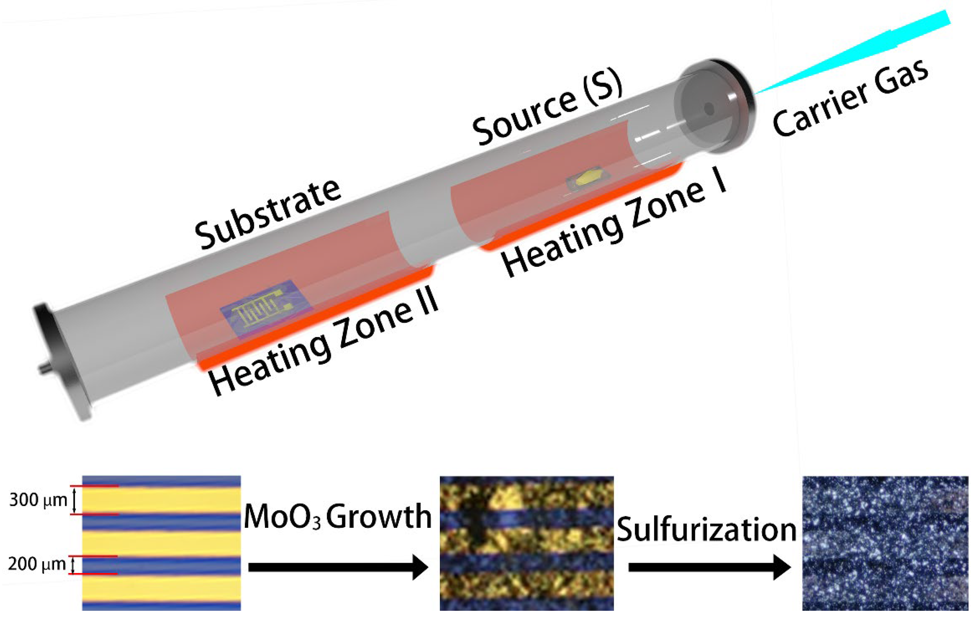
2.1. Synthesis of MoO3
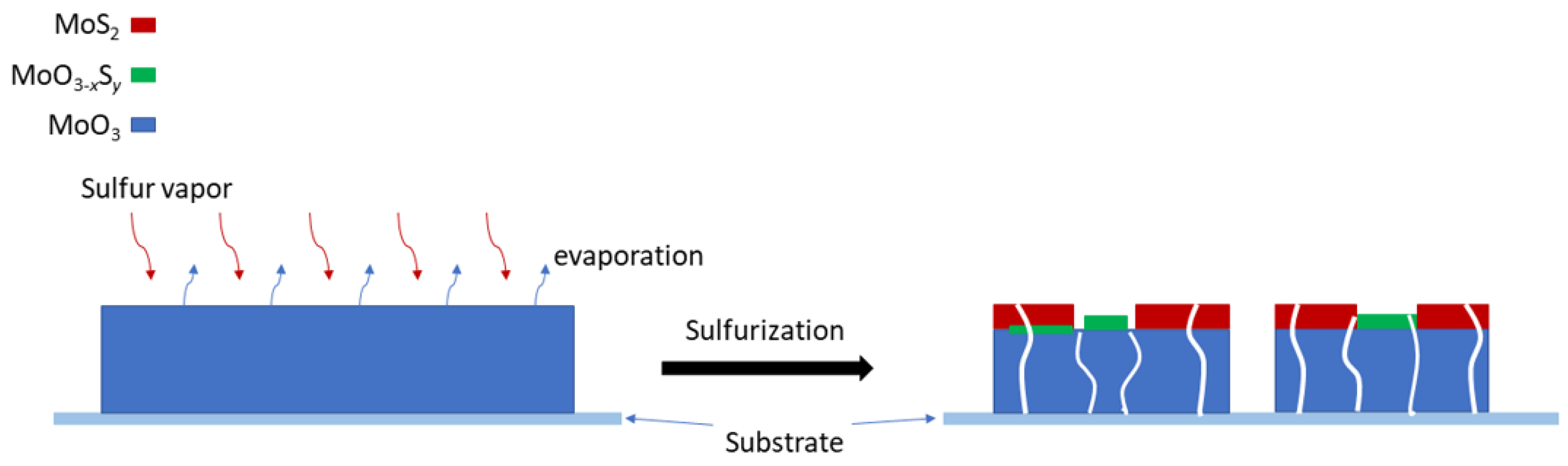
Before the deposition of MoO3 nanoribbons, Au/Ti (100 nm/10 nm) interdigital contact electrodes were deposited on SiO2 (285 nm)/Si substrates through a shadow mask by using electron-beam physical vapor deposition (E-beam PVD). The interdigital electrodes consist of four pairs of electrodes with a width of 300 µm and a spacing of 200 µm (Figure 1). MoO3 nanoribbons were then synthesized via vapor phase transport (VPT) directly on the substrates with pre-patterned electrodes, following our previous reported approach (Figure 1) [27]. In brief, 0.125 g MoO3 (99.95% purity, Strem Chemicals) powder was placed in the center of high-temperature heating Zone I (upstream of the tube) of a dual-zone furnace (LABEC—Split Horizontal Tube Furnace) inside a quartz tube (1000 mm in length, 50 mm in diameter), where the temperature was set to 750 °C (Figure 1). Simultaneously, the SiO2/Si substrate was placed in the low-temperature Zone II (downstream of the tube) with a temperature of 600 °C. Synthetic air (hydrocarbon impurities < 0.1 ppm) was used as the carrier gas with an airflow of 120 sccm.

2.2. Sulfurization

The subsequent sulfurization of the synthesized MoO3 nanoribbons on SiO2/Si substrates was performed in the same quartz tube by replacing the boat with MoO3 powder with 0.6 g sulfur powder (99.3% purity, Ajax Finechem, Sidney, NSW, Australia) at a temperature of 280°. Meanwhile, the substrates with MoO3 nanoribbons were placed in the same location with a temperature of 550°. Pure argon was used as the carrier gas with an airflow of 120 sccm.

2.3. Materials Characterizations

A Leica DM6000 optical microscope (Weltzar, Germany) and Zeiss sigma field emission scanning electron microscope (FESEM, Jena, Germany) were utilized to characterize the surface morphology of the as-grown samples before and after sulfurization. Transmission electron microscopy (TEM) and energy dispersive spectroscopy (EDS) were collected using a JEOL 2100 electron microscope (Tokyo, Japan) to analyze the detailed structure and crystallinity of the as-grown samples after sulfurization. The X-ray diffraction (XRD) pattern was carried out using PANaytical MPD Cu powder XRD with Cu Kα radiation source (Almelo, Netherlands) to study the phase compositions and crystallographic structures of the as-synthesized samples before and after sulfurization. A Raman microscope (Renishaw inVia, Wotton-under-Edge, UK) with an excitation laser of 532 nm in wavelength was employed to study the structural vibration of the samples both before and after sulfurization. The stoichiometry and electronic structure of as-grown samples after sulfurization were studied by X-ray photoelectron spectroscopy (XPS) with a Kratos AXIS Supra photoelectron spectrometer using a monochromatized Al Kα X-ray source (Manchester, UK). The magnetic property of the sulfurated samples was measured by a vibrating-sample magnetometer (VSM) using a Cryogen-free 5 T system (London, UK).

2.4. Characterization of Gas Sensors

A home-built multichannel gas sensing test system was used to evaluate the gas sensing performance of the fabricated gas sensor, shown in Figure S2. The gas sensor was mounted at the top of the ceramic heater providing on operating temperature for the device controlled by an Agilent E3649 power supply (Santa Clara, CA, USA). The test chamber with an internal volume of 1100 mL was coupled to five high precision mass flow controllers (MFC, MKS 1479A, 200 sccm, Andover, MA, USA) capable of supporting five different analytical gases, which were controlled and mixed by a vacuum/mass system controller (MKS 946, Andover, MA, USA). The ratio of flow rates of analytical gases and the dry synthetic air were adjusted by the relative MFC while keeping a constant total flow of 200 sccm inputing to the chamber to obtain the desired concentration of analytical gas for the gas sensing measurements. The conductometric sensing performance of the gas sensor was evaluated by measuring the resistance of the gas sensor exposed in analytical gases at a bias voltage of 1 V by a Keithley 6487 sourcemeter unit (Solon, OH, USA). The sensing response R of the gas sensor to analytical gas is defined as:
R   ( % ) = R g R a R g × 100
where Rg and Ra are the resistance of the sensor exposed in analytical gas and synthetic air, respectively. The polarity of R is hence directly related with the direction of resistance change upon exposure to analytical gas.

3. Results and Discussion

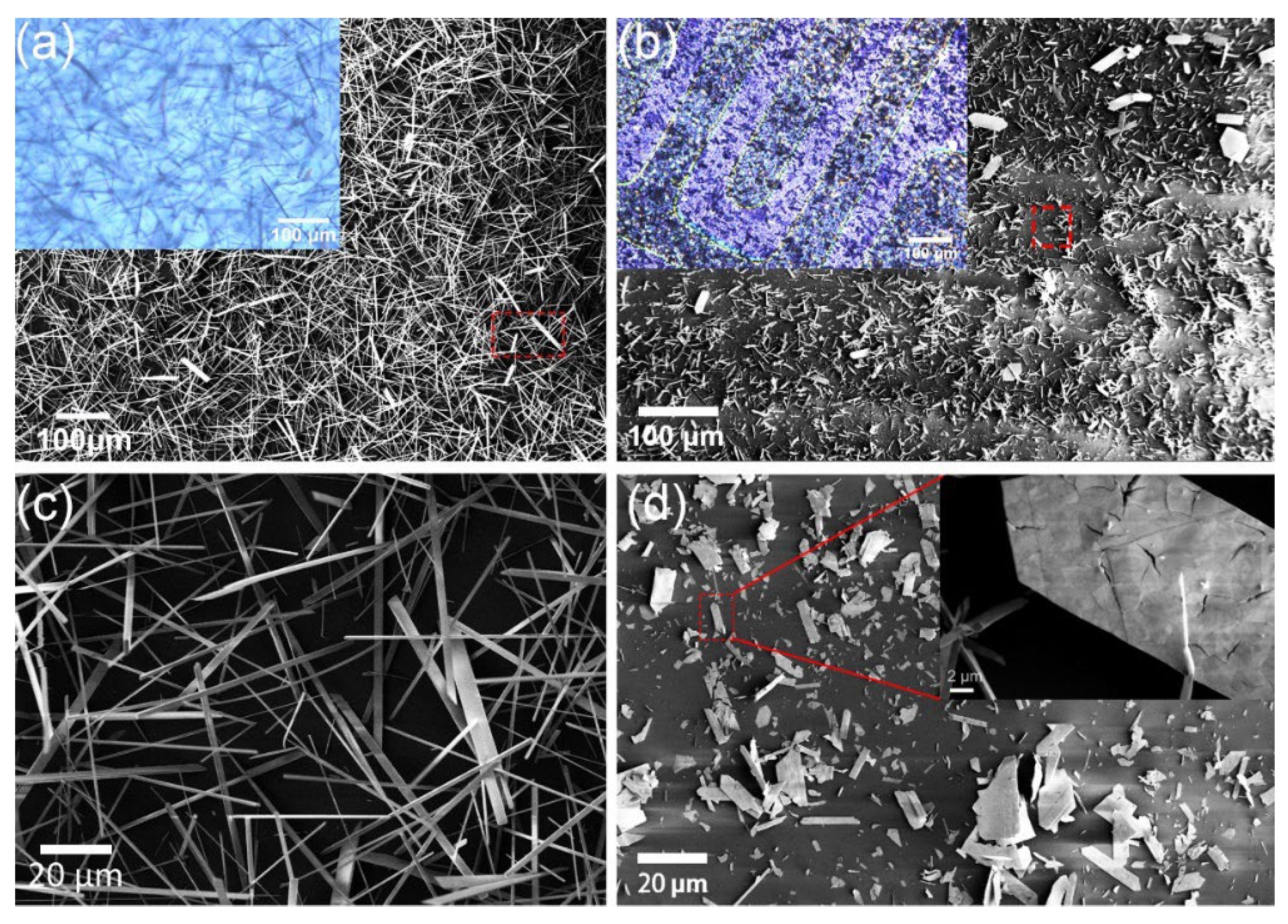
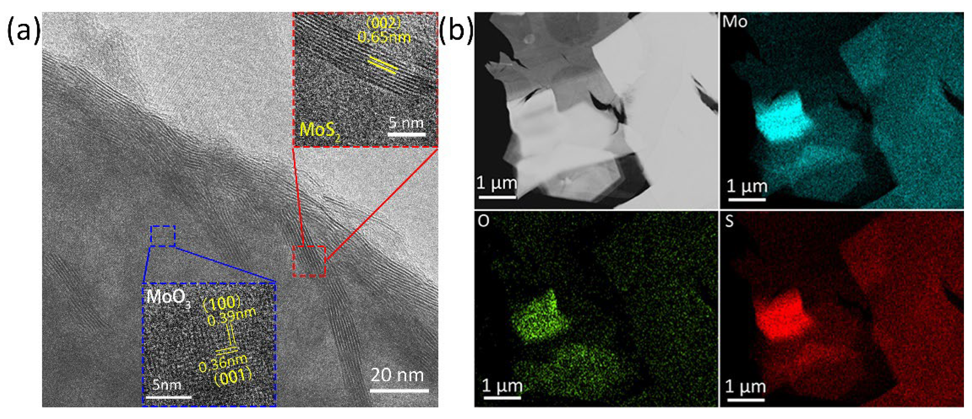
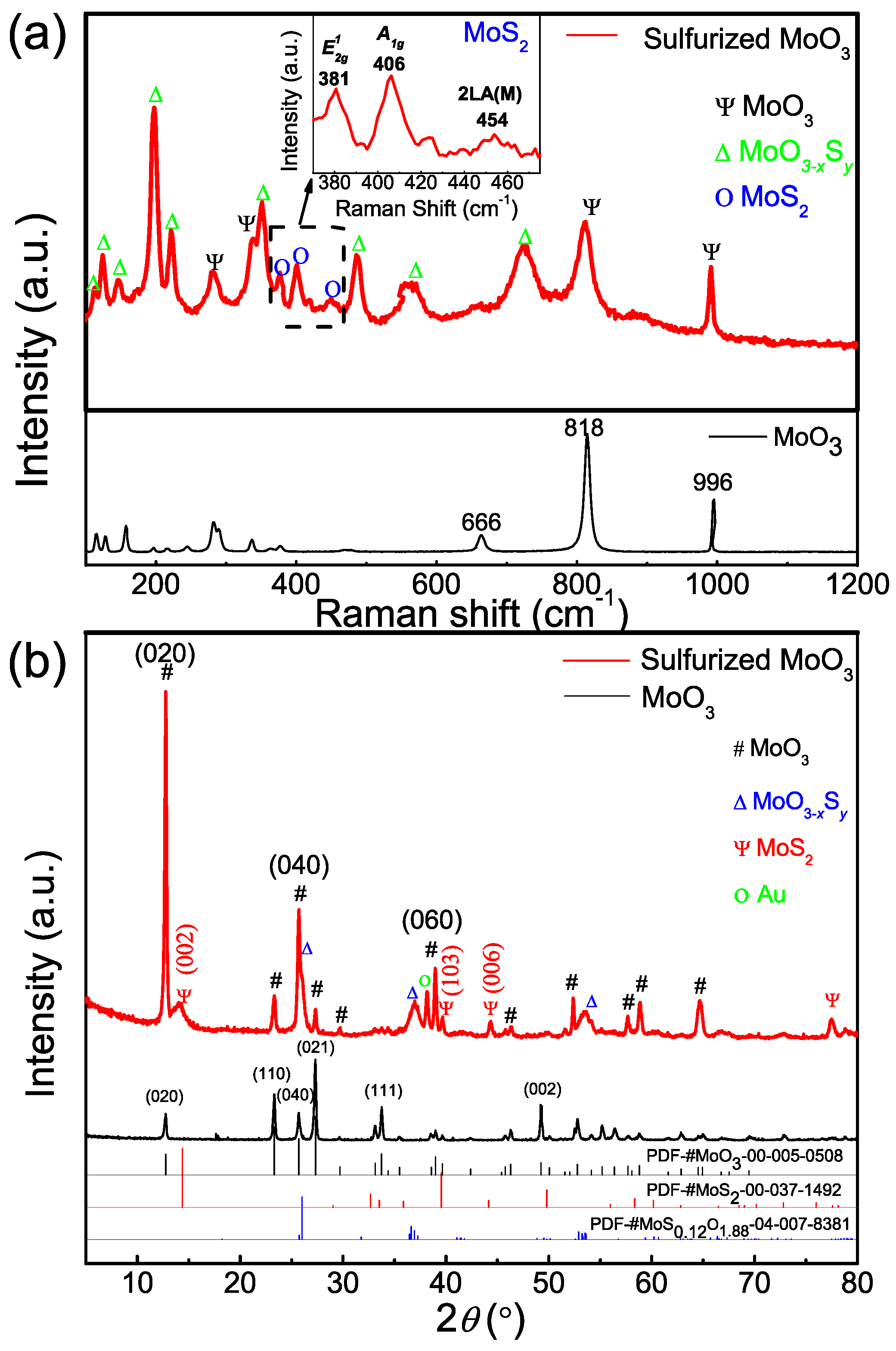
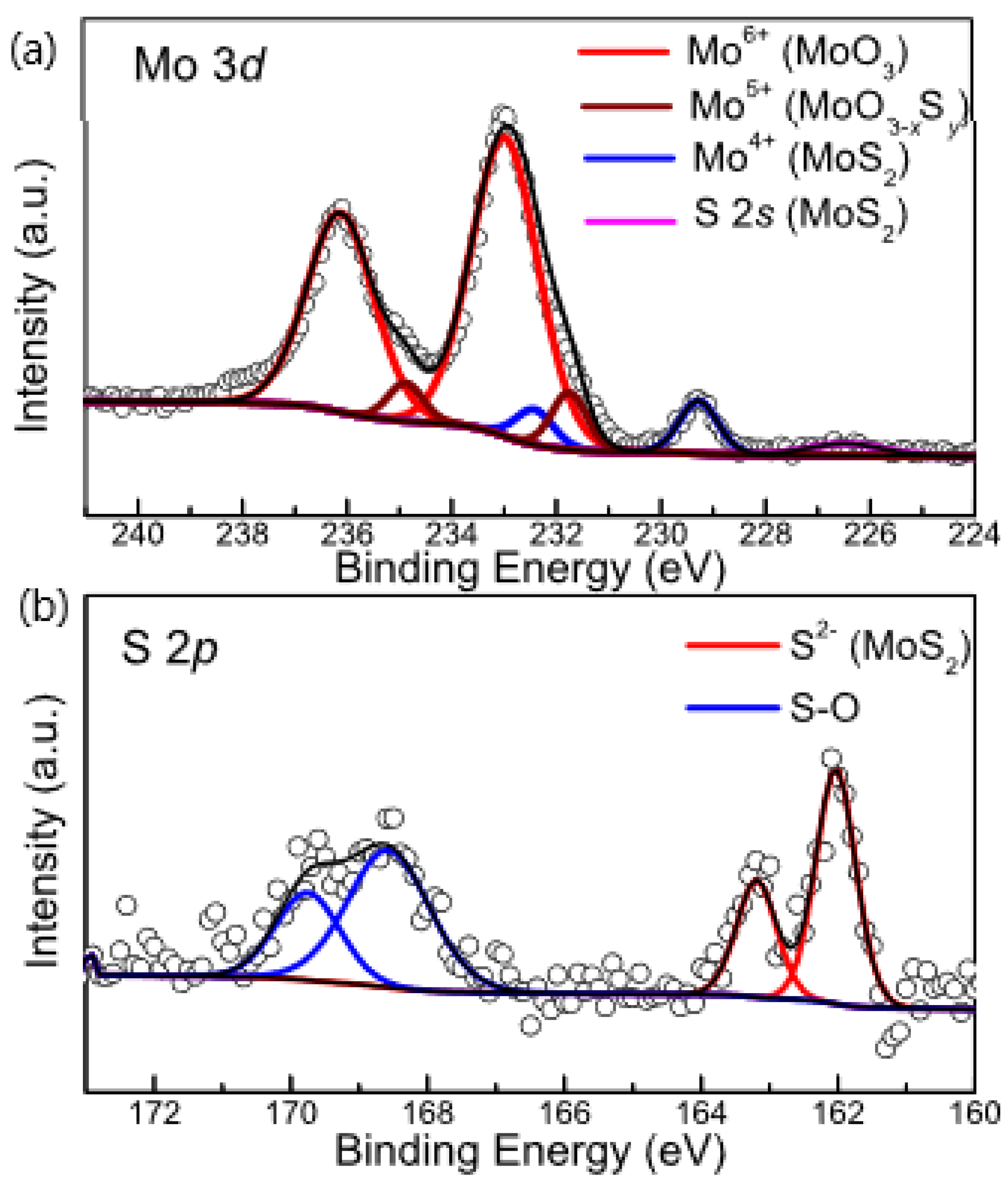
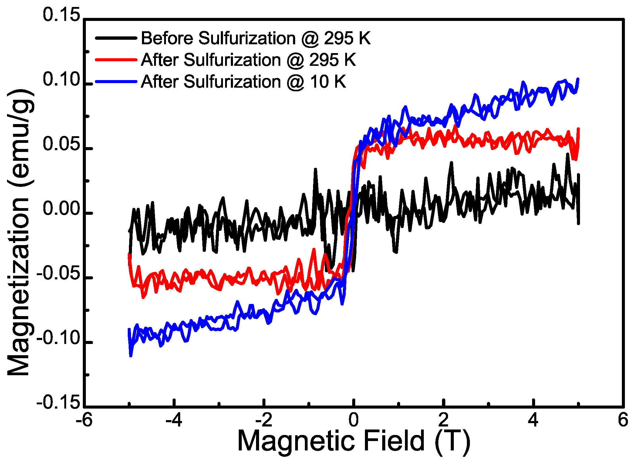
3.1. Materials Characterization

The sulfurization of MoO3 in this work was carried out inside the twin-zone tube furnace as described in the Materials and Methods section by exposing as-grown MoO3 to sulfur vapor. The overall reaction of MoO3 with sulfur vapor during the sulfurization process could be described as [40,41,42,43,44]:
2 M o O 3 + 7 S 2 M o S 2 + 3 S O 2
In this reaction, sulfur atoms progressively remove oxygen from MoO3 by forming gaseous SO2 whilst bonding with Mo to form MoS2. The relative stoichiometric ratio of S to Mo at the substrate surface hence plays a significant role that will directly impact the composites of the product. Incomplete sulfurization can lead to the formation of intermediate molybdenum oxysulfides (MoO3−xSy; 0   x   3 ; 0   y   2 ) described by the following reaction pathway [40]:
2 M o O 3 + ( 2 y + x ) S 2 M o O 3 x S y + x S O 2
Optical microscopy and SEM were employed to characterize the evolution of morphologies of the as-prepared α-MoO3 nanoribbons before and after sulfurization. As shown in Figure 2a, the as-grown α-MoO3 samples grew randomly on the substrate with a high density and possessed a rectangular shape with a typical length of 100 μm and a width of 5 μm (Figure 2c). The morphology of the α-MoO3 nanoribbons is consistent with those reported earlier using the same synthesis condition [27]. The post-sulfurization directly proceeded on the surface of the as-grown α-MoO3 nanoribbons in the sulfur vapor environment. After sulfurization, the samples changed in a few aspects. Firstly, the color of the nanoribbons changed from colorless (i.e., transparent) to dark violet (c.f. optical micrographs in Figure 2a,b), indicating a reduction in the optical bandgap and consistent with the color change expected for the sulfurization of MoO3 [45]. Meanwhile, the density of nanoribbons on the substrate noticeably declined, suggesting the evaporation of MoO3 that consumes the as-grown MoO3 nanoribbons. Secondly, as a result of the sulfurization, the shape of individual nanoribbons changed from elongated rectangles (Figure 2c) to irregular shapes (Figure 2d) and the edges of the crystals appeared to be less well-defined; the surface of the nanoribbons also became rougher with the presence of cracks suggesting that sulfurization alters the crystal structure of MoO3 on the surface leading to lattice mismatch among the hybrid molybdenum compounds. The morphological changes of the sulfurized MoO3 are most likely brought through a complex combination of solid-gas reaction, atomic interdiffusion, evaporation, and deposition [46]. Furthermore, the lateral size of crystals reduced significantly to about 20 μm in length from the original length of about 100 μm.
High-resolution TEM images were collected to further study the structural crystallinity of the sulfurated MoO3 nanoribbons. To prepare TEM samples, substrates with sulfurized MoO3 nanoribbons were placed in ethanol to obtain a well-dispersed solution, after which droplets of the as-prepared solution were drop-casted on lacey-supported 300 mesh copper grids. Figure 3a shows a representative high-resolution transmission electron microscopy (HRTEM) image taken from the edge of sulfurized MoO3. The lattice spacing of 0.36 nm and 0.39 nm corresponds nicely to the (001) and (100) plane of α-MoO3, whereas the lattice spacing of 0.65 nm of layers at the edge of the flake is consistent with the (002) plane of 2H-MoS2, suggesting that the outer layers of α-MoO3 have been partly converted to MoS2 through the sulfurization process. The sulfurization of MoO3 has been further confirmed by the EDS element mapping in Figure 3b which shows an even distribution of S in addition to Mo and O elements.
Raman spectra were also collected to further understand the structural change of MoO3 by sulfurization. As shown in Figure 4a, the Raman spectrum for as-grown MoO3 (black line) exhibits the expected Raman modes for α-MoO3 with a layered structure [47,48]. In particular, it has well-defined Raman features associated with the vibration modes of the oxygen atoms terminating the van der Waals layer at 996 cm−1 (M = O asymmetrical stretching), as well as the stretching mode of the O-Mo bonds at 818 cm−1 for the corner-shared oxygen and at 666 cm−1 for the edge-shared, triply bonded oxygen [49,50]. After sulfurization, the Raman spectrum (red line) displays new peaks in addition to retaining the majority of the characteristic features of MoO3. Most notably, the new peaks at 381 cm−1 and 406 cm−1 are consistent with the characteristic in-plane E 2 g 1 vibration mode and the out-of-plane A 1 g vibration mode of 2H-MoS2, respectively [46,51]. The two Raman peaks have a frequency difference of ~25 cm−1, suggesting that the MoS2 on the surface of MoO3 is multilayer, which is consistent with the HRTEM results. Moreover, the peak 454 cm−1 is assigned to the second order 2LA(M) phonons of MoS2 which are generally present in multilayers of MoS2 [52,53]. There are, however, additional Raman peaks that cannot be exclusively assigned to MoO3 or MoS2, such as strong Raman features at 198, 222, 560, and 730 cm−1, and they are best assigned to the vibration modes of Mo-O and Mo-S bonds in intermediate compound molybdenum oxysulfide (MoO3−xSy) as a result of incomplete sulfurization described in the reaction in Equation (2) [40]. The co-existence of MoO3, MoS2, and the intermediate molybdenum oxysulfide is further corroborated by XRD. Figure 4b shows the XRD patterns of MoO3 before (black line) and after (red line) sulfurization. The intense diffraction peaks of pristine MoO3 can all be indexed to the orthorhombic α-MoO3 (JCPDS Card No. 00-005-0508) including the (0 2 0) and (0 4 0) planes that are characteristic for layered MoO3 [27,54,55]. After sulfurization, the XRD patterns display several additional diffraction peaks including the diffraction peaks with 2θ at 14.4°, 39.5°, and 44.3° corresponding to reflections of the (002), (103), and (006) planes of 2H-MoS2 (JCPDS No. 00-037-1492) [44,56], confirming again the formation of MoS2 on the MoO3 nanoribbons after sulfurization. With the 2θ position of the (002) diffraction peak and the wavelength of Cu Kα line (λ = 0.15418 nm), we can arrive at an interlayer distance of 0.62 nm for MoS2, in good agreement with the d-spacing determined by HRTEM in Figure 3a. The formation of intermediate MoO3−xSy is also supported by the appearance of additional XRD patterns consistent with those from a representative molybdenum oxysulfide MoS0.12O1.88 (JCPDS No. 04-007-8381).
X-ray photoelectron spectroscopy (XPS) characterization was also carried out to determine the compositions and valence states of sulfurized MoO3. The binding energy of XPS spectra was calibrated using adventitious carbon (284.8 eV) as a reference. As shown in the wide survey scan in Figure S1, no other unexpected contaminants were introduced after sulfurization. Figure 5a shows the Mo 3d core-level spectrum which can be deconvoluted to three distinct 3d spin-orbit split doublets fitted by a Voigt line shape. The XPS doublets dominating the high binding energy part of the spectrum at 236.1 eV (Mo 3d3/2) and 233.0 eV (Mo 3d5/2) are assigned to the characteristic Mo6+ state in α-MoO3 [57]. Meanwhile, the Mo 3d doublets positioned at 232.4 and 229.3 eV are consistent with Mo4+ in 2H-MoS2, with the accompanied S 2s peak at 226.5 eV [58,59]. The Mo 3d doublets at 234.9 eV (Mo 3d3/2) and 231.8 eV (Mo 3d5/2), located in between those of the Mo6+ and Mo4+ components, can be ascribed to Mo in MoO3−xSy with a nominal oxidation state of 5+ [24,60]. Correspondingly, S 2p core-level spectrum in Figure 5b shows the S 2p doublets at 163.2 eV (S 2p1/2) and 162.1 eV (S 2p3/2) originating from Mo-S bonds in 2H-MoS2 [35,36,42]. In addition, the peaks at 169.7 eV (S 2p1/2) and 168.6 eV (S 2p3/2) correspond to the S-O bonds both in the intermediate molybdenum oxysulfide and potentially the adsorbed SO2 on the surface of MoO3 as a result of the sulfurization reaction [51,61,62].
The above structural and compositional analysis shows that the sulfurization process induces the formation of MoO3/MoS2 hybrid core-shell structure with the co-existence of incompletely sulfurized oxysulfide intermediates embedded on the surface, as shown schematically in Figure 6. Because of the relatively high temperature of the sulfurization process, the reaction also involves evaporation of MoO3 and re-deposition which consume the initial MoO3 nanoribbons, giving rise to the reduced lateral dimensions and morphological changes of sulfurized MoO3 as discussed above. Although the overall molar ratio of S:MoO3 for the respective sources exceeds the required ratio of 7:2 as in reaction Equation (1) for complete sulfurization, at regions where the high-density MoO3 nanoribbons overlap inhibiting the flow of S vapor to react completely with the outer layers of MoO3, the local effective ratio could be lower leading to the formation of incompletely sulfurized oxysulfide intermediates.
Because NO2 carries a magnetic moment originating from its unpaired valence electron, the magnetic properties of sensing layers could potentially benefit gas sensing performance by enhancing affinity to substrates through magnetic dipole interactions [63]. Although both α-MoO3 and MoS2 are intrinsically non-magnetic, ferromagnetism could be introduced through defects, edges, and non-stoichiometry that induce unpaired electrons in Mo 4d orbitals [64,65,66,67,68]. We therefore measured the magnetic properties of the sulfurated MoO3 samples by VSM with an applied magnetic field in the range of −5 T to 5 T. Figure 7 presents a comparison of the magnetization vs. magnetic field for sulfurized MoO3 samples at room temperature and 10 K and the pristine MoO3. The pristine MoO3 nanoribbons do not exhibit any hysteretic behaviors, consistent with its non-magnetic character with a Mo 4d0 configuration. After sulfurization, the MoS2@MoO3 sample clearly shows ferromagnetic behavior with a specific saturation magnetization (Ms) about 0.05 emu/g at room temperature. The saturation magnetization at 10 K is comparable with that of room temperature, but it further increases slightly with at large magnetic field and did not saturate up to 5 T. This magnetization behavior suggests a combination of ferromagnetic and paramagnetic properties. The observed ferromagnetism is comparable to those reported for defective MoS2 and MoO3 with defect-induced ferromagnetism [64,65,69], and therefore could also originate from the prevalent defects as a result of the sulfurization process. In addition, the edges of MoS2 have been shown to display robust ferromagnetism [70]; the MoS2 nanosheets that cover the surface of MoO3 are expected to give rise to plenty of edge states that enhance the ferromagnetism. Furthermore, the existence of Mo5+ with an unpaired 4d electron (4d1 configuration), as revealed in Figure 5a by XPS, could also provide magnetic moments for the sulfurized MoS2@MoO3 hybrid structures [65]. Lastly, interface-induced ferromagnetism due to interfacial charge transfer [66] could also occur at the MoS2@MoO3 heterointerface by introducing spin magnetic moments into the Mo-4d conduction bands of MoO3. It is worth noting that some of the magnetic moments introduced by sulfurization could be isolated lacking long-range ferromagnetic coupling, giving rise to the observed paramagnetic behavior as mentioned above.

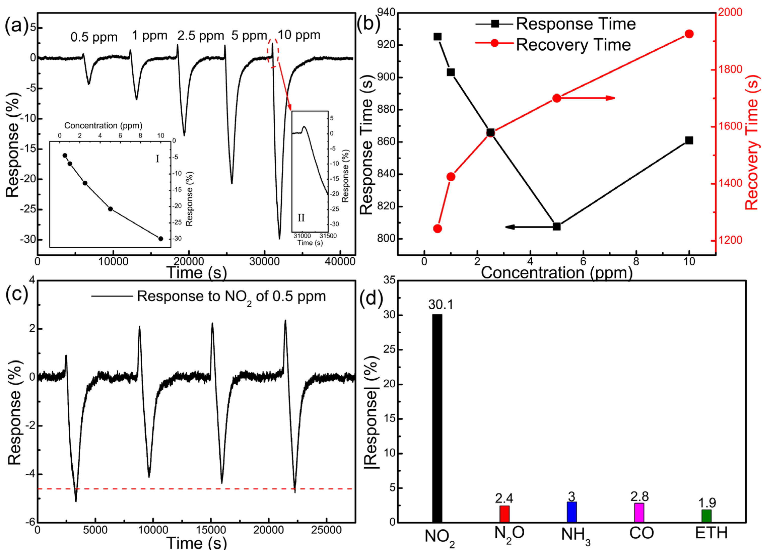
3.2. Gas-Sensing Performance

The gas sensor was fabricated by depositing electrodes on SiO2/Si substrates before α-MoO3 synthesis and the subsequent sulfurization. The gas-sensing performance for NO2, including the dynamic sensing response, response and recovery time, reversibility, and selectivity of the sulfurized MoO3 gas sensors was evaluated with the multichannel gas sensing system (see Figure S2 for the schematics of the sensing test system). All the data for the gas sensing performance were collected at the optimal operating temperature of 125 °C, which was determined by measuring the sensing response as a function of the working temperature of the sensors which was controlled via the ceramic heater underneath. In contrast to positive responses (i.e., increase of resistance) upon exposure to NO2 (typical oxidizing gas) usually displayed by metal oxide conductometric gas sensors including α-MoO3 [10,27,71], the sulfurized device displays a p-type response (i.e., decrease of resistance shown in Figure S3) to NO2 with a concentration in the range of 0.5 ppm to 10 ppm (Figure 8a). The device presents a maximum negative response of −30.1% to NO2 at 10 ppm and a small but noticeable response of −4.3% to 0.5 ppm of NO2. The dependence of response on NO2 concentration is displayed in the inset of Figure 8a which deviates from a linear dependence at high concentration, suggesting the adsorption of NO2 on the surface of sulfurized MoO3 starts to be limited at high concentration. According to the dependence at the low concentrations (inset I of Figure 8a), we can also determine a limit of detection (LOD) of ~0.15 ppm by implementing the IUPAC method [72]. Intriguingly, the sensors display a small positive response upon the input of NO2 before the dominating negative response (inset II of Figure 8a), the origin of which will be discussed below. Figure 8b illustrates the response time (τres) and recovery time (τrec) of the device based on MoS2@MoO3 towards NO2 from 0.5 ppm to 10 ppm at the optimal temperature of 125 °C (also see Figure S4 of Supplementary Material for a detailed presentation of response and recovery time to 10 ppm NO2). In general, the response time decreases with increasing concentration of NO2 (<5 ppm) whereas the recovery time exhibits an opposite trend. Similar dependence has been reported before and is explained with the Freundlich law which dictates a higher diffusion and reaction process with NO2 molecules adsorption (hence faster response dynamics) on the surface at a higher concentration [73,74]. The corresponding desorption is also going to take longer at higher concentration because of the higher number of adsorbed molecules. Intriguingly, the response time at the highest concentration of 10 ppm experiences an increase. It is not exactly clear what causes this anomaly that deviates from the Freundlich law. One possible cause is the initial positive response spike following gas introduction that goes into the calculation of response time (Figure S4). At high NO2 concentration, the positive response spike also increases in magnitude and may cause the negative response to take longer to reach its maximum value. It is worth noting that the nominal response and recovery time of our sensors tend to be overestimated due to the set-up of the sensing test chamber with a large internal volume of 1100 mL. It therefore requires a significantly extended duration to completely replace this volume with the analytical gas at the desired concentration and to purge it away to return to the baseline [27]. However, their dependence on gas concentration (as presented in Figure 8b) is still relevant. The reproducibility and reversibility of the gas sensors are also presented in Figure 8c, in which the device operated with NO2 at 0.5 ppm in four consecutive cycles over an 8 h testing period. The sensors show a reproducible response with a standard deviation of response less than 0.4%. The long-term stability of this sensor was also measured for 8 weeks (Figure S5), in which the response to NO2 decreased from −30.1% to −23% in the first week and then it kept a relatively stable response about −22% in 7 weeks. Lastly, the selectivity of the sulfurized MoO3 sensors was studied by measuring responses to a few interference gases including N2O, NH3, CO, and ethanol (ETH) as shown in Figure 8d. All the responses to the analytical gases were collected at 10 ppm concentration. The MoS2@MoO3 gas sensors clearly exhibit a good selectivity to NO2; we attribute the selectivity to the enhanced magnetic interaction between the paramagnetic NO2 and the ferromagnetic MoS2@MoO3 sensing layer. Upon NO2 adsorption, it induces additional magnetic dipole interaction with the substrate in addition to a surface electric dipole (due to the polar character of NO2), giving rise to a stronger adsorption affinity than the other non-magnetic interference gas molecules.

3.3. Gas-Sensing Mechanism

Both α-MoO3 and MoS2 are typical n-type semiconductors due to the prevalence of anion vacancies (i.e., O and S vacancies) in their pristine structure due to their low formation energy [75,76]. Anion vacancies act as shallow donors in the bandgap leading to n-type conduction behavior. It is well accepted that n-type semiconductors usually respond to oxidizing gas such as NO2 with an increase in resistance (i.e., positive response) as a result of electron depletion in the sensing materials following electron transfer to analytical gas molecules facilitated through the surface adsorbed oxygen ions [77]. The reversal of the response polarity (i.e., decrease in resistance) to NO2 in our MoS2@MoO3 hybrid sensors is therefore intriguing. Due to an extremely high electron affinity of 6.7 eV [75,78], MoO3 is a potent electron acceptor and has been widely used as an interfacial layer to induce or enhance p-type conduction in a wide range of electronic materials including organic semiconductors, diamond, graphene, and TMDCs through the charge transfer doping process [79]. We therefore attribute the negative sensing response to the heterointerface formed between MoO3 and MoS2 with the concomitant interfacial charge exchange. As illustrated in the schematic energy band diagram in Figure 9, MoS2 has an ionization energy of ~5.6 eV [80], and it therefore forms a type-III broken-gap heterojunction with MoO3 with a much deeper conduction band. Because of this extreme band offset, electrons flow spontaneously from the valance band of MoS2 to the conduction band of MoO3 until the Fermi level is equated at thermodynamic equilibrium [81], leading to strong band bending across the interface. The interfacial electron transfer not only depletes the initial free electron carriers in MoS2 but also moves the Fermi energy further to form a MoS2 inversion layer with p-type character [82]. When exposed to air, the hole accumulation layer in MoS2 is enhanced because of further electron transfer from the MoS2 to adsorbed oxygen molecules to form different negative oxygen ion species ( O 2 and O ) [83,84].
O 2 + e O 2
O 2 + 2 e   2 O  
Upon exposure to NO2, the absorbed NO2 molecules directly interact with MoS2 or through the negative oxygen ion species to capture electrons, accompanied by further hole generating in MoS2 [85,86]:
N O 2 ( g a s ) + e N O 2 ( a d s )
N O 2 ( g a s ) + O 2 ( a d s ) + 2 e N O 2 ( a d s ) + 2 O ( a d s )
N O 2 ( g a s ) + O ( a d s ) + 2 e N O 2 ( a d s ) + 2 O ( a d s ) 2
In addition, NO2 can also interact with S vacancies ( V S + + ) at the surface MoS2 [84], again generating holes into the valance band [83,85,86,87].
N O 2 ( a d s ) + V S + + N O 2 ( g a s ) + h +
Consequently, the hole accumulation layer in MoS2 is further enlarged with concomitant increase of hole density, which is translated into a decrease of resistance in response to NO2.
It is worth noting that the resistance change of the n-type α-MoO3 upon NO2 adsorption should remain positive and counteract the resistance change of the p-type MoS2 hole accumulation layer. This may explain the positive response spike immediately following NO2 introduction as in Figure 8a. However, since the thickness of MoS2 is expected to be much lower than that of MoO3 and comparable to the Debye length, its sensing response is maximized to dominate the overall sensing behavior [77], thereby resulting in a net decrease of resistance (i.e., negative response). Similar phenomena have been observed in other materials (e.g., a-RP [88], SnO2 [89], and CuO/ZnO [90]).

4. Conclusions

In conclusion, we report MoS2@MoO3 ferromagnetic heterostructure synthesized by post-sulfurization of α-MoO3 nanoribbons on SiO2/Si substrate. Gas sensors fabricated with the sulfurized MoO3 as sensing layers MoS2@MoO3 display a p-type response towards NO2 with high sensitivity in the range of 0.5 ppm to 10 ppm with a LOD of ~0.15 ppm at the optimal working temperature of 125 °C. The response and recovery time of the sensors, although sluggish due to the nature of the testing apparatus, generally follows the Freundlich model which governs the gas adsorption and diffusion on the surface. The gas sensor also presents good reversibility and impressive selectivity against interfering gases including N2O, NH3, CO, and ETH. The energy band offset at the MoS2-MoO3 heterojunction results in interfacial charge transfer leading to a p-type inversion layer in MoS2, and the gas sensing mechanism can be explained by the charge transfer between the analytical gas molecules and the p-type MoS2 inversion layer at the MoS2-MoO3 heterojunction. The efficient sensing performance for NO2 can be attributed to the enhanced affinity between the paramagnetic NO2 molecules and the ferromagnetic sensing layer. This work demonstrates a promising gas-sensing platform based on MoS2@MoO3 heterostructures and could also have implications for broader applications that utilize the unique electronic and magnetic properties of hybrid 2D metal-oxide/TMDCs heterostructures.

Supplementary Materials

The following supporting information can be downloaded at: https://www.mdpi.com/article/10.3390/nano12081303/s1, Figure S1. XPS wide survey spectrum of sulfurized MoO3, Figure S2. Schematic illustration for the multi-channel gas-sensing characterization system. Inset shows an optical image of the MoS2@MoO3-based gas sensors. Figure S3. Transient resistance of MoS2@MoO3-based gas sensor towards NO2 in range of 0.5 ppm to 10 ppm. Figure S4. Response (0–90%) and recovery time (100–10%) of the MoS2@MoO3-based sensor to 10 ppm NO2 at 125 °C. Figure S5. Long-term stability of MoS2@MoO3 sensors towards 10 ppm NO2 under the operating temperature of 125 °C over a period of 56 days.

Author Contributions

Conceptualization, W.L. and D.-C.Q.; formal analysis, W.L.; funding acquisition, N.M. and D.-C.Q.; investigation, W.L.; methodology, W.L. and M.S.; resources, D.-C.Q.; supervision, T.T., N.M. and D.-C.Q.; visualization, W.L. and K.X.; writing—original draft, W.L.; writing—review and editing, M.S., K.X., T.T. and N.M. All authors have read and agreed to the published version of the manuscript.

Funding

This research is funded by the Australian Research Council (Grant No. FT160100207) (Grant No. DP200102546).

Institutional Review Board Statement

Not applicable.

Informed Consent Statement

Not applicable.

Data Availability Statement

Not applicable.

Acknowledgments

Some of the data reported in this work were obtained at the Central Analytical Research Facility (CARF) at the Queensland University of Technology (QUT). The authors acknowledge the continuous support from QUT through the Centre for Materials Science.

Conflicts of Interest

The authors declare no conflict of interest.

References

  1. Bernstein, J.A.; Alexis, N.; Barnes, C.; Bernstein, I.L.; Nel, A.; Peden, D.; Diaz-Sanchez, D.; Tarlo, S.M.; Williams, P.B.; Bernstein, J.A. Health effects of air pollution. J. Allergy Clin. Immunol. 2004, 114, 1116–1123. [Google Scholar] [CrossRef] [PubMed]
  2. Bernstein, J.A.; Alexis, N.; Bacchus, H.; Bernstein, I.L.; Fritz, P.; Horner, E.; Li, N.; Mason, S.; Nel, A.; Oullette, J.; et al. The health effects of nonindustrial indoor air pollution. J. Allergy Clin. Immunol. 2008, 121, 585–591. [Google Scholar] [CrossRef] [PubMed]
  3. Das, A.; Dost, R.; Richardson, T.; Grell, M.; Morrison, J.J.; Turner, M.L. A Nitrogen Dioxide Sensor Based on an Organic Transistor Constructed from Amorphous Semiconducting Polymers. Adv. Mater. 2007, 19, 4018–4023. [Google Scholar] [CrossRef]
  4. Fernández-Sánchez, J.F.; Fernández, I.; Steiger, R.; Beer, R.; Cannas, R.; Spichiger-Keller, U.E. Second Generation Nanostructured Metal Oxide Matrices to Increase the Thermal Stability of CO and NO2 Sensing Layers Based on Iron(II) Phthalocyanine. Adv. Funct. Mater. 2007, 17, 1188–1198. [Google Scholar] [CrossRef]
  5. Donarelli, M.; Prezioso, S.; Perrozzi, F.; Bisti, F.; Nardone, M.; Giancaterini, L.; Cantalini, C.; Ottaviano, L. Response to NO2 and other gases of resistive chemically exfoliated MoS2-based gas sensors. Sens. Actuator B Chem. 2015, 207, 602–613. [Google Scholar] [CrossRef]
  6. Ji, S.; Wang, H.; Wang, T.; Yan, D. A High-Performance Room-Temperature NO2 Sensor Based on An Ultrathin Heterojunction Film. Adv. Mater. 2013, 25, 1755–1760. [Google Scholar] [CrossRef] [PubMed]
  7. Kumar, S.; Pavelyev, V.; Mishra, P.; Tripathi, N.; Sharma, P.; Calle, F. A review on 2D transition metal di-chalcogenides and metal oxide nanostructures based NO2 gas sensors. Mater. Sci. Semicond. Process. 2020, 107, 104865. [Google Scholar] [CrossRef]
  8. Korotcenkov, G.; Brinzari, V.; Cho, B.K. Conductometric gas sensors based on metal oxides modified with gold nanoparticles: A review. Microchim. Acta 2016, 183, 1033–1054. [Google Scholar] [CrossRef]
  9. Geeta Rani, B.; Saisri, R.; Kailasa, S.; Sai Bhargava Reddy, M.; Maseed, H.; Venkateswara Rao, K. Architectural tailoring of orthorhombic MoO3 nanostructures toward efficient NO2 gas sensing. J. Mater. Sci. 2020, 55, 8109–8122. [Google Scholar] [CrossRef]
  10. Rahman, F.; Zavabeti, A.; Rahman, M.A.; Arash, A.; Mazumder, A.; Walia, S.; Sriram, S.; Bhaskaran, M.; Balendhran, S. Dual Selective Gas Sensing Characteristics of 2D α-MoO3−x via a Facile Transfer Process. ACS Appl. Mater. Interfaces 2019, 11, 40189–40195. [Google Scholar] [CrossRef]
  11. Yang, S.X.; Jiang, C.B.; Wei, S.H. Gas sensing in 2D materials. Appl. Phys. Rev. 2017, 4, 021304. [Google Scholar] [CrossRef]
  12. Di Bartolomeo, A. Emerging 2D Materials and Their Van Der Waals Heterostructures. Nanomaterials 2020, 10, 579. [Google Scholar] [CrossRef] [PubMed] [Green Version]
  13. Joshi, N.; Hayasaka, T.; Liu, Y.; Liu, H.; Oliveira, O.N.; Lin, L. A review on chemiresistive room temperature gas sensors based on metal oxide nanostructures, graphene and 2D transition metal dichalcogenides. Microchim. Acta 2018, 185, 213. [Google Scholar] [CrossRef] [PubMed]
  14. Li, Z.; Qiao, H.; Guo, Z.; Ren, X.; Huang, Z.; Qi, X.; Dhanabalan, S.C.; Ponraj, J.S.; Zhang, D.; Li, J.; et al. High-Performance Photo-Electrochemical Photodetector Based on Liquid-Exfoliated Few-Layered InSe Nanosheets with Enhanced Stability. Adv. Funct. Mater. 2018, 28, 1705237. [Google Scholar] [CrossRef]
  15. Zhang, L.; Khan, K.; Zou, J.; Zhang, H.; Li, Y. Recent Advances in Emerging 2D Material-Based Gas Sensors: Potential in Disease Diagnosis. Adv. Mater. Interfaces 2019, 6, 1901329. [Google Scholar] [CrossRef]
  16. Donarelli, M.; Ottaviano, L. 2D Materials for Gas Sensing Applications: A Review on Graphene Oxide, MoS2, WS2 and Phosphorene. Sensors 2018, 18, 3638. [Google Scholar] [CrossRef] [PubMed] [Green Version]
  17. Novoselov, K.S.; Mishchenko, A.; Carvalho, A.; Castro Neto, A.H. 2D materials and van der Waals heterostructures. Science 2016, 353, aac9439. [Google Scholar] [CrossRef] [Green Version]
  18. Cao, R.; Zhou, B.; Jia, C.; Zhang, X.; Jiang, Z. Theoretical study of the NO, NO2, CO, SO2, and NH3 adsorptions on multi-diameter single-wall MoS2 nanotube. J. Phys. D Appl. Phys. 2015, 49, 045106. [Google Scholar] [CrossRef]
  19. Bermudez, V.M. Computational Study of the Adsorption of NO2 on Monolayer MoS2. J. Phys. Chem. C 2020, 124, 15275–15284. [Google Scholar] [CrossRef]
  20. Zheng, W.; Xu, Y.; Zheng, L.; Yang, C.; Pinna, N.; Liu, X.; Zhang, J. MoS2 Van der Waals p–n Junctions Enabling Highly Selective Room-Temperature NO2 Sensor. Adv. Funct. Mater. 2020, 30, 2000435. [Google Scholar] [CrossRef]
  21. Hau, H.H.; Duong, T.T.H.; Man, N.K.; Thi Viet Nga, T.; Thi Xuan, C.; Thi Thanh Le, D.; Van Toan, N.; Hung, C.M.; Van Duy, N.; Van Hieu, N.; et al. Enhanced NO2 gas-sensing performance at room temperature using exfoliated MoS2 nanosheets. Sens. Actuators A Phys. 2021, 332, 113137. [Google Scholar] [CrossRef]
  22. Kumbhakar, P.; Chowde Gowda, C.; Mahapatra, P.L.; Mukherjee, M.; Malviya, K.D.; Chaker, M.; Chandra, A.; Lahiri, B.; Ajayan, P.M.; Jariwala, D.; et al. Emerging 2D metal oxides and their applications. Mater. Today 2021, 45, 142–168. [Google Scholar] [CrossRef]
  23. Wu, D.; Qi, D.; Liu, J.; Wang, Z.; Hao, Q.; Hong, G.; Liu, F.; Ouyang, F.; Zhang, W. Growth of centimeter-scale single crystal MoO3 ribbons for high performance ultraviolet photodetectors. Appl. Phys. Lett. 2021, 118, 243101. [Google Scholar] [CrossRef]
  24. Duraisamy, S.; Ganguly, A.; Sharma, P.K.; Benson, J.; Davis, J.; Papakonstantinou, P. One-Step Hydrothermal Synthesis of Phase-Engineered MoS2/MoO3 Electrocatalysts for Hydrogen Evolution Reaction. ACS Appl. Nano Mater. 2021, 4, 2642–2656. [Google Scholar] [CrossRef]
  25. He, R.; Lai, H.; Wang, S.; Chen, T.; Xie, F.; Chen, Q.; Liu, P.; Chen, J.; Xie, W. Few-layered vdW MoO3 for sensitive, uniform and stable SERS applications. Appl. Surf. Sci. 2020, 507, 145116. [Google Scholar] [CrossRef]
  26. Du, Y.; He, J.; Hou, G.; Yuan, F. α-MoO3 sheets with high exposed plane reinforced by thermal plasma for stable Li-ion storage. Electrochim. Acta 2020, 334, 135593. [Google Scholar] [CrossRef]
  27. Li, W.; Xing, K.; Liu, P.; Chuang, C.; Lu, Y.-R.; Chan, T.-S.; Tesfamichael, T.; Motta, N.; Qi, D.-C. Ultrasensitive NO2 Gas Sensors Based on Layered α-MoO3 Nanoribbons. Adv. Mater. Technol. 2021, 2100579. [Google Scholar] [CrossRef]
  28. Balendhran, S.; Walia, S.; Nili, H.; Ou, J.Z.; Zhuiykov, S.; Kaner, R.B.; Sriram, S.; Bhaskaran, M.; Kalantar-zadeh, K. Two-Dimensional Molybdenum Trioxide and Dichalcogenides. Adv. Funct. Mater. 2013, 23, 3952–3970. [Google Scholar] [CrossRef]
  29. Malik, R.; Joshi, N.; Tomer, V.K. Advances in the designs and mechanisms of MoO3 nanostructures for gas sensors: A holistic review. Mater. Adv. 2021, 2, 4190–4227. [Google Scholar] [CrossRef]
  30. Wei, Z.; Hai, Z.; Akbari, M.K.; Qi, D.; Xing, K.; Zhao, Q.; Verpoort, F.; Hu, J.; Hyde, L.; Zhuiykov, S. Atomic layer deposition-developed two-dimensional α-MoO3 windows excellent hydrogen peroxide electrochemical sensing capabilities. Sens. Actuators B Chem. 2018, 262, 334–344. [Google Scholar] [CrossRef]
  31. Li, W.; Ou, Q.; Wang, X.; Xing, K.; Tesfamichael, T.; Motta, N.; Qi, D.-C. Large-sized α-MoO3 layered single crystals for superior NO2 gas sensing. Appl. Surf. Sci. 2022, 586, 152793. [Google Scholar] [CrossRef]
  32. Mei, J.; Liao, T.; Sun, Z. 2D/2D Heterostructures: Rational Design for Advanced Batteries and Electrocatalysis. Energy Environ. Mater. 2021, 5, 115–132. [Google Scholar] [CrossRef]
  33. Bag, A.; Lee, N.-E. Gas sensing with heterostructures based on two-dimensional nanostructured materials: A review. J. Mater. Chem. C 2019, 7, 13367–13383. [Google Scholar] [CrossRef]
  34. Guo, S.; Li, X.; Ren, X.; Yang, L.; Zhu, J.; Wei, B. Optical and Electrical Enhancement of Hydrogen Evolution by MoS2@MoO3 Core–Shell Nanowires with Designed Tunable Plasmon Resonance. Adv. Funct. Mater. 2018, 28, 1802567. [Google Scholar] [CrossRef]
  35. Hou, X.; Mensah, A.; Zhao, M.; Cai, Y.; Wei, Q. Facile controlled synthesis of monodispersed MoO3-MoS2 hybrid nanospheres for efficient hydrogen evolution reaction. Appl. Surf. Sci. 2020, 529, 147115. [Google Scholar] [CrossRef]
  36. Chen, Z.; Cummins, D.; Reinecke, B.N.; Clark, E.; Sunkara, M.K.; Jaramillo, T.F. Core-shell MoO3-MoS2 Nanowires for Hydrogen Evolution: A Functional Design for Electrocatalytic Materials. Nano Lett. 2011, 11, 4168–4175. [Google Scholar] [CrossRef]
  37. Zhao, S.; Zha, Z.; Liu, X.; Tian, H.; Wu, Z.; Li, W.; Sun, L.-B.; Liu, B.; Chen, Z. Core-Sheath Structured MoO3@MoS2 Composite for High-Performance Lithium-Ion Battery Anodes. Energy Fuels 2020, 34, 11498–11507. [Google Scholar] [CrossRef]
  38. Singh, S.; Guleria, A.; Singh, N.; Sharma, S. Highly responsive room-temperature ammonia sensing properties of MoS2/MoO3 nano-composite. Mater. Today Proc. 2021, 46, 10732–10735. [Google Scholar] [CrossRef]
  39. Li, J.; Xu, X.; Huang, B.; Lou, Z.; Li, B. Light-Induced In Situ Formation of a Nonmetallic Plasmonic MoS2/MoO3−x Heterostructure with Efficient Charge Transfer for CO2 Reduction and SERS Detection. ACS Appl. Mater. Interfaces 2021, 13, 10047–10053. [Google Scholar] [CrossRef]
  40. Pondick, J.V.; Woods, J.M.; Xing, J.; Zhou, Y.; Cha, J.J. Stepwise Sulfurization from MoO3 to MoS2 via Chemical Vapor Deposition. ACS Appl. Nano Mater. 2018, 1, 5655–5661. [Google Scholar] [CrossRef]
  41. Heo, S.N.; Ishiguro, Y.; Hayakawa, R.; Chikyow, T.; Wakayama, Y. Perspective: Highly ordered MoS2 thin films grown by multi-step chemical vapor deposition process. APL Mater. 2016, 4, 030901. [Google Scholar] [CrossRef] [Green Version]
  42. Guo, Y.; Kang, L.; Song, P.; Zeng, Q.; Tang, B.; Yang, J.; Wu, Y.; Tian, D.; Xu, M.; Zhao, W.; et al. MoO3–MoS2 vertical heterostructures synthesized via one-step CVD process for optoelectronics 2D. Materials 2021, 8, 035036. [Google Scholar] [CrossRef]
  43. Weber, T.; Muijsers, J.C.; van Wolput, J.H.M.C.; Verhagen, C.P.J.; Niemantsverdriet, J.W. Basic reaction steps in the sulfidation of crystalline MoO3 to MoS2, as studied by X-ray photoelectron and infrared emission spectroscopy. J. Phys. Chem. 1996, 100, 14144. [Google Scholar] [CrossRef] [Green Version]
  44. Kumar, R.; Goel, N.; Mishra, M.; Gupta, G.; Fanetti, M.; Valant, M.; Kumar, M. Growth of MoS2–MoO3 Hybrid Microflowers via Controlled Vapor Transport Process for Efficient Gas Sensing at Room Temperature. Adv. Mater. Interfaces 2018, 5, 1800071. [Google Scholar] [CrossRef]
  45. Mohammadbeigi, M.; Jamilpanah, L.; Rahmati, B.; Mohseni, S.M. Sulfurization of planar MoO3 optical crystals: Enhanced Raman response and surface porosity. Mater. Res. Bull. 2019, 118, 110527. [Google Scholar] [CrossRef]
  46. Liu, H.; Lin, M.; Guo, S. Morphological and structural evolutions of α-MoO3 single crystal belts towards MoS2/MoO2 heterostructures upon post-growth thermal vapor sulfurization. Appl. Surf. Sci. 2021, 536, 147956. [Google Scholar] [CrossRef]
  47. Joya, M.R.; Alfonso, J.E.; Moreno, L.C. Photoluminescence and Raman studies of alpha-MoO3 doped with erbium and neodymium. Curr. Sci. 2019, 116, 1690–1695. [Google Scholar] [CrossRef]
  48. Diaz-Droguett, D.E.; El Far, R.; Fuenzalida, V.M.; Cabrera, A.L. In situ-Raman studies on thermally induced structural changes of porous MoO3 prepared in vapor phase under He and H2. Mater. Chem. Phys. 2012, 134, 631–638. [Google Scholar] [CrossRef]
  49. Camacho-López, M.A.; Escobar-Alarcón, L.; Picquart, M.; Arroyo, R.; Córdoba, G.; Haro-Poniatowski, E. Micro-Raman study of the m-MoO2 to α-MoO3 transformation induced by cw-laser irradiation. Opt. Mater. 2011, 33, 480–484. [Google Scholar] [CrossRef]
  50. Silveira, J.V.; Batista, J.A.; Saraiva, G.D.; Mendes Filho, J.; Souza Filho, A.G.; Hu, S.; Wang, X. Temperature dependent behavior of single walled MoO3 nanotubes: A Raman spectroscopy study. Vib. Spectrosc. 2010, 54, 179–183. [Google Scholar] [CrossRef]
  51. Singh, S.; Deb, J.; Sarkar, U.; Sharma, S. MoS2/MoO3 Nanocomposite for Selective NH3 Detection in a Humid Environment. ACS Sustain. Chem. Eng. 2021, 9, 7328–7340. [Google Scholar] [CrossRef]
  52. Windom, B.C.; Sawyer, W.G.; Hahn, D.W. A Raman Spectroscopic Study of MoS2 and MoO3: Applications to Tribological Systems. Tribol. Lett. 2011, 42, 301–310. [Google Scholar] [CrossRef]
  53. Bera, A.; Sood, A.K. Insights into Vibrational and Electronic Properties of MoS2 Using Raman, Photoluminescence, and Transport Studies. In MoS2: Materials, Physics, and Devices; Wang, Z.M., Ed.; Springer International Publishing: Cham, Switzerland, 2014; pp. 155–215. [Google Scholar]
  54. Wang, D.; Li, J.-N.; Zhou, Y.; Xu, D.-H.; Xiong, X.; Peng, R.-W.; Wang, M. Van der Waals epitaxy of ultrathin α-MoO3 sheets on mica substrate with single-unit-cell thickness. Appl. Phys. Lett. 2016, 108, 053107. [Google Scholar] [CrossRef]
  55. Song, L.X.; Xia, J.; Dang, Z.; Yang, J.; Wang, L.B.; Chen, J. Formation, structure and physical properties of a series of α-MoO3 nanocrystals: From 3D to 1D and 2D. Cryst. Eng. Comm. 2012, 14, 2675–2682. [Google Scholar] [CrossRef]
  56. Song, S.; Wang, J.; Peng, T.; Fu, W.; Zan, L. MoS2-MoO3−x hybrid cocatalyst for effectively enhanced H2 production photoactivity of AgIn5S8 nano-octahedrons. Appl. Catal. B Environ. 2018, 228, 39–46. [Google Scholar] [CrossRef]
  57. Szoszkiewicz, R.; Rogala, M.; Dąbrowski, P. Surface-Bound and Volatile Mo Oxides Produced During Oxidation of Single MoS2 Crystals in Air and High Relative Humidity. Materials 2020, 13, 3067. [Google Scholar] [CrossRef] [PubMed]
  58. Hao, S.; Yang, B.; Gao, Y. Chemical vapor deposition growth and characterization of drop-like MoS2/MoO2 granular films. Phys. Status Solidi 2017, 254, 1600245. [Google Scholar] [CrossRef]
  59. Wang, L.; Ji, X.; Wang, T.; Zhang, Q. Novel Red Emission from MoO3/MoS2–MoO2–MoO3 Core–Shell Belt Surface. ACS Appl. Mater. Interfaces 2018, 10, 36297–36303. [Google Scholar] [CrossRef]
  60. Yoon, A.; Kim, J.H.; Yoon, J.; Lee, Y.; Lee, Z. van der Waals Epitaxial Formation of Atomic Layered α-MoO3 on MoS2 by Oxidation. ACS Appl. Mater. Interfaces 2020, 12, 22029–22036. [Google Scholar] [CrossRef]
  61. Kibsgaard, J.; Chen, Z.; Reinecke, B.N.; Jaramillo, T.F. Engineering the surface structure of MoS2 to preferentially expose active edge sites for electrocatalysis. Nat. Mater. 2012, 11, 963–969. [Google Scholar] [CrossRef]
  62. Brown, N.M.D.; Cui, N.; McKinley, A. An XPS study of the surface modification of natural MoS2 following treatment in an RF-oxygen plasma. Appl. Surf. Sci. 1998, 134, 11–21. [Google Scholar] [CrossRef]
  63. Ou, J.Z.; Ge, W.; Carey, B.; Daeneke, T.; Rotbart, A.; Shan, W.; Wang, Y.; Fu, Z.; Chrimes, A.F.; Wlodarski, W.; et al. Physisorption-Based Charge Transfer in Two-Dimensional SnS2 for Selective and Reversible NO2 Gas Sensing. ACS Nano 2015, 9, 10313–10323. [Google Scholar] [CrossRef] [PubMed]
  64. Zhou, X.Y.; Wang, R.; Meng, L.J.; Xu, X.Y.; Hu, J.G.; Pan, J. Achieving half-metallicity in zigzag MoS2 nanoribbon with a sulfur vacancy by edge passivation. J. Phys. D Appl. Phys. 2018, 51, 265005. [Google Scholar] [CrossRef]
  65. Lee, D.J.; Lee, Y.; Kwon, Y.H.; Choi, S.H.; Yang, W.; Kim, D.Y.; Lee, S. Room-Temperature Ferromagnetic Ultrathin α-MoO3:Te Nanoflakes. ACS Nano 2019, 13, 8717–8724. [Google Scholar] [CrossRef] [PubMed]
  66. Brinkman, A.; Huijben, M.; van Zalk, M.; Huijben, J.; Zeitler, U.; Maan, J.C.; van der Wiel, W.G.; Rijnders, G.; Blank, D.H.A.; Hilgenkamp, H. Magnetic effects at the interface between non-magnetic oxides. Nat. Mater. 2007, 6, 493–496. [Google Scholar] [CrossRef]
  67. Shidpour, R.; Manteghian, M. A density functional study of strong local magnetism creation on MoS2 nanoribbon by sulfur vacancy. Nanoscale 2010, 2, 1429–1435. [Google Scholar] [CrossRef]
  68. Rusydi, A.; Dhar, S.; Barman, A.R.; Ariando, n.; Qi, D.C.; Motapothula, M.; Yi, J.B.; Santoso, I.; Feng, Y.P.; Yang, K.; et al. Cationic-vacancy-induced room-temperature ferromagnetism in transparent, conducting anatase Ti1−xTaxO2 (x∼0.05) thin films. Philos. Trans. R. Soc. A Math. Phys. Eng. Sci. 2012, 370, 4927–4943. [Google Scholar] [CrossRef] [Green Version]
  69. Mao, Y.; Li, W.; Sun, X.; Ma, Y.; Xia, J.; Zhao, Y.; Lu, X.; Gan, J.; Liu, Z.; Chen, J.; et al. Room-temperature ferromagnetism in hierarchically branched MoO3 nanostructures. Crystengcomm 2012, 14, 1419–1424. [Google Scholar] [CrossRef]
  70. Botello-Méndez, A.R.; López-Urías, F.; Terrones, M.; Terrones, H. Metallic and ferromagnetic edges in molybdenum disulfide nanoribbons. Nanotechnology 2009, 20, 325703. [Google Scholar] [CrossRef]
  71. Li, Y.; Song, Z.; Li, Y.; Li, S.; Wang, H.; Song, B.; Gao, B.; Du, X. Synthesis of Mo4O11@MoO3 nanobelts and their improved sensing performance to NO2 gas. Mater. Res. Express 2019, 6, 055041. [Google Scholar] [CrossRef]
  72. Analytical Methods, C. Recommendations for the definition, estimation and use of the detection limit. Analyst 1987, 112, 199–204. [Google Scholar] [CrossRef]
  73. Shafiei, M.; Bradford, J.; Khan, H.; Piloto, C.; Wlodarski, W.; Li, Y.; Motta, N. Low-operating temperature NO2 gas sensors based on hybrid two-dimensional SnS2-reduced graphene oxide. Appl. Surf. Sci. 2018, 462, 330–336. [Google Scholar] [CrossRef]
  74. Acharyya, D.; Huang, K.Y.; Chattopadhyay, P.P.; Ho, M.S.; Fecht, H.J.; Bhattacharyya, P. Hybrid 3D structures of ZnO nanoflowers and PdO nanoparticles as a highly selective methanol sensor. Analyst 2016, 141, 2977–2989. [Google Scholar] [CrossRef] [PubMed]
  75. Russell, S.A.O.; Cao, L.; Qi, D.C.; Tallaire, A.; Crawford, K.G.; Wee, A.T.S.; Moran, D.A.J. Surface transfer doping of diamond by MoO3: A combined spectroscopic and Hall measurement study. Appl. Phys. Lett. 2013, 103, 202112. [Google Scholar] [CrossRef] [Green Version]
  76. Li, S.; Ma, Y.; Ouedraogo, N.A.N.; Liu, F.; You, C.; Deng, W.; Zhang, Y. p-/n-Type modulation of 2D transition metal dichalcogenides for electronic and optoelectronic devices. Nano Res. 2022, 15, 123–144. [Google Scholar] [CrossRef]
  77. Miller, D.R.; Akbar, S.A.; Morris, P.A. Nanoscale metal oxide-based heterojunctions for gas sensing: A review. Sens. Actuator B-Chem. 2014, 204, 250–272. [Google Scholar] [CrossRef]
  78. Xing, K.; Xiang, Y.; Jiang, M.; Creedon, D.L.; Akhgar, G.; Yianni, S.A.; Xiao, H.; Ley, L.; Stacey, A.; McCallum, J.C.; et al. MoO3 induces p-type surface conductivity by surface transfer doping in diamond. Appl. Surf. Sci. 2020, 509, 144890. [Google Scholar] [CrossRef] [Green Version]
  79. Xing, K.; Li, W.; Della Gaspera, E.; van Embden, J.; Zhang, L.; Yianni, S.A.; Creedon, D.L.; Wang, T.; McCallum, J.C.; Wang, L.; et al. Surface transfer doping of diamond using solution-processed molybdenum trioxide. Carbon 2021, 175, 20–26. [Google Scholar] [CrossRef]
  80. Keyshar, K.; Berg, M.; Zhang, X.; Vajtai, R.; Gupta, G.; Chan, C.K.; Beechem, T.E.; Ajayan, P.M.; Mohite, A.D.; Ohta, T. Experimental Determination of the Ionization Energies of MoSe2, WS2, and MoS2 on SiO2 Using Photoemission Electron Microscopy. ACS Nano 2017, 11, 8223–8230. [Google Scholar] [CrossRef]
  81. McDonnell, S.; Azcatl, A.; Addou, R.; Gong, C.; Battaglia, C.; Chuang, S.; Cho, K.; Javey, A.; Wallace, R.M. Hole Contacts on Transition Metal Dichalcogenides: Interface Chemistry and Band Alignments. ACS Nano 2014, 8, 6265–6272. [Google Scholar] [CrossRef]
  82. Pal, S.; Mukherjee, S.; Nand, M.; Srivastava, H.; Mukherjee, C.; Jha, S.N.; Ray, S.K. Si compatible MoO3/MoS2 core-shell quantum dots for wavelength tunable photodetection in wide visible range. Appl. Surf. Sci. 2020, 502, 144196. [Google Scholar] [CrossRef]
  83. Hung, C.M.; Vuong, V.A.; Duy, N.V.; An, D.V.; Hieu, N.V.; Kashif, M.; Hoa, N.D. Controlled Growth of Vertically Oriented Trilayer MoS2 Nanoflakes for Room-Temperature NO2 Gas Sensor Applications. Phys. Status Solidi 2020, 217, 2000004. [Google Scholar] [CrossRef]
  84. Yan, W.; Yan, W.; Chen, T.; Xu, J.; Tian, Q.; Ho, D. Size-Tunable Flowerlike MoS2 Nanospheres Combined with Laser-Induced Graphene Electrodes for NO2 Sensing. ACS Appl. Nano Mater. 2020, 3, 2545–2553. [Google Scholar] [CrossRef]
  85. Thang, N.T.; Hong, L.T.; Thoan, N.H.; Hung, C.M.; Van Duy, N.; Van Hieu, N.; Hoa, N.D. Controlled synthesis of ultrathin MoS2 nanoflowers for highly enhanced NO2 sensing at room temperature. RSC Adv. 2020, 10, 12759–12771. [Google Scholar] [CrossRef] [Green Version]
  86. Kwon, H.I. Low-temperature-operated sensitive NO2 gas sensors based on p-type SnO thin-film and thin-film transistors. In Proceedings of the 2020 27th International Workshop on Active-Matrix Flatpanel Displays and Devices (AM-FPD), Kyoto, Japan, 1–4 September 2020; pp. 55–58. [Google Scholar]
  87. Yu, L.; Guo, F.; Liu, S.; Qi, J.; Yin, M.; Yang, B.; Liu, Z.; Fan, X.H. Hierarchical 3D flower-like MoS2 spheres: Post-thermal treatment in vacuum and their NO2 sensing properties. Mater. Lett. 2016, 183, 122–126. [Google Scholar] [CrossRef]
  88. Zhu, Q.; Wang, H.; Yang, J.; Xie, C.; Zeng, D.; Zhao, N. Red Phosphorus: An Elementary Semiconductor for Room-Temperature NO2 Gas Sensing. ACS Sens. 2018, 3, 2629–2636. [Google Scholar] [CrossRef]
  89. Yamada, Y.; Ogita, M. Transient response of resistive-type NO2 sensor on temperature change. Sens. Actuators B Chem. 2003, 93, 546–551. [Google Scholar] [CrossRef]
  90. Yang, L.; Xie, C.; Zhang, G.; Zhao, J.; Yu, X.; Zeng, D.; Zhang, S. Enhanced response to NO2 with CuO/ZnO laminated heterostructured configuration. Sens. Actuators B Chem. 2014, 195, 500–508. [Google Scholar] [CrossRef]
Figure 1. Above: schematic illustration of the post-sulfurization process for MoO3 nanoribbons, the SiO2/Si substrate with pre-patterned interdigital electrodes. Below: the optical images of the device before and after MoO3 synthesis and subsequent sulfurization.
Nanomaterials 12 01303 g001
Figure 2. SEM image of (a) the as-grown α-MoO3 nanoribbons network on SiO2/Si interdigitated substrate, and (b) the sulfurized α-MoO3 nanoribbons. Insets in (a,b) shows the corresponding optical micrographs. The high-resolution SEM image of (c) the as-grown α-MoO3 and (d) the sulfurized α-MoO3. The inset in (d) is a magnified view of an individual sulfurized MoO3 nanoribbon.
Nanomaterials 12 01303 g002
Figure 3. (a) TEM image and (b) EDS element mapping of the sulfurized MoO3 nanoribbons.
Nanomaterials 12 01303 g003
Figure 4. (a) Raman spectra and (b) XRD patterns of MoO3 on SiO2/Si substrate before and after sulfurization.
Nanomaterials 12 01303 g004
Figure 5. XPS spectra of (a) Mo 3d core-levels and (b) S 2p core-levels of sulfurized MoO3 on SiO2/Si substrate.
Nanomaterials 12 01303 g005
Figure 6. A schematic diagram illustrating the sulfurization process of MoO3 nanoribbons.
Nanomaterials 12 01303 g006
Figure 7. Magnetic hysteresis loop of pristine MoO3 and sulfurized MoO3 at different temperatures.
Nanomaterials 12 01303 g007
Figure 8. (a) Dynamic sensing response of the MoS2@MoO3 based sensor to NO2 at concentrations ranging from 0.5 ppm to 10 ppm under the working temperature of 125 °C. Inset I is a plot of the sensing response as a function of NO2 concentration and inset II is the enlarged view of the initial positive response to 10 ppm NO2. (b) Response and recovery time of the MoS2@MoO3-based sensor toward NO2 from 0.5 ppm to 10 ppm at the working temperature of 125 °C. (c) Cyclic response of the sensor toward 0.5 ppm NO2. (d) Selectivity of the sensor in absolute response to NO2, N2O, NH3, CO, and ETH of 10 ppm concentration. Measurements were performed at the optimal operating temperature of 125 °C.
Nanomaterials 12 01303 g008
Figure 9. The energy band diagram of MoS2@MoO3 heterostructure (a) before contact, (b) after contact; (c) gas-sensing mechanism of MoS2@MoO3 heterostructure.
Nanomaterials 12 01303 g009
Publisher’s Note: MDPI stays neutral with regard to jurisdictional claims in published maps and institutional affiliations.

