
Modeling of Optimized Lattice Mismatch by Carbon-Dioxide Laser Annealing on (In, Ga) Co-Doped ZnO Multi-Deposition Thin Films Introducing Designed Bottom Layers

 ,
, 
Abstract
:1. Introduction
2. Materials and Methods
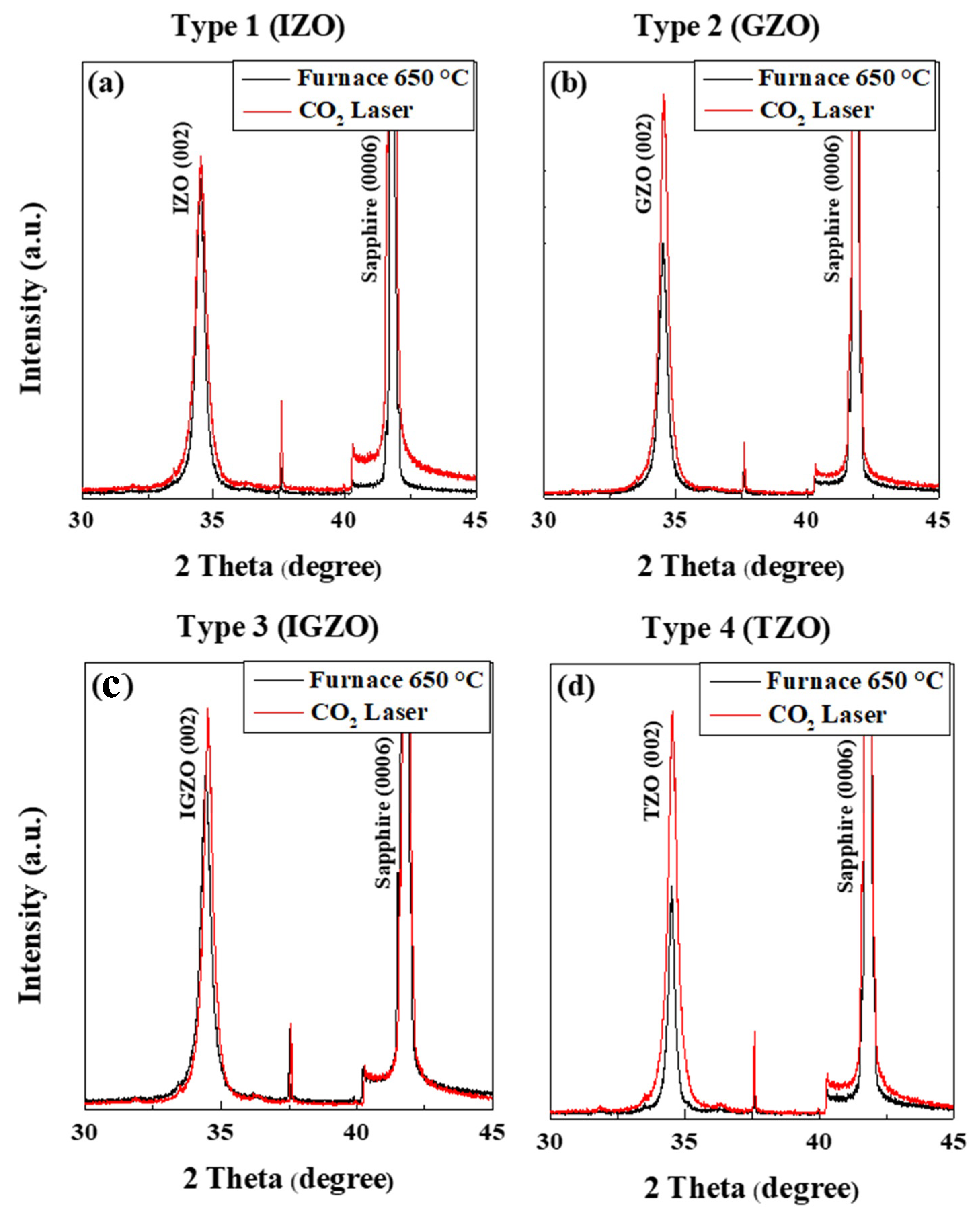
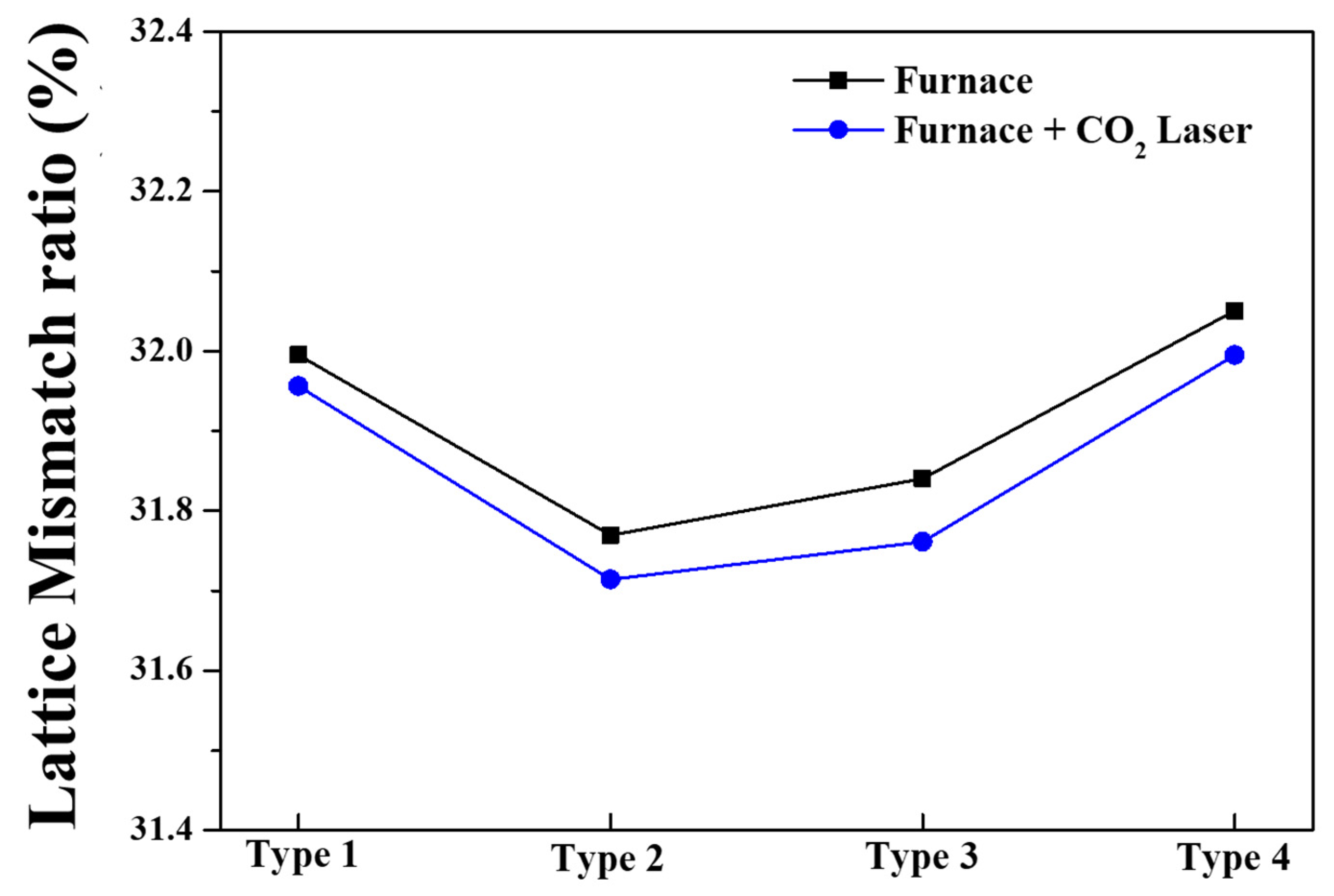
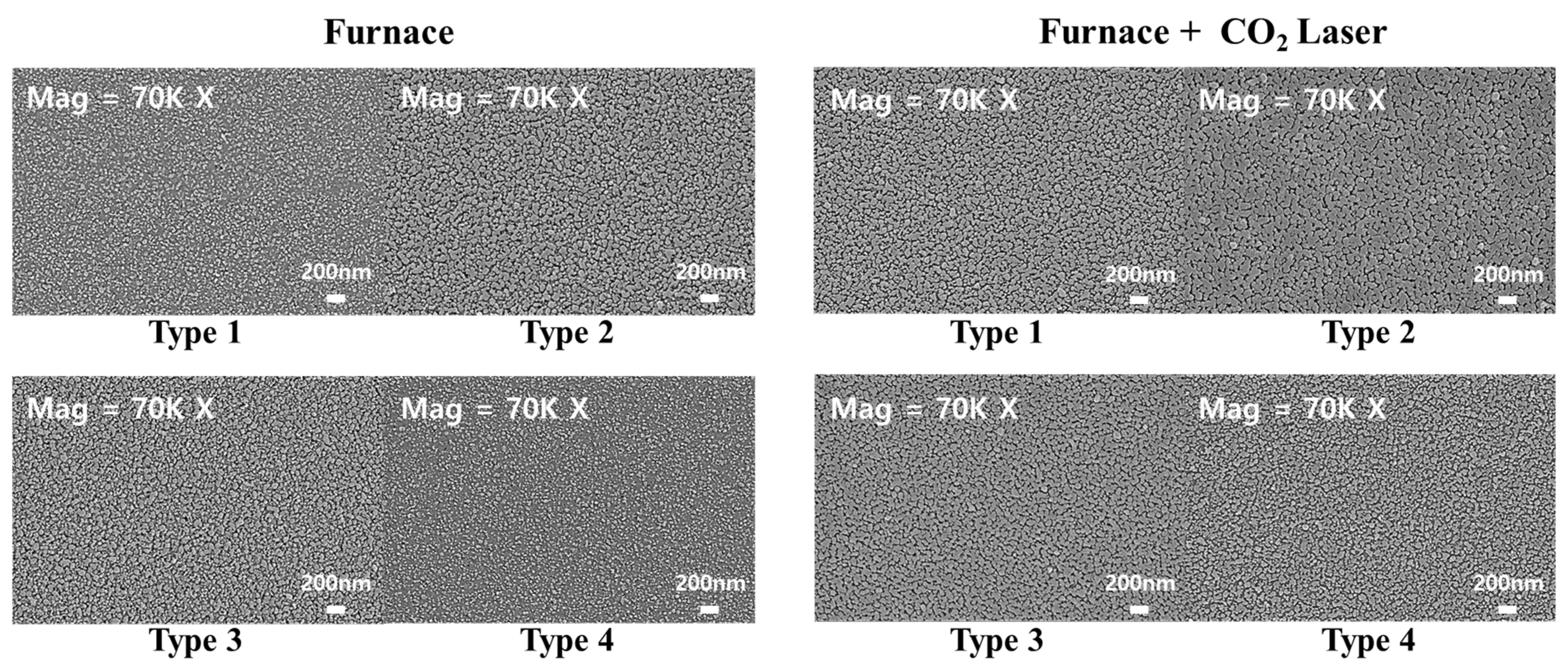
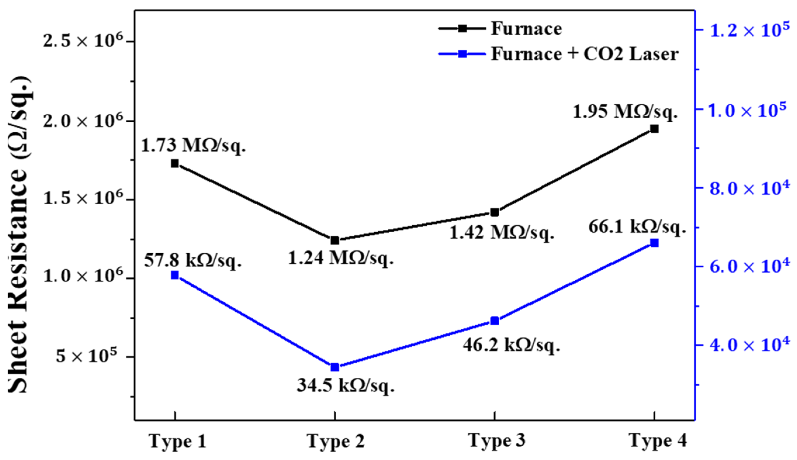
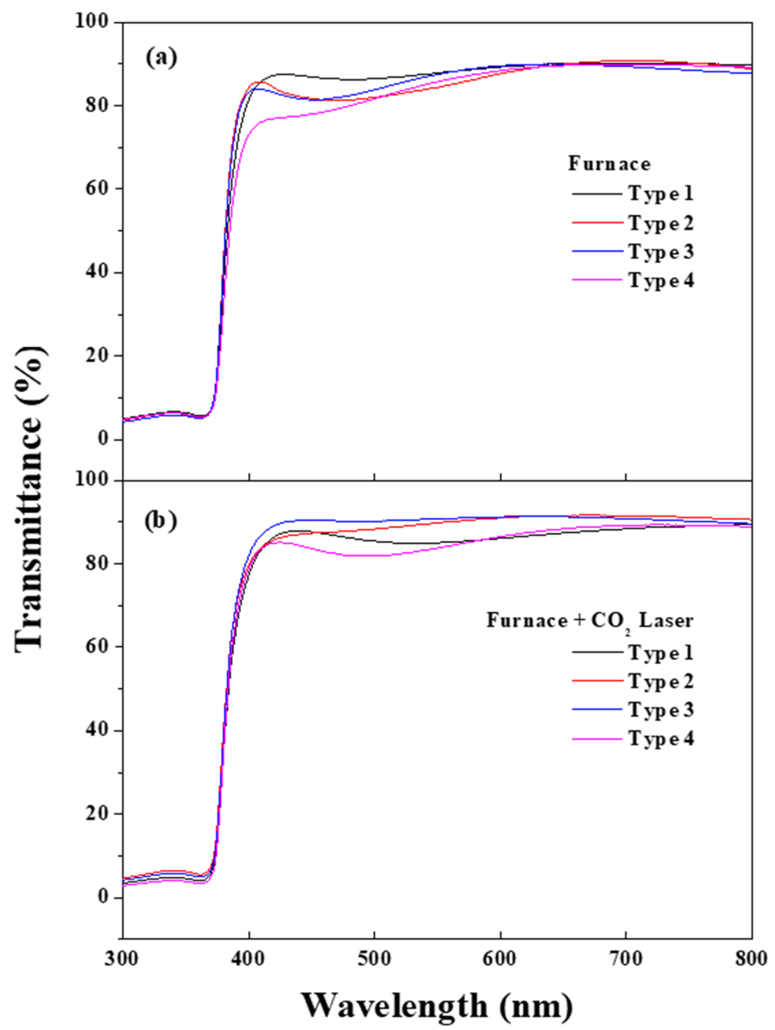
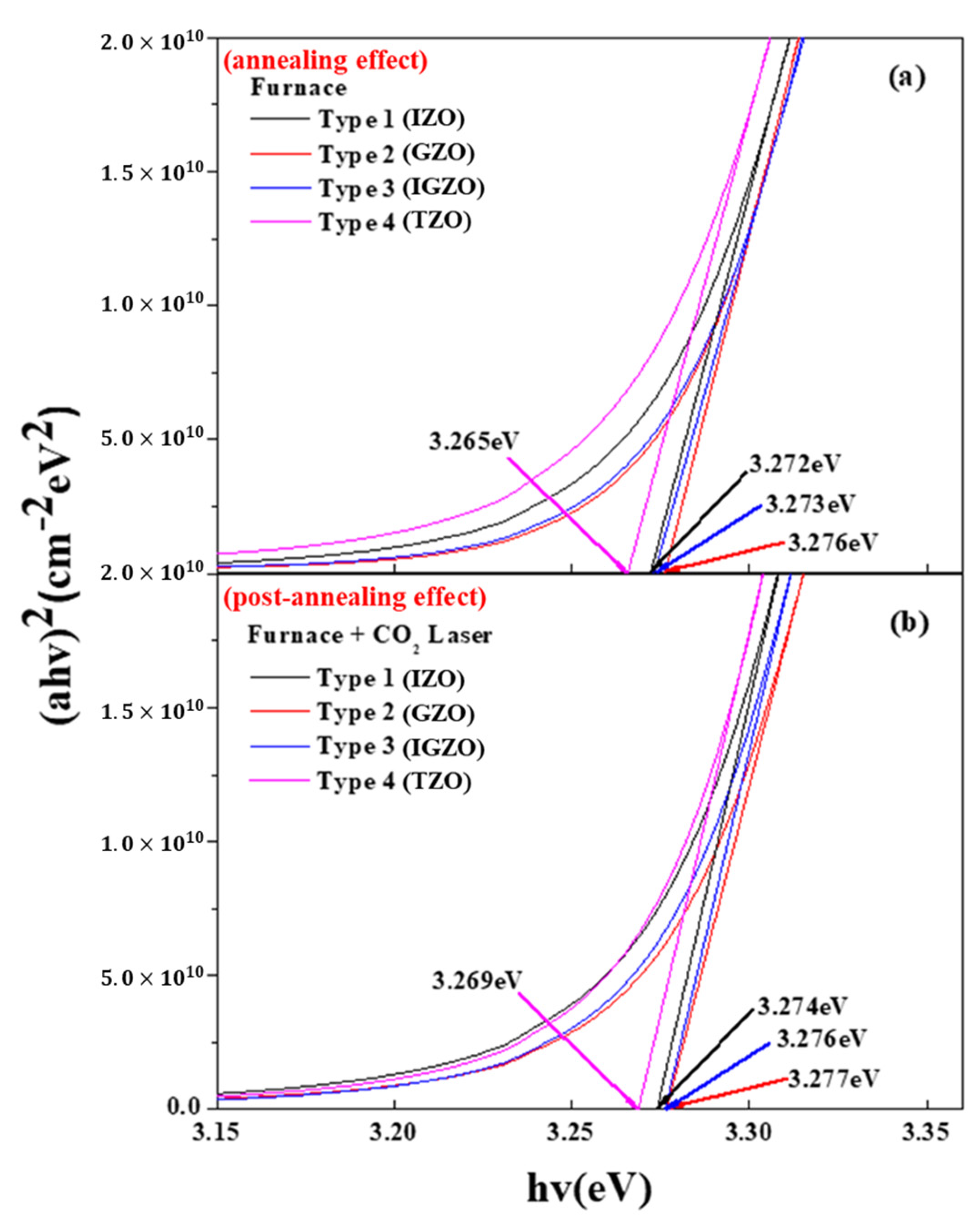
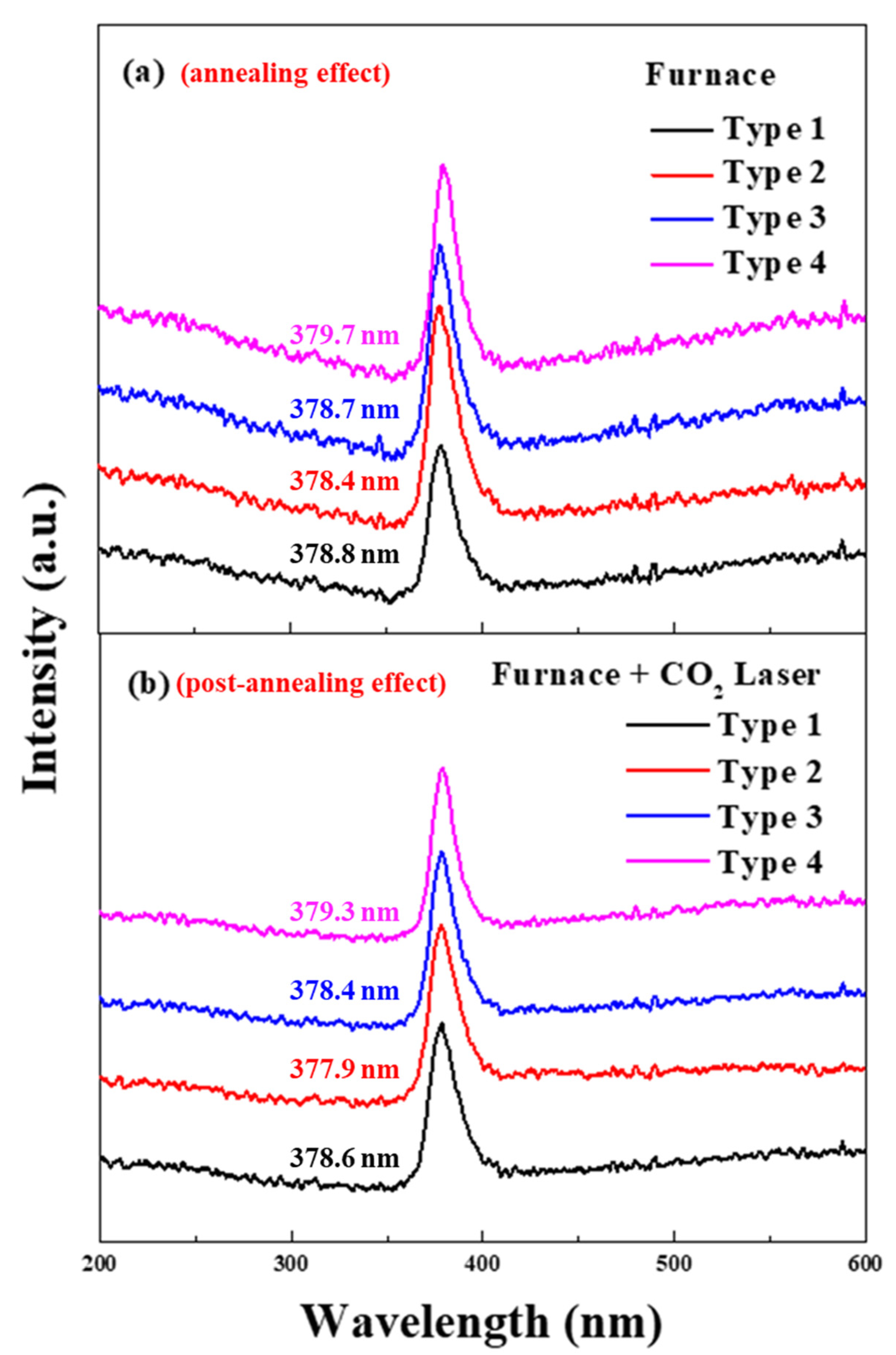
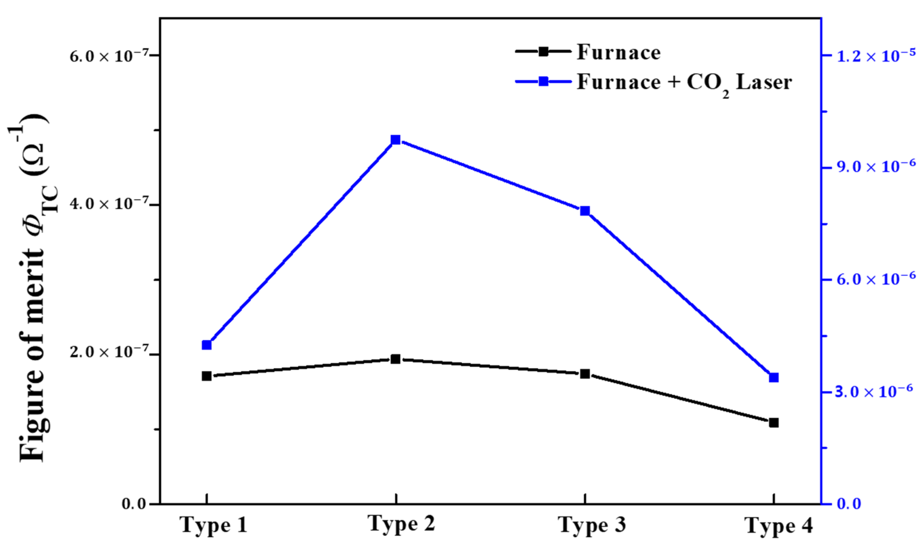
3. Results and Discussion
4. Conclusions
Author Contributions
Funding
Data Availability Statement
Acknowledgments
Conflicts of Interest
References
- Gao, J.; Mu, X.; Li, X.Y.; Meng, Y.; Xu, X.B.; Chen, L.T.; Cui, L.J.; Wu, X.; Geng, H.Z. Modification of carbon nanotube transparent conducting films for electrodes in organic light-emitting diodes. Nanotechnology 2013, 24, 435201. [Google Scholar] [CrossRef] [PubMed]
- Gong, S.C.; Jang, J.G.; Chang, H.J.; Park, J.S. The characteristics of organic light emitting diodes with Al doped zinc oxide grown by atomic layer deposition as a transparent conductive anode. Synth. Met. 2011, 161, 823–827. [Google Scholar] [CrossRef]
- Hu, Y.M.; Li, J.Y.; Chen, N.Y.; Chen, C.Y.; Han, T.C.; Yu, C.C. Effect of sputtering power on crystallinity, intrinsic defects, and optical and electrical properties of Al-doped ZnO transparent conducting thin films for optoelectronic devices. J. Appl. Phys. 2017, 121, 085302. [Google Scholar] [CrossRef]
- Ahmmed, S.; Aktar, A.; Rahman, M.F.; Hossain, J.; Ismail, A.B.M. A numerical simulation of high efficiency CdS/CdTe based solar cell using NiO HTL and ZnO TCO. Optik 2020, 223, 165625. [Google Scholar] [CrossRef]
- Sharmin, A.; Tabassum, S.; Bashar, M.S.; Mahmood, Z.H. Depositions and characterization of sol–gel processed Al-doped ZnO (AZO) as transparent conducting oxide (TCO) for solar cell application. J. Theor. Appl. Phys. 2019, 13, 123–132. [Google Scholar] [CrossRef] [Green Version]
- Dai, H.Q.; Xu, H.; Zhou, Y.N.; Lu, F.; Fu, Z.W. Electrochemical Characteristics of Al2O3-Doped ZnO Films by Magnetron Sputtering. J. Phys. Chem. C 2012, 116, 1519–1525. [Google Scholar] [CrossRef]
- Luna-Arredondo, E.J.; Maldonado, A.; Acosta, R.A.D.R.; Meléndez-Lira, M.A.; Olvera, M.d. Indium-doped ZnO thin films deposited by the sol–gel technique. Thin Solid Films 2005, 490, 132–136. [Google Scholar] [CrossRef]
- Aragones, A.C.; Padros, A.P.; Briones, F.C.; Sanz, F. Study and improvement of aluminium doped ZnO thin films: Limits and advantages. Electrochim. Acta 2013, 109, 117–124. [Google Scholar] [CrossRef]
- Nayak, P.K.; Yang, J.; Kim, J.; Chung, S.; Jeong, J.; Lee, C.; Hong, Y. Spin-coated Ga-doped ZnO transparent conducting thin films for organic light-emitting diodes. J. Phys. D Appl. Phys. 2008, 42, 035102. [Google Scholar] [CrossRef]
- Chang, K.M.; Huang, S.H.; Wu, C.J.; Lin, W.L.; Chen, W.C.; Chi, C.W.; Lin, J.W.; Chang, C.C. Transparent conductive indium-doped zinc oxide films prepared by atmospheric pressure plasma jet. Thin Solid Films 2011, 519, 5114–5117. [Google Scholar] [CrossRef]
- Ungula, J.; Dejene, B.F.; Swart, H.C. Band gap engineering, enhanced morphology and photoluminescence of un-doped, Ga and/or Al-doped ZnO nanoparticles by reflux precipitation method. J. Lumin. 2018, 195, 54–60. [Google Scholar] [CrossRef]
- Kim, J.; Yun, J.; Jee, S.W.; Park, Y.C.; Ju, M.; Han, S.; Kim, Y.; Kim, J.; Anderson, W.A.; Lee, J.; et al. Rapid thermal annealed Al-doped ZnO film for a UV detector. Mater. Lett. 2011, 65, 786–789. [Google Scholar] [CrossRef]
- Gelpey, J.C.; Stump, P.O.; Camm, D. Advantages of rapid optical annealing. Can. J. Phys. 1985, 63, 881–885. [Google Scholar] [CrossRef]
- Maeng, J.; Heo, S.; Jo, G.; Choe, M.; Kim, S.; Hwang, H.; Lee, T. The effect of excimer laser annealing on ZnO nanowires and their field effect transistors. Nanotechnology 2009, 20, 095203. [Google Scholar] [CrossRef]
- He, Q.; Hong, M.H.; Huang, W.M.; Chong, T.C.; Fu, Y.Q.; Du, H.J. CO2 laser annealing of sputtering deposited NiTi shape memory thin films. J. Micromech. Microeng. 2004, 14, 950. [Google Scholar] [CrossRef]
- Lai, M.H.; Lim, K.S.; Islam, M.R.; Gunawardena, D.S.; Yang, H.Z.; Ahmad, H. Effect of CO2 Laser Annealing on Stress Applying Parts Contributing toward Birefringence Modification in Regenerated Grating in Polarization Maintaining Fiber. IEEE Photonics J. 2015, 7, 7801909. [Google Scholar] [CrossRef]
- Miyao, M.; Ohyu, K.; Tokuyama, T. Annealing of phosphorus-ion-implanted silicon using a CO2 laser. Appl. Phys. Lett. 1979, 35, 227. [Google Scholar] [CrossRef]
- Bae, M.-S.; Lee, J.-W.; Koh, J.-H. Synthesis and characterization of multi-phase structure, optical and electrical properties on (Ga–Sn) oxide composite thin film by sol-gel method. Mater. Chem. Phys. 2023, 293, 126960. [Google Scholar] [CrossRef]
- Huang, R.; Robl, W.; Ceric, H.; Detzel, T.; Dehm, G. Stress, Sheet Resistance, and Microstructure Evolution of Electroplated Cu Films During Self-Annealing. IEEE Trans. Device Mater. Reliab. 2010, 10, 47–54. [Google Scholar] [CrossRef]
- Kumarakuru, H.; Cherns, D.; Collins, A.M. The growth and conductivity of nanostructured ZnO films grown on Al-doped ZnO precursor layers by pulsed laser deposition. Ceram. Int. 2014, 40, 8389–8395. [Google Scholar] [CrossRef]
- Drmosh, Q.A.; Rao, S.G.; Yamani, Z.H.; Gondal, M.A. Crystalline nanostructured Cu doped ZnO thin films grown at room temperature by pulsed laser deposition technique and their characterization. Appl. Surf. Sci. 2013, 270, 104–108. [Google Scholar] [CrossRef]
- Garcia-Alonso, D.; Potts, S.E.; van Helvoirt, C.A.A.; Verheijen, M.A.; Kessels, W.M.M. Atomic layer deposition of B-doped ZnO using triisopropyl borate as the boron precursor and comparison with Al-doped ZnO. J. Mater. Chem. C 2015, 3, 3095–3107. [Google Scholar] [CrossRef] [Green Version]
- Lin, M.L.; Huang, J.M.; Ku, C.S.; Lin, C.M.; Lee, H.Y.; Juang, J.Y. High mobility transparent conductive Al-doped ZnO thin films by atomic layer deposition. J. Alloys Compd. 2017, 727, 565–571. [Google Scholar] [CrossRef]
- An, H.R.; Ahn, H.J.; Park, J.W. High-quality, conductive, and transparent Ga-doped ZnO films grown by atmospheric-pressure chemical-vapor deposition. Ceram. Int. 2015, 41, 2253–2259. [Google Scholar] [CrossRef]
- Huang, Y.C.; Weng, L.W.; Uen, W.Y.; Lan, S.M.; Li, Z.Y.; Liao, S.M.; Lin, T.Y.; Yang, T.N. Annealing effects on the p-type ZnO films fabricated on GaAs substrate by atmospheric pressure metal organic chemical vapor deposition. J. Alloys Compd. 2011, 509, 1980–1983. [Google Scholar] [CrossRef]
- Bae, M.S.; Kim, S.H.; Baek, J.S.; Koh, J.H. Comparative Study of High-Temperature Annealed and RTA Process β-Ga2O3 Thin Film by Sol–Gel Process. Coatings 2021, 11, 1220. [Google Scholar] [CrossRef]
- Aydın, H.; Aydın, C.; Al-Ghamdi, A.A.; Farooq, W.A.; Yakuphanoglu, F. Refractive index dispersion properties of Cr-doped ZnO thin films by sol–gel spin coating method. Optik 2016, 127, 1879–1883. [Google Scholar] [CrossRef]
- Bhati, V.S.; Ranwa, S.; Fanetti, M.; Valant, M.; Kumar, M. Efficient hydrogen sensor based on Ni-doped ZnO nanostructures by RF sputtering. Sens. Actuators B Chem. 2018, 255, 588–597. [Google Scholar] [CrossRef]
- Kamaruddin, S.A.; Chan, K.Y.; Yow, H.K.; Sahdan, M.Z.; Saim, H.; Knipp, D. Zinc oxide films prepared by sol–gel spin coating technique. Appl. Phys. A 2011, 104, 263–268. [Google Scholar] [CrossRef]
- Kacher, J.; Landon, C.; Adams, B.L.; Fullwood, D. Bragg’s Law diffraction simulations for electron backscatter diffraction analysis. Ultramicroscopy 2009, 109, 1148–1156. [Google Scholar] [CrossRef]
- AnilKumar, M.R.; Ravikumar, C.R.; Nagaswarupa, H.P.; Purshotam, B.; AbdisaGonfa, B.; AnandaMurthy, H.C.; KedirSabir, F.; Tadesse, S. Evaluation of bi-functional applications of ZnO nanoparticles prepared by green and chemical methods. J. Environ. Chem. Eng. 2019, 7, 103468. [Google Scholar]
- Iwanaga, H.; Kunishige, A.; Takeuchi, S. Anisotropic thermal expansion in wurtzite-type crystals. J. Mater. Sci. 2000, 35, 2451–2454. [Google Scholar] [CrossRef]
- Shen, W.; Hertz, J.L. Ionic conductivity of YSZ/CZO multilayers with variable lattice mismatch. J. Mater. Chem. A 2015, 3, 2378–2386. [Google Scholar] [CrossRef] [Green Version]
- Fons, P.; Iwata, K.; Niki, S.; Yamada, A.; Matsubara, K. Growth of high-quality epitaxial ZnO films on α-Al2O3. J. Cryst. Growth 1999, 201–202, 627–632. [Google Scholar] [CrossRef]
- Wen, K.; Lv, W.; He, W. Interfacial lattice-strain effects on improving the overall performance of micro-solid oxide fuel cells. J. Mater. Chem. A 2015, 3, 20031–20050. [Google Scholar] [CrossRef]
- Goel, S.; Sinha, N.; Yadav, H.; Joseph, A.J.; Kumar, B. 2D porous nanosheets of Y-doped ZnO for dielectric and ferroelectric applications. J. Mater. Sci. Mater. Electron. 2018, 29, 13818–13832. [Google Scholar] [CrossRef]
- Sundaram, P.S.; Sangeetha, T.; Rajakarthihan, S.; Vijayalaksmi, R.; Elangovan, A.; Arivazhagan, G. XRD structural studies on cobalt doped zinc oxide nanoparticles synthesized by coprecipitation method: Williamson-Hall and size-strain plot approaches. Phys. B Condens. Matter 2020, 595, 412342. [Google Scholar] [CrossRef]
- Tao, X.Y.; Fsaifes, I.; Koncar, V.; Dufour, C.; Lepers, C.; Hay, L.; Capoen, B.; Bouazaoui, M. CO2 laser-induced crystallization of sol–gel-derived indium tin oxide films. Appl. Phys. A 2009, 96, 741–749. [Google Scholar] [CrossRef]
- Wu, H.C.; Peng, Y.C.; Chen, C.C. Effects of Ga concentration on electronic and optical properties of Ga-doped ZnO from first principles calculations. Opt. Mater. 2013, 35, 509–515. [Google Scholar] [CrossRef]
- Vladimirov, I.; Kühn, M.; Geßner, T.; May, F.; Weitz, R.T. Energy barriers at grain boundaries dominate charge carrier transport in an electron-conductive organic semiconductor. Sci. Rep. 2018, 8, 14868. [Google Scholar] [CrossRef] [Green Version]
- Kim, C.E.; Moon, P.; Kim, S.; Myoung, J.M.; Jang, H.W.; Bang, J.; Yun, I. Effect of carrier concentration on optical bandgap shift in ZnO:Ga thin films. Thin Solid Films 2010, 518, 6304–6307. [Google Scholar] [CrossRef]
- Gürbüz, O.; Kurt, İ.; Çalışkan, S.; Güner, S. Influence of Al concentration and annealing temperature on structural, optical, and electrical properties of Al co-doped ZnO thin films. Appl. Surf. Sci. 2015, 349, 549–560. [Google Scholar] [CrossRef]
- Hussain, N.; Liang, T.; Zhang, Q.; Anwar, T.; Huang, Y.; Lang, J.; Huang, K.; Wu, H. Ultrathin Bi Nanosheets with Superior Photoluminescence. Small 2017, 13, 1701349. [Google Scholar] [CrossRef] [PubMed]
- Haacke, G. New Figure of merit for transparent conductors. J. Appl. Phys. 1976, 47, 4086. [Google Scholar] [CrossRef]


| Materials | (002) Peak Angle (2 θ) (F/FL) | FWHM (F/FL) | Lattice Parameter c (Å) (F/FL) | Lattice Parameter A (Å) (F/FL) |
|---|---|---|---|---|
| IZO | 34.5927/34.5723 | 0.44/0.41 | 5.1797/5.1827 | 3.2329/3.2348 |
| GZO | 34.4744/34.4458 | 0.51/0.22 | 5.1969/5.2011 | 3.2437/3.2463 |
| IGZO | 34.5112/34.4703 | 0.47/0.33 | 5.1915/5.1975 | 3.2403/3.2441 |
| TZO | 34.6213/34.5927 | 0.63/0.32 | 5.1755/5.1797 | 3.2303/3.2329 |
| Type | Crystallite Size (nm) (F) | Crystallite Size (nm) (FL) | Crystallite Size Difference (nm) |
|---|---|---|---|
| Type 1 | 21.16 | 21.82 | 0.66 |
| Type 2 | 21.44 | 22.81 | 1.37 |
| Type 3 | 21.32 | 22.09 | 0.77 |
| Type 4 | 19.95 | 20.56 | 0.61 |
| Type | Peak Wavelength (nm) (F) | Peak Wavelength (nm) (FL) | Energy Band Gap (eV) (F) | Energy Band Gap (eV) (FL) |
|---|---|---|---|---|
| Type 1 | 378.8 | 378.6 | 3.271 | 3.274 |
| Type 2 | 378.4 | 377.9 | 3.277 | 3.280 |
| Type 3 | 378.7 | 378.4 | 3.274 | 3.277 |
| Type 4 | 379.7 | 379.3 | 3.265 | 3.268 |
Disclaimer/Publisher’s Note: The statements, opinions and data contained in all publications are solely those of the individual author(s) and contributor(s) and not of MDPI and/or the editor(s). MDPI and/or the editor(s) disclaim responsibility for any injury to people or property resulting from any ideas, methods, instructions or products referred to in the content. |
© 2022 by the authors. Licensee MDPI, Basel, Switzerland. This article is an open access article distributed under the terms and conditions of the Creative Commons Attribution (CC BY) license (https://creativecommons.org/licenses/by/4.0/).
Share and Cite
Yun, J.; Bae, M.-S.; Baek, J.S.; Kim, T.W.; Kim, S.-J.; Koh, J.-H. Modeling of Optimized Lattice Mismatch by Carbon-Dioxide Laser Annealing on (In, Ga) Co-Doped ZnO Multi-Deposition Thin Films Introducing Designed Bottom Layers. Nanomaterials 2023, 13, 45. https://doi.org/10.3390/nano13010045
Yun J, Bae M-S, Baek JS, Kim TW, Kim S-J, Koh J-H. Modeling of Optimized Lattice Mismatch by Carbon-Dioxide Laser Annealing on (In, Ga) Co-Doped ZnO Multi-Deposition Thin Films Introducing Designed Bottom Layers. Nanomaterials. 2023; 13(1):45. https://doi.org/10.3390/nano13010045
Chicago/Turabian StyleYun, Jaeyong, Min-Sung Bae, Jin Su Baek, Tae Wan Kim, Sung-Jin Kim, and Jung-Hyuk Koh. 2023. "Modeling of Optimized Lattice Mismatch by Carbon-Dioxide Laser Annealing on (In, Ga) Co-Doped ZnO Multi-Deposition Thin Films Introducing Designed Bottom Layers" Nanomaterials 13, no. 1: 45. https://doi.org/10.3390/nano13010045
APA StyleYun, J., Bae, M.-S., Baek, J. S., Kim, T. W., Kim, S.-J., & Koh, J.-H. (2023). Modeling of Optimized Lattice Mismatch by Carbon-Dioxide Laser Annealing on (In, Ga) Co-Doped ZnO Multi-Deposition Thin Films Introducing Designed Bottom Layers. Nanomaterials, 13(1), 45. https://doi.org/10.3390/nano13010045