Communication

A Novel Atomic-Level Post-Etch-Surface-Reinforcement Process for High-Performance p-GaN Gate HEMTs Fabrication

1
State Key Laboratory of ASIC and System, Shanghai Institute of Intelligent Electronics & Systems, School of Microelectronics, Fudan University, Shanghai 200433, China
2
Imperial College London, London SW7 2AZ, UK
3
Shanghai Integrated Circuit Manufacturing Innovation Center Co., Ltd., Shanghai 200433, China
*
Authors to whom correspondence should be addressed.
Nanomaterials 2023, 13(16), 2275; https://doi.org/10.3390/nano13162275
Submission received: 25 July 2023 / Revised: 4 August 2023 / Accepted: 4 August 2023 / Published: 8 August 2023

Abstract

:
A novel atomic-level post-etch-surface-reinforcement (PESR) process is developed to recover the p-GaN etching induced damage region for high performance p-GaN gate HEMTs fabrication. This process is composed of a self-limited surface modification step with O2 plasma, following by an oxide removal step with BCl3 plasma. With PESR process, the AlGaN surface morphology after p-GaN etching was comparable to the as-epitaxial level by AFM characterization, and the AlGaN lattice crystallization was also recovered which was measured in a confocal Raman system. The electrical measurement further confirmed the significant improvement of AlGaN surface quality, with one-order of magnitude lower surface leakage in a metal-semiconductor (MS) Schottky-diode and 6 times lower interface density of states (Dit) in a MIS C-V characterization. The XPS analysis of Al2O3/AlGaN showed that the p-GaN etching induced F-byproduct and Ga-oxide was well removed and suppressed by PESR process. Finally, the developed PESR process was successfully integrated in p-GaN gate HEMTs fabrication, and the device performance was significantly enhanced with ~20% lower of on-resistance and ~25% less of current collapse at Vds,Q bias of 40 V, showing great potential of leverage p-GaN gate HEMTs reliability.

1. Introduction

Compared with traditional silicon-based devices, gallium nitride (GaN) high electron mobility transistors (HEMTs) have high breakdown field, high carrier concentration and high electron mobility [1,2,3]. Considering cost and safe operation, the normally-off GaN-based HEMTs are more desirable in practical applications. Several approaches have been proposed to realize enhance mode operation, such as fluorine-plasma ion implantation [4], recessed gate [5] and p-GaN gate [6,7,8]. Among them, p-GaN gate HEMTs is the most promising candidate due to its excellent figure of merits and robust normally-off operation [9,10]. In principle, the conduction band of the AlGaN/GaN at the 2DEG channel is lifted up through the p-GaN gate, resulting in a normally-off operation with a positive threshold voltage [8]. However, selective removal of p-GaN and minimizing etch damage on the underlying AlGaN barrier layer are crucial in the access region for device performance [11].
The precise control of p-GaN etch is a key factor in p-GaN gate HEMTs fabrication. Outstanding etching depth control is imperative because the residual p-GaN layer in the out-of-gate area makes the 2DEG depleted and leads to a low output current. If the p-GaN layer is over etched into the AlGaN barrier layer, the 2DEG is also degraded because of the decrease in spontaneous polarization [12]. A highly selective ICP etching of p-GaN over AlGaN with BCl3/SF6 chemistry was systematically studies in our previous work, which features a well etching self-termination on the AlGaN barrier surface [13]. Nevertheless, further research revealed that etching-induced surface damage still exists on the underlying AlGaN surface [14], which could degrade the p-GaN gate HEMTs performance.
In this work, we report an atomic-level post-etch-surface-reinforcement (PESR) process to recover the damaged AlGaN surface. Both material and electrical characterization have been applied to demonstrate the effect of our developed PESR process to improve p-GaN gate HEMTs performance.

2. Device Structure and Fabrication

For the fabrication of p-GaN gate HEMTs, the epitaxial structure was grown on a 6-inch Si (111) wafer by metal–organic chemical vapor deposition. The epitaxial III-nitride layers were composed of a 3.9 μm C-doped (Al)GaN buffer layer, a 200 nm GaN channel, a 12 nm Al0.22Ga0.78N barrier layer, a 0.8 nm AlN etch stop layer, and a 90 nm p-GaN layer. The density and mobility of holes in p-GaN were 2 × 1017 cm−3 and 15 cm2/Vs, respectively, by Hall measurement at room temperature.
Figure 1 shows the process schematic of the p-GaN gate HEMTs fabrication. After isolating the devices by BCl3/Ar deep etch, the p-GaN layer was selective etched by inductively coupled plasma (ICP) with BCl3/SF6. The F radicals from the SF6 plasma and Al atoms from the 0.8 nm AlN insert layer created a fluorination reaction and formed a thin aluminum fluoride (AlFx) etch-stop layer [15], resulting a highly selective etching process in the p-GaN/Al0.22GaN system. Subsequently, the formed AlFx and the etching-induced surface damage was removed by the atomic-level PESR process, which combines self-limiting surface O-modification and oxide removal steps based on the customized ultra-low power ICP equipment. As shown in Table 1, the etched layer was oxidized by oxygen plasma treatment at the first step, and the so-formed oxide was selectively removed using low energy BCl3 plasma, which had negligible effect on the un-oxidized AlGaN material. Then, a 15 nm Al2O3 passivation layer was deposited at 300 °C by ALD. The source/drain ohmic contacts were formed by a lift-off process of e-beam-evaporated Ti/Al/Ni/Au metal layers and rapid thermal annealing process. PVD TiN metal was used as the gate electrode. In addition, transmission line model (TLM) for ohmic contact test analysis and MIS diode structure for capacitance–voltage (C-V) tests were also fabricated on the same wafer.

3. Results and Discussion

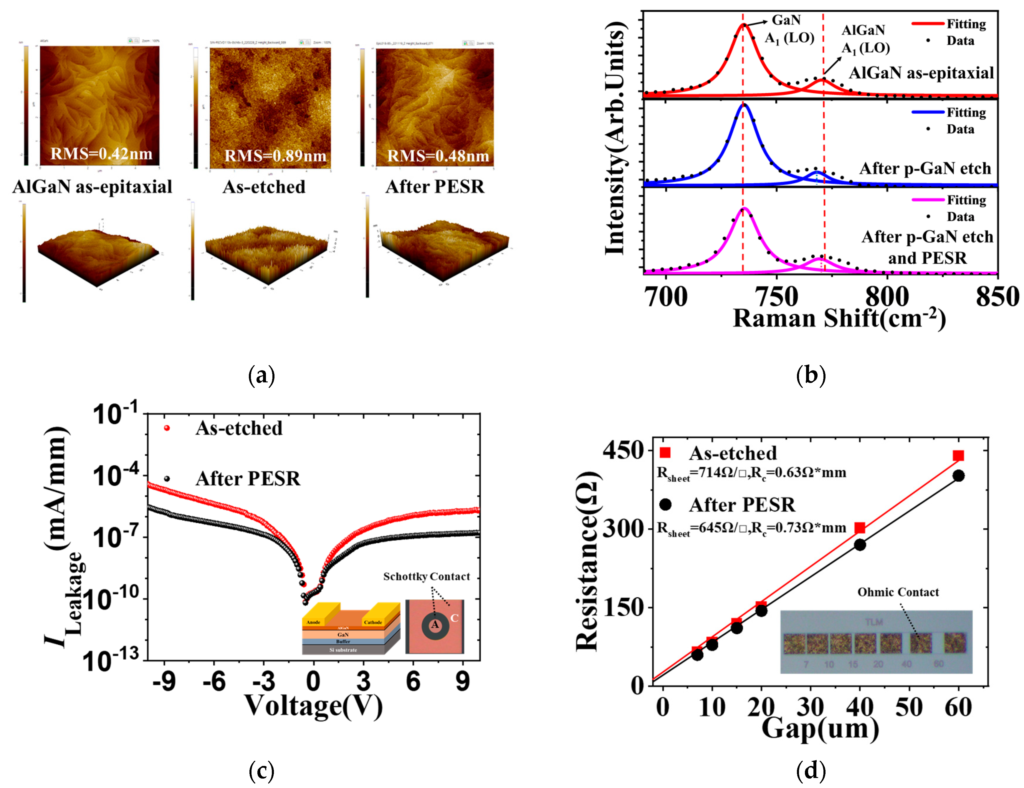
For the as-epitaxial AlGaN surface, the RMS was about 0.42 nm. After p-GaN selective etching, RMS was increased to ~0.89 nm, which was resulted by large numbers of nanopillars on the etched surface as shown in Figure 2a. The developed PESR process could effectively modify the etch-induced damage surface because of the self-limiting properties of O2 plasma oxidation and the following etch step with BCl3 chemistry.
Further surface characterization was performed by Raman under 405 nm excitation laser wavelength at room temperature, as shown in Figure 2b. Compared with the as-grown AlGaN/GaN heterostructure, the AlGaN A1(LO) peak was shifted negatively [16] after p-GaN etch as seen in Figure 2b middle, which indicated near surface lattice damage during the p-GaN etch process. Amazingly as seen in Figure 2b bottom, the AlGaN A1(LO) peak moved back to the as-epitaxial position, which demonstrated the effectiveness of removing the damaged surface with the atomic-level PESR treatment.
Schottky diodes were fabricated on etched AlGaN to characterize the surface quality. As shown in Figure 2c, with the application of PESR technology, the MS Schottky leakage current was reduced by an order of magnitude at 10 V bias. This strongly indicated that the developed PESR process could recover the etched AlGaN surface by self-limiting removing the byproducts or damaged layer after p-GaN etching. Specific contact resistivity (Rc) and sheet resistance measurements (Rsheet) were made using a test pattern conforming to the linear transmission line model (TLM) as described by Reeves et al. [17]. The TLM pattern consists of 100 × 100 μm contact pads with separations of 7 μm, 10 μm, 15 μm, 20 μm, 40 μm, 60 μm. Rsheet and Rc are extracted from the slope and the y-axis intercept of their corresponding linear fits, respectively. As shown in Figure 2d, comparing with as etched sample, the sheet resistance was reduced by 69 Ω/□ after PESR, which indicated that 2DEG transport characteristics was improved.
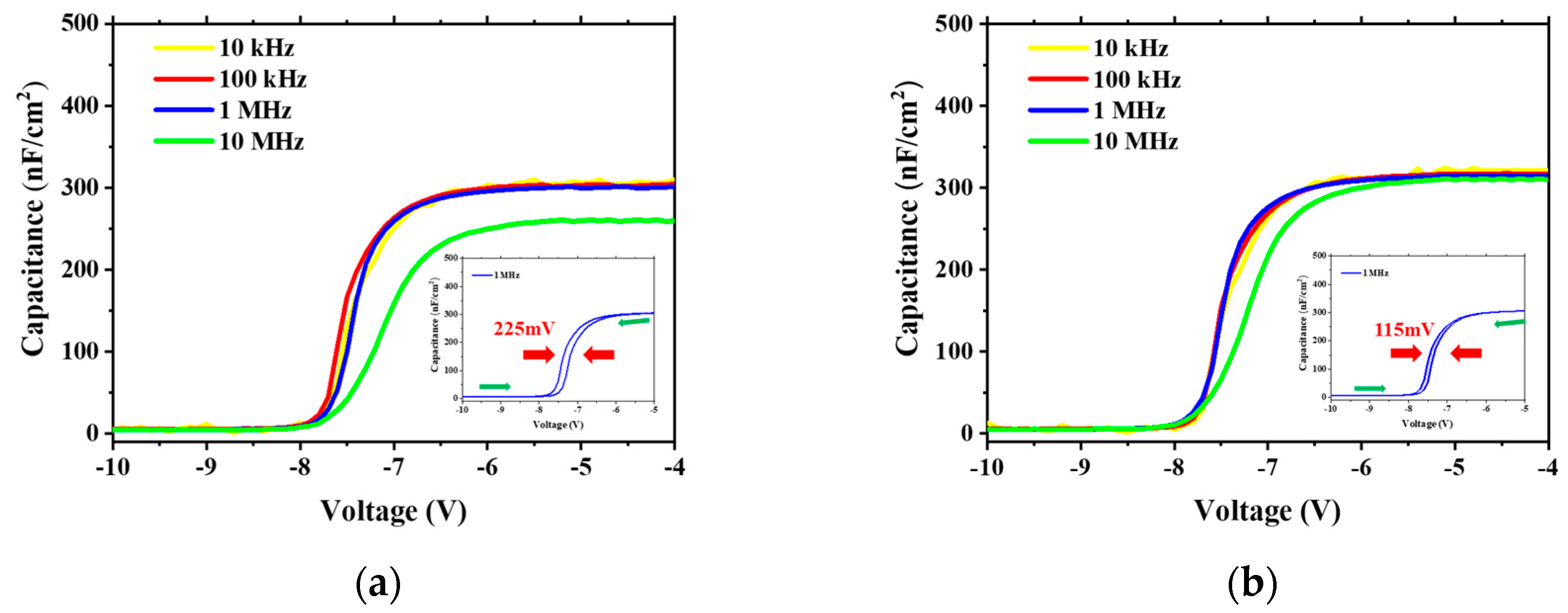
Figure 3a,b show the multi-frequency C-V curves of the TiN/Al2O3/AlGaN/GaN MIS capacitors. The C-V hysteresis at 1 MHz was reduced from ~225 mV to ~115 mV after PESR treatment, indicating that there was less electron trapping in the Al2O3/AlGaN MIS structure. Al2O3/AlGaN interface state density (Dit) was derived from C-V frequency dispersion [18]. For MIS C-V with PESR process, the measured ΔVFB between 100 kHz and 1 MHz was ~180 mV, giving Dit of 7.20 × 1012 cm−2 eV−1 with time constant in the range from 0.16 μs to 1.6 μs. The corresponding Dit for as-etched Al2O3/AlGaN MIS capacitor was as high as 4.62 × 1013 cm−2 eV−1. The decrease of trap states may be attributed to the effect of the beneficial of interface reinforcement. It can be seen that the result in Figure 3b has a less frequency hysteresis and a better high frequency performance.
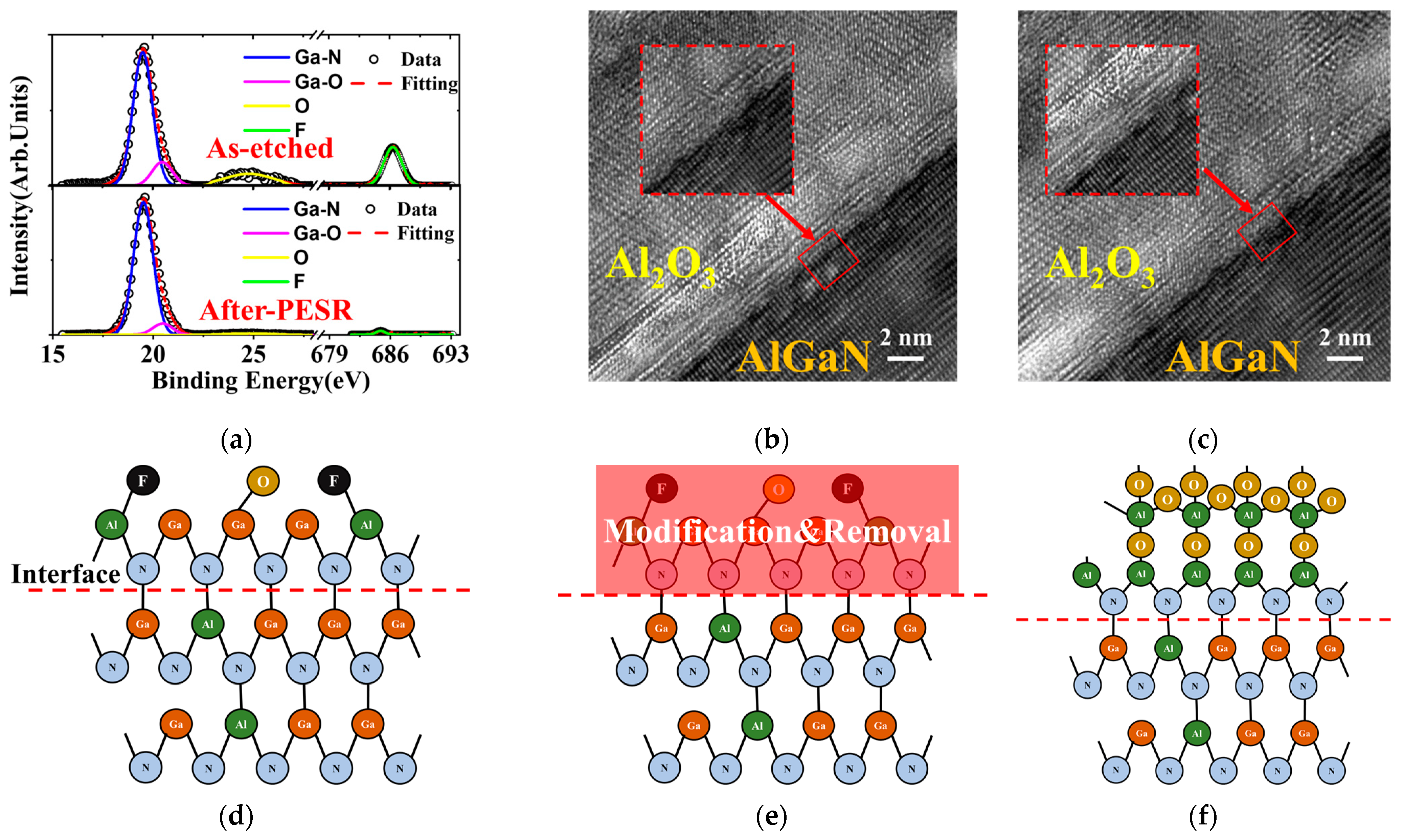
In order to further understand the mechanism of PESR process, both XPS and TEM characterization were performed and analyzed. After normal p-GaN etch, the surface presented a high intensity of F-bond in Figure 4a, indicating a possible amorphous fluoride layer at Al2O3/AlGaN interface. In contrast, the PESR process significantly got rid of the F-bond layer as seen in Figure 4a. Meanwhile, the Ga-O bonds and the native oxides were also effectively suppressed, resulting in a sharper interface between Al2O3 and AlGaN as shown in Figure 4b,c. The whole process was illustrated in the schematic diagram as in Figure 4d–f. The etch-induced byproducts layer was removed and the damaged surface was modified after PESR process, thus generated a better AlGaN surface for later-on ALD-Al2O3 deposition.
Figure 5a shows the p-GaN gate HEMTs transfer characteristics at Vds = 10 V of as-etched and after PESR, respectively. A normally-off operation with a Vth of 1.1 V is achieved. As seen in log-scale, due to the improved Al2O3/AlGaN interface in drift region with PESR process, the device gate leakage Ig was reduced by an order of magnitude, leading to as high as 6 × 10⁹ on-off ratio. The saturated drain current (Isat) of device after PESR is 325 mA/mm at Vg = 5 V, which is about 1.2 times the 270 mA/mm of as-etched one, as illustrated in Figure 5b. The extracted on-resistance (RON) of as-etched device and after PESR one are 14.3 Ω⋅mm and 11.8 Ω⋅mm at Vg = 5 V, respectively.
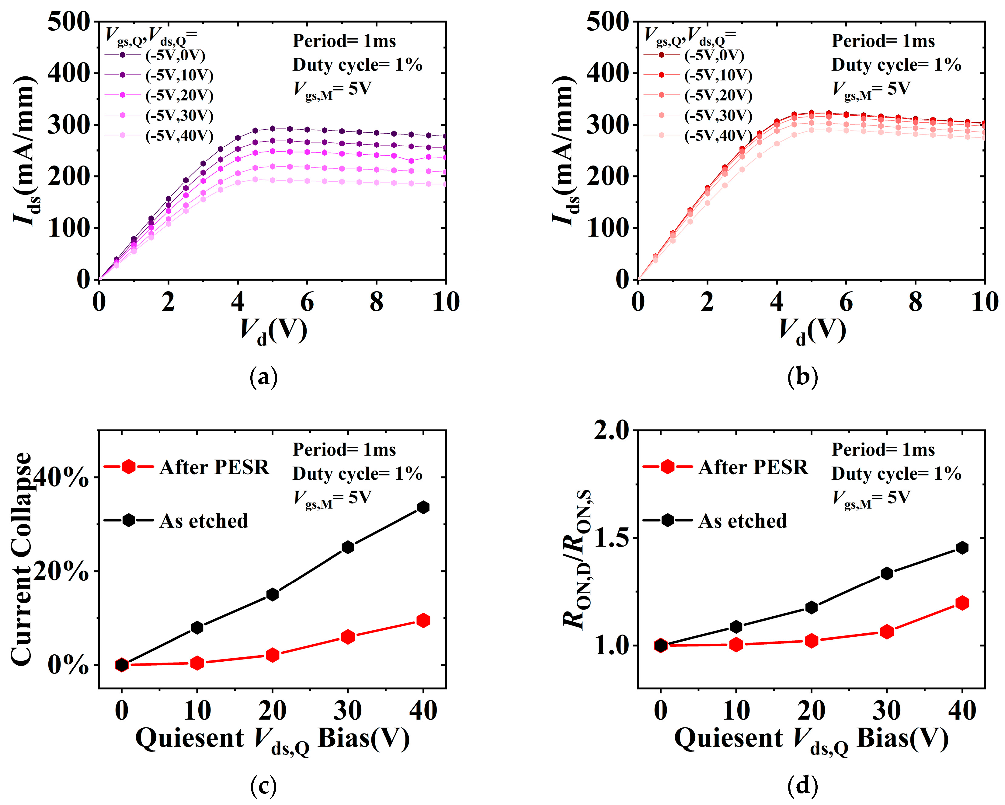
Pulsed Ids-Vds measurements under slow switching were performed to characterize dynamic ON-resistance (RON,D) of the fabricated p-GaN gate HEMTs [19]. The dynamic characteristics of the fabricated p-GaN gate HEMTs were investigated using the Keithley 4200A PMU module with the drain static bias voltage Vds,Q. The period of the square wave pulse signal is 1 ms, the width is 10 μs, the duty cycle is 1%, and the time of pulse rising and falling is set to 500 ns. The device is synchronously switched from an OFF-state quiescent bias of Vgs,Q = −5 V, Vds,Q = 0/10/20/30/40 V to measurement state of Vgs,M = 5 V and Vds from 0 V to 10 V. Figure 6a,b illustrate the current collapse phenomenon under increasing Vds,Q, which was obviously suppressed after PESR process, indicating that Al2O3/AlGaN interface states was improved. Meanwhile, the ratio of RON,D/RON,S for as-etched device was 1.45, which was significantly improved to 1.19 for devices with PESR process at Vgs,Q = 5 V, Vds,Q = 40 V as shown in Figure 6d.

4. Conclusions

In summary, a novel atomic-level post-etch-surface-reinforcement (PESR) process is developed to recover the p-GaN etching induced damage region for high performance p-GaN gate HEMTs fabrication. This process is composed of a surface modification step with O2 plasma, following by an oxide removal step with BCl3 plasma, which made negligible damage on the un-oxidized AlGaN to obtain a high-quality AlGaN surface due to the self-limiting characteristic. As a result, the fabricated HEMTs device performance was significantly enhanced with ~20% lower of on-resistance, and ~25% less of current collapse at Vds,Q bias of 40 V with PESR process, showing great potential of leverage p-GaN gate HEMTs reliability.

Author Contributions

Conceptualization, L.W. and P.Z.; methodology, L.W. and P.Z.; validation, M.X. and C.W. (Chen Wang); formal analysis, L.W., K.Z. and P.Z.; investigation, L.W.; resources, L.W.; data curation, L.W., P.Z., Z.H., K.C., X.S., Y.Y., X.X., H.H. and X.H.; writing—original draft preparation, L.W.; writing—review and editing, P.Z. and M.X.; visualization, Q.W. and M.P.; supervision, C.W. (Chen Wang) and M.X.; project administration, C.W. (Chunlei Wu), C.W. (Chen Wang) and M.X.; funding acquisition, S.X., C.W. (Chen Wang), M.X. and D.W.Z. All authors have read and agreed to the published version of the manuscript.

Funding

This research received no external funding.

Data Availability Statement

Not applicable.

Conflicts of Interest

The authors declare no conflict of interest.

References

  1. Kumazaki, Y.; Uemura, K.; Sato, T.; Hashizume, T. Precise thickness control in recess etching of AlGaN/GaN hetero-structure using photocarrier-regulated electrochemical process. J. Appl. Phys. 2017, 121, 184501. [Google Scholar] [CrossRef]
  2. Millan, J.; Godignon, P.; Perpiñà, X.; Pérez-Tomás, A.; Rebollo, J. A Survey of Wide Bandgap Power Semiconductor Devices. IEEE Trans. Power Electron. 2014, 292, 2155–2163. [Google Scholar] [CrossRef]
  3. Jones, E.A.; Wang, F.F.; Costinett, D. Review of Commercial GaN Power Devices and GaN-Based Converter Design Challenges. IEEE J. Emerg. Sel. Top. Power Electron. 2016, 47, 707–719. [Google Scholar] [CrossRef]
  4. Wang, M.; Chen, K.J. Improvement of the Off-State Breakdown Voltage With Fluorine Ion Implantation in AlGaN/GaN HEMTs. IEEE Trans. Electron Devices 2011, 584, 460–465. [Google Scholar] [CrossRef]
  5. Oka, T.; Nozawa, T. AlGaN/GaN Recessed MIS-Gate HFET With High-Threshold-Voltage Normally-Off Operation for Power Electronics Applications. IEEE Electron Device Lett. 2008, 296, 68–670. [Google Scholar] [CrossRef]
  6. Hu, X.; Simin, G. Enhancement mode AlGaN/GaN HFET with selectively grown pn junction gate. Electron. Lett. 2000, 367, 53–754. [Google Scholar] [CrossRef]
  7. Fujii, T.; Tsuyukuchi, N.; Iwaya, M.; Kamiyama, S.; Amano, H.; Akasaki, I. High On/Off Ratio in Enhancement-Mode AlxGa1-xN/GaN Junction Heterostructure Field-Effect Transistors with P-Type GaN Gate Contact. Jpn. J. Appl. Phys. 2006, 45, L1048. [Google Scholar] [CrossRef]
  8. Uemoto, Y.; Hikita, M.; Ueno, H.; Matsuo, H.; Ishida, H.; Yanagihara, M.; Ueda, T.; Tanaka, T.; Ueda, D. Gate Injection Transistor (GIT)—A Normally-Off AlGaN/GaN Power Transistor Using Conductivity Modulation. IEEE Trans. Electron Devices 2007, 543, 3393–3399. [Google Scholar] [CrossRef]
  9. Ishida, M.; Ueda, T.; Tanaka, T.; Ueda, D. GaN on Si Technologies for Power Switching Devices. IEEE Trans. Electron Devices 2013, 603, 3053–3059. [Google Scholar] [CrossRef]
  10. Marcon, D.; Van Hove, M.; De Jaeger, B.; Posthuma, N.; Wellekens, D.; You, S.; Kang, X.; Wu, T.L.; Willems, M.; Stoffels, S.; et al. Direct comparison of GaN-based e-mode architectures (recessed MISHEMT and p-GaN HEMTs) processed on 200mm GaN-on-Si with Au-free technology. In Proceedings of the Proceedings of SPIE—The International Society for Optical Engineering, San Francisco, CA, USA, 13 March 2015; Volume 9363, Invited paper.
  11. Lükens, G.; Hahn, H.; Kalisch, H.; Vescan, A. Self-Aligned Process for Selectively Etched p-GaN-Gated AlGaN/GaN-on-Si HFETs. IEEE Trans. Electron Devices 2018, 65, 3732–3738. [Google Scholar] [CrossRef]
  12. Su, L.Y.; Lee, F.; Huang, J.J. Enhancement-Mode GaN-Based High-Electron Mobility Transistors on the Si Substrate with a P-Type GaN Cap Layer. IEEE Trans. Electron Devices 2014, 614, 460–465. [Google Scholar] [CrossRef]
  13. Zhang, P.; Wang, L.; Zhu, K.; Yang, Y.; Fan, R.; Pan, M.; Xu, S.; Xu, M.; Wang, C.; Wu, C.; et al. High Selectivity, Low Damage ICP Etching of p-GaN over AlGaN for Normally-off p-GaN HEMTs Application. Micromachines 2022, 13, 589. [Google Scholar] [CrossRef] [PubMed]
  14. Tereshchenko, O.E.; Shaibler, G.E.; Yaroshevich, A.S.; Shevelev, S.V.; Terekhov, A.S.; Lundin, V.V.; Zavarin, E.E.; Besyul’kin, A.I. Low-temperature method of cleaning p-GaN(0001) surfaces for photoemitters with effective negative electron affinity. Phys. Solid State 2004, 46, 1949–1953. [Google Scholar] [CrossRef]
  15. Buttari, D.; Chini, A.; Chakraborty, A.; McCarthy, L.; Xing, H.; Palacios, T.; Shen, L.; Keller, S.; Mishra, U.K. Selective dry etching of GaN over AlGaN in BCl3/SF6 mixtures. Int. J. High Speed Electron. Syst. 2004, 14, 756–761. [Google Scholar] [CrossRef]
  16. Liu, Y.; Chen, D.; Wei, G.; Lin, Z.; He, A.; Li, M.; Wang, P.; Zhang, R.; Zheng, Y. Temperature-dependent ultraviolet Raman scattering and anomalous Raman phenomenon of AlGaN/GaN heterostructure. Opt. Express 2019, 274, 4781–4788. [Google Scholar] [CrossRef] [PubMed]
  17. Reeves, G.K.; Harrison, H.B. Using TLM principles to determine MOSFET contact and parasitic resistance. Solid-State Electron. 1997, 411, 1067–1074. [Google Scholar] [CrossRef]
  18. Ramanan, N.; Lee, B.; Misra, V. Comparison of Methods for Accurate Characterization of Interface Traps in GaN MOS-HFET Devices. IEEE Trans. Electron Devices 2015, 625, 546–553. [Google Scholar] [CrossRef]
  19. Jin, D.; Alamo, J.A.D. Mechanisms responsible for dynamic ON-resistance in GaN high-voltage HEMTs. In Proceedings of the 24th International Symposium on Power Semiconductor Devices and ICs, Bruges, Belgium, 3–7 June 2012. [Google Scholar]
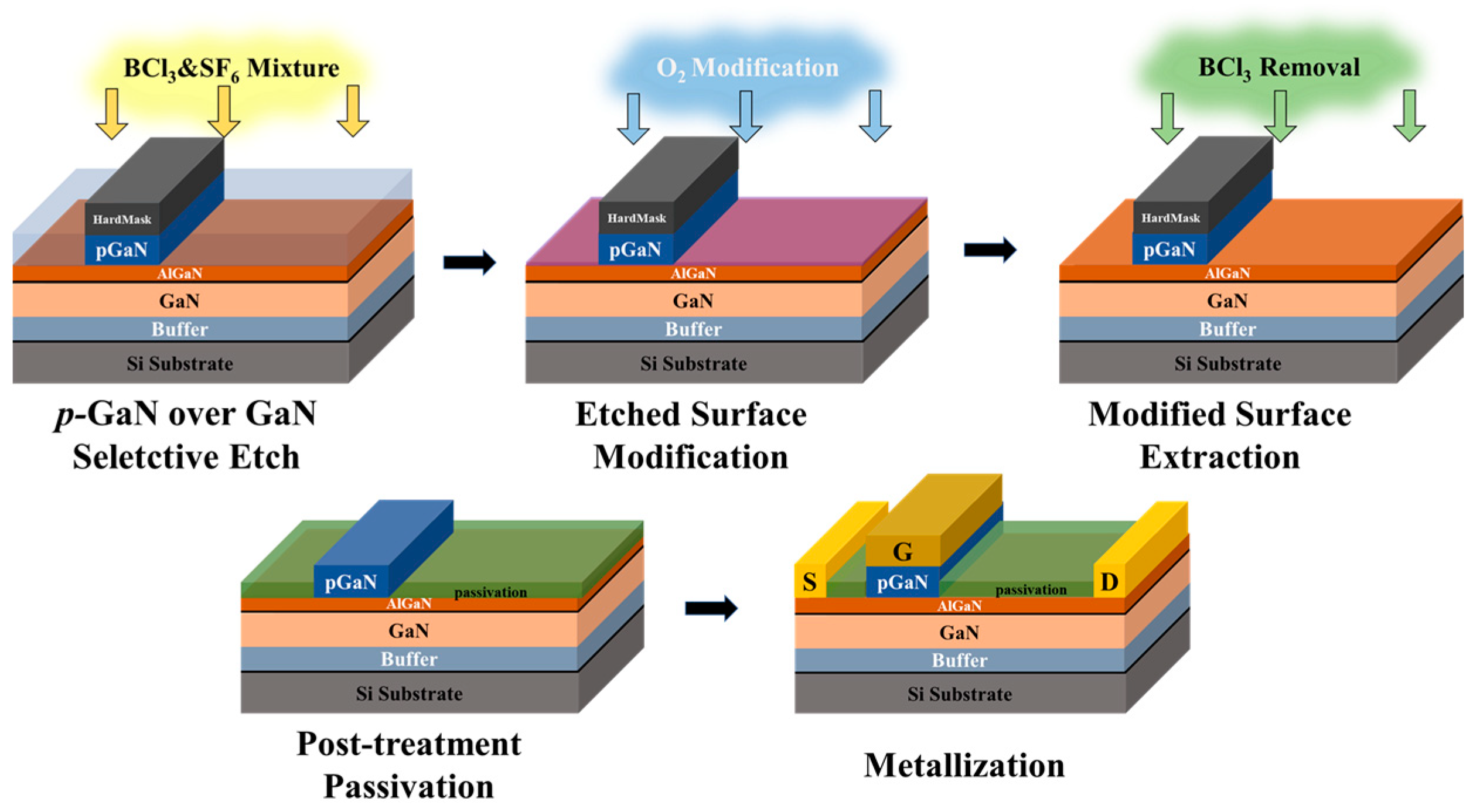
Figure 1. Schematic process flow of the p-GaN gate HEMTs fabrication.
Nanomaterials 13 02275 g001
Figure 2. (a) 5 × 5 μm2 AFM images; (b) The Raman spectra of AlGaN/GaN heterostructure of as-epitaxial AlGaN surface, after p-GaN etch and PESR, after normal p-GaN etch; (c) Leakage current in a Metal-Semiconductor (MS) Schottky Diode; (d) I-V measurements and linear fit for the TLM. The inset shows the TLM patterns.
Nanomaterials 13 02275 g002
Figure 3. Multi-frequency C-V curves for MIS capacitors of (a) after normal p-GaN etch, and (b) after p-GaN etch and with PESR. The insets were the hysteresis curves at 1 MHz.
Nanomaterials 13 02275 g003
Figure 4. XPS spectra of Al2O3/AlGaN interface (a); TEM of Al2O3/AlGaN interface (b) after normal p-GaN etch and (c) after p-GaN etch and PESR; The schematic diagram of atomic level PESR process (df).
Nanomaterials 13 02275 g004
Figure 5. (a) Transfer characteristics in semi-logarithm scale, (b) output characteristics of the fabricated p-GaN gate HEMTs.
Nanomaterials 13 02275 g005
Figure 6. Pulsed Ids-Vds characteristics under different quiescent biases (a) as-etched and (b) after PESR; (c) current collapse and (d) ratio of the dynamic RON,D/RON,S of the fabricated p-GaN gate HEMTs.
Nanomaterials 13 02275 g006
Table 1. The atomic-level PESR process condition.
ParameterO2 ModificationBCl3 Removal
ICP power (W)400200
Bias power (W)06
Chamber pressure (mTorr)1010
Gas flow rate (sccm) 100100
Treatment time (s)155
Disclaimer/Publisher’s Note: The statements, opinions and data contained in all publications are solely those of the individual author(s) and contributor(s) and not of MDPI and/or the editor(s). MDPI and/or the editor(s) disclaim responsibility for any injury to people or property resulting from any ideas, methods, instructions or products referred to in the content.