Article

Probing the Electronic and Opto-Electronic Properties of Multilayer MoS2 Field-Effect Transistors at Low Temperatures

1
School of Physics and Applied Physics, Southern Illinois University, Carbondale, IL 62901, USA
2
Center for Nanophase Materials Sciences, Oak Ridge National Laboratory, Oak Ridge, TN 37830, USA
3
Department of Chemistry, Physics and Atmospheric Science, Jackson State University, Jackson, MS 39217, USA
*
Author to whom correspondence should be addressed.
Nanomaterials 2023, 13(16), 2333; https://doi.org/10.3390/nano13162333
Submission received: 15 June 2023 / Revised: 18 July 2023 / Accepted: 9 August 2023 / Published: 14 August 2023
(This article belongs to the Special Issue Field-Effect Transistors Based on Two-Dimensional Materials)

Abstract

:
Transition metal dichalcogenides (TMDs)-based field-effect transistors (FETs) are being investigated vigorously for their promising applications in optoelectronics. Despite the high optical response reported in the literature, most of them are studied at room temperature. To extend the application of these materials in a photodetector, particularly at a low temperature, detailed understanding of the photo response behavior of these materials at low temperatures is crucial. Here we present a systematic investigation of temperature-dependent electronic and optoelectronic properties of few-layers MoS2 FETs, synthesized using the mechanical exfoliation of bulk MoS2 crystal, on the Si/SiO2 substrate. Our MoS2 FET show a room-temperature field-effect mobility μFE ~40 cm2·V−1·s−1, which increases with decreasing temperature, stabilizing at 80 cm2·V−1·s−1 below 100 K. The temperature-dependent (50 K < T < 300 K) photoconductivity measurements were investigated using a continuous laser source λ = 658 nm (E = 1.88 eV) over a broad range of effective illuminating laser intensity, Peff (0.02 μW < Peff < 0.6 μW). Photoconductivity measurements indicate a fractional power dependence of the steady-state photocurrent. The room-temperature photoresponsivity (R) obtained in these samples was found to be ~2 AW−1, and it increases as a function of decreasing temperature, reaching a maximum at T = 75 K. The optoelectronic properties of MoS2 at a low temperature give an insight into photocurrent generation mechanisms, which will help in altering/improving the performance of TMD-based devices for various applications.

1. Introduction

Owing to the success of synthesis and applications of graphene and graphene-based materials, the scientific community has started to explore the possibility of isolating 2D atomic layers from other layered materials to investigate fundamental physics in non-carbon-based 2D crystals as well as for developing them in future electronic and opto-electronic applications. Recent advances in this area have shown that several other materials, such as hexagonal boron nitride (h-BN), transition metal di-chalcogenides (TMDCs), including MoS2 and WS2, and group III-VI layered semiconductors (e.g., GaSe, InSe, etc.), can be easily exfoliated from bulk crystals or grown using the CVD technique from a single to a few atomic layers [1,2,3,4]. In addition to the 2D structure, these materials also cover a wide range of the spectrum, from the insulator to semiconductors as far as the electrical properties are concerned [4,5,6,7]. For example, hexagonal B-N has a layered structure very similar to graphene, but with a very large band gap [5], whereas TMDs MX2 (M=Mo, W, Re, etc.) have band gap ranges from 0.8 eV to 3 eV and tunable as a function of the number of layers [6]. Some of these crystals, such as MoS2, MoSe2, WS2, WSe2, etc., show indirect to direct band gap transition when they swift from a bulk to single-atomic-layer structure due to the quantum confinement effect [7]. On the other hand, InSe [8,9,10], ReS2 [11], ReSe2 [12] etc., show direct band gap independent to the number of layers. The magnitude of the band gap weakly depends upon the number of layers for ReS2, where single-layer ReS2 shows a gap at 1.5 eV and 1.58 eV for monolayer [11]. Most of the TMDCs have moderate bandgap, which results in a higher ON/OFF current ratio exceeding 107 and small subthreshold voltage swing ~70 mV/decade when exploited as FETs [13]. Apart from FET applications, semiconducting TMDCs also exhibit superior optoelectronic properties, which strongly depend on the number of layers [14]. Additionally, some TMDCs are also strongly correlated electronic materials, exhibiting properties like metal-insulator quantum phase transition, superconductivity, Mott insulator, etc. [15,16,17].
Among the several abovementioned TMDs, the most extensively studied TMD material is MoS2, with thickness ranging from monolayer to several tens of layers [18]. Monolayer MoS2-based FET deices show electronic mobility 200 cm2·V−1·s−1 along with a very high ON/OFF ratio of 108 [13]. Apart from FET applications, numerous studies show strong photo-response properties of 2D-MoS2-based photodetectors with high photo-responsivity and detectivity [19,20]. However, performances of thin MoS2-based photodetectors are mainly limited by low light absorption (5–10%) [20]. Further, most of the past studies are primarily focused on the room temperature as well as low-temperature electronic transport properties of either monolayer or bilayer MoS2-based devices. We have shown in our previous study using indium-selenide-based FET [9] that both the transport mechanism as well as key figures of the merits of an FET device fabricated using a 2D-layered material depends on the number of layers. Additionally, other factors such as surface-induced trap charges, defects inside the MoS2 channel, etc., also result in detrimental photo-response properties, such as short carrier lifetime and persistent photoconductance [21]. In comparison, multilayer MoS2-based devices have several advantageous features, e.g., high density of states resulting in a high drive current as well as tunable electrical properties (n-type and p-type) [22]. However, multilayer MoS2-based FETs and corresponding photo-detection properties have not been extensively studied. In this work, we have fabricated FET devices based on several-layers-thick MoS2 and have systematically studied their electronic and photo-response properties. Multilayer MoS2 FETs show n-type behavior with room-temperature electronic mobility ~40 cm2·V−1·s−1. The electronic mobility increases by almost double ~80 cm2·V−1·s−1 at low temperatures. We further found that maximum photo-responsivity reaches up to ~10 A/W at low temperatures while operating the FETs under the ON condition.

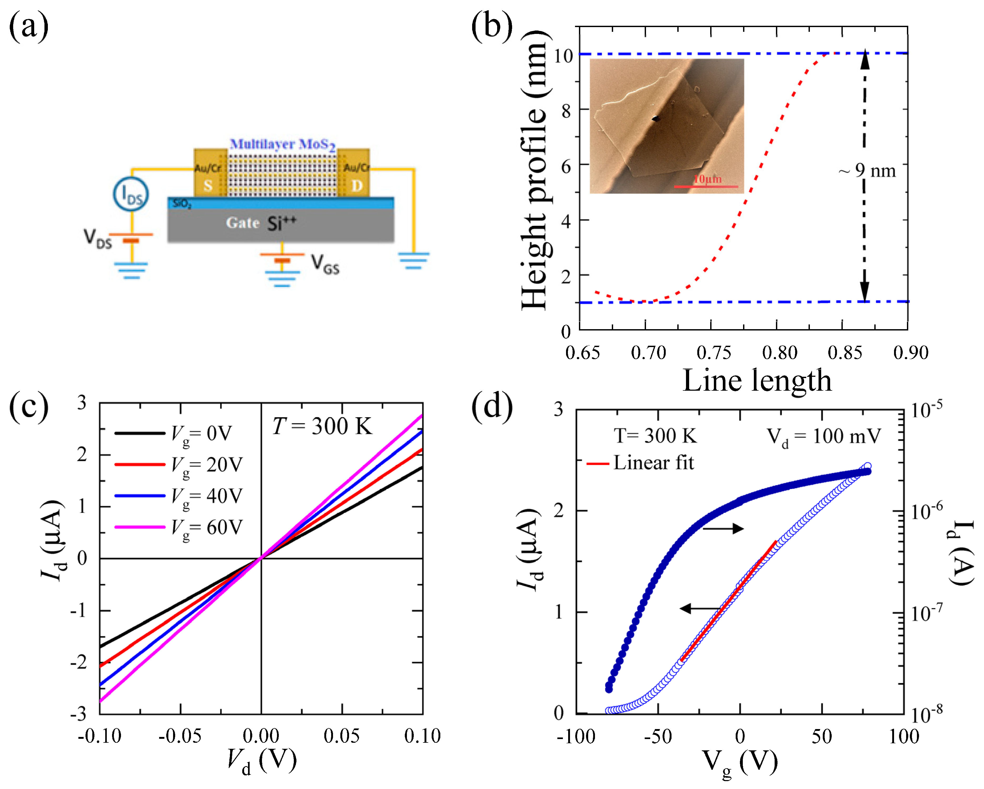
2. Synthesis and Device Fabrication

A few layers of MoS2 were obtained using a mechanical exfoliation technique from commercially available bulk MoS2 crystal (SPI Supplies). The exfoliated flakes/thin layers crystals were subsequently transferred on to a chosen substrate for device fabrication. For device fabrication, we chose a suitable MoS2 flake. Using an optical microscope, a TEM square mesh grid (Electron Microscopy Sciences, Hatfield, PA, USA) was placed carefully on the top of the flake. This mesh grid works as a shadow mask for thermal deposition to put in direct electrical contacts. In this method, we do not use any photoresist or polymers and avoid further fabrication-process-related impurities which may lead to detrimental device performances [23]. After placing this shadow mask, the system was then mounted inside the thermal evaporator. We deposited Cr (10 nm)/Au (100 nm) for the contacts at the chamber pressure 10−6 Torr. The height of the MoS2 flake was measured using atomic force microscopy, ~9–10 nm thick, which corresponds to ~13–15 layers of MoS2. After deposition of the metal electrodes, the devices were annealed at a high temperature in an inert atmosphere.

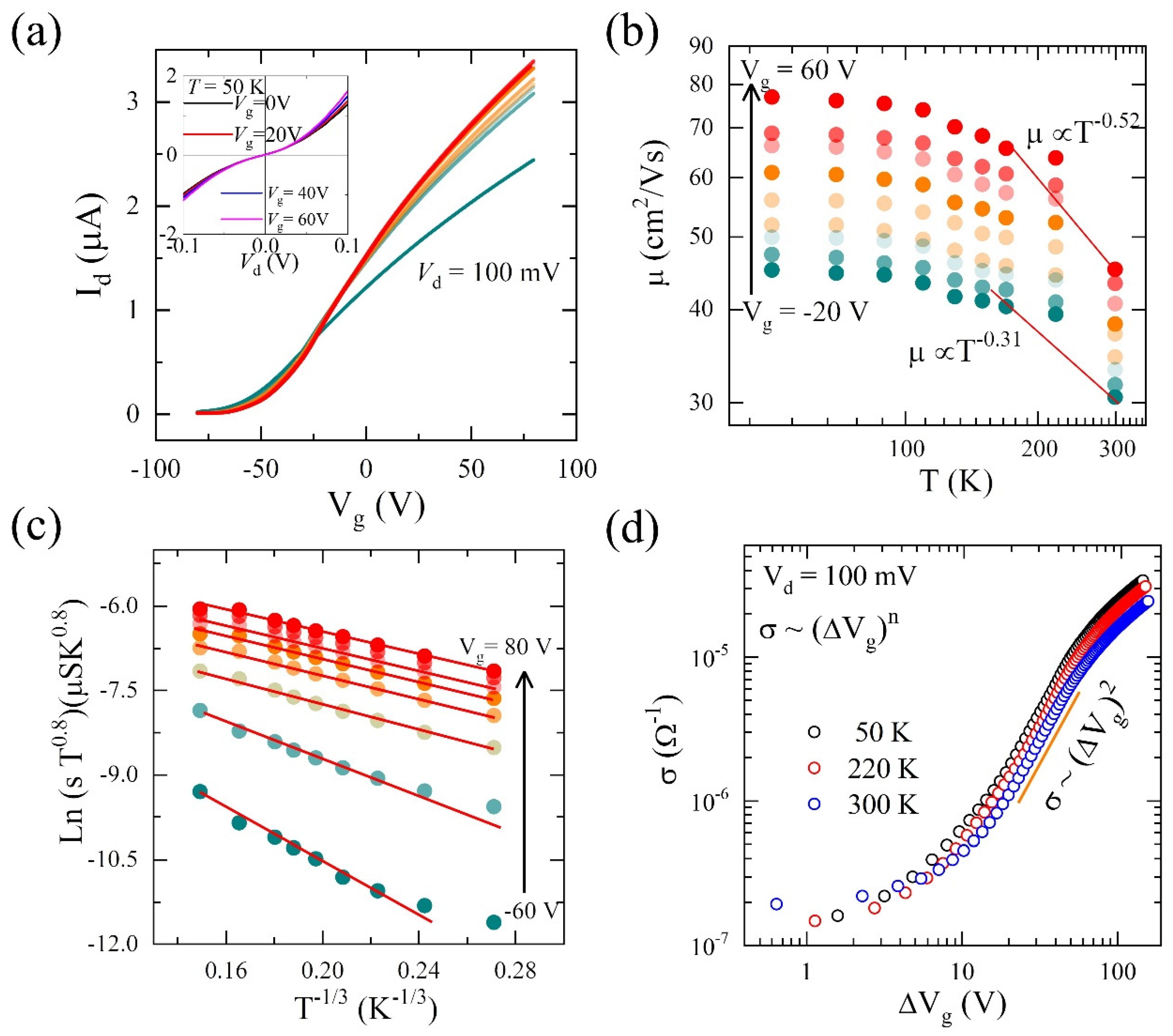
3. Results and Discussion

Three terminal field-effect transistor (FET) measurements were performed on the as prepared MoS2 devices (described in the previous section) under high vacuum ~10−6 Torr and at different sample temperatures 20 K ≤ T ≤ 280 K. To achieve the FET operation, a small d.c voltage (Vd) of 100 mV was applied between the source and drain contacts. The gate voltage was swept between −80 V and +80 V, and the corresponding drain-source currents (Id) were recorded. The fabricated devices were initially used to measure the electrical properties at room temperature. Figure 1a shows the schematic of the device with a laser light illuminating the whole device from the top. Figure 1b shows the optical micrograph image containing the 9–10 nm thick MoS2 device (inset). The channel length and width of the devices is ~10 µm and ~13 µm, respectively.
We used Keithley 2400 SMU to measure the drain-to-source current (Id) by biasing the drain-to-source voltage (Vd), while gate voltages were applied using another Keithley 2410 SMU. The drain-to-source current (Id) as a function of the drain-to-source voltage (Vd) at several gate voltages (Vg) is shown in Figure 1c. The Id-Vd data look linear despite the Schottky barrier between the MoS2 and Cr metal interface due to higher thermionic emission processes at room temperature. The low-temperature Id-Vd data are presented later in this section, which reveal that the metal-semiconductor contacts are indeed of Schottky type. Figure 1d shows the FET transfer characteristics of our MoS2 device at 300 K temperature, showing Id as a function of Vg at Vd = 100 mV. A typical n-type transistor operation was observed with a threshold gate voltage (Vth) ~ −60 V. The drain-source current Id reaches to the maximum saturation value of ~2 μA for gate voltages, Vg > 60 V and remains ~10 nA for Vg < −60 V. From this, we estimated the ON/OFF ratio to be ~102. The low ON/OFF ratio can be attributed to the higher thickness of the MoS2 with a lower bandgap. The red line shows the linear fit of the Id-Vg characteristics plot and was used to extract the field-effect mobility of the device using the MOSFET transconductance formula given below,
μ = L w 1 C d I d d V g 1 V d
where L is the channel length, W is channel width, and C is the capacitance per unit area of the gate dielectric.
This n-type FET operation has been previously observed in many mechanically exfoliated single-layer MoS2 devices. The field-effect electronic mobility was calculated from the linear region by using Equation (1) with an oxide layer thickness of 1000 nm. At 300 K, the field-effect mobility is ~46 cm2·V−1·s−1. This mobility value is similar to the previously obtained room-temperature mobilities of multilayered MoS2 devices [24] and higher than single-layer MoS2 devices [13,15]. However, with appropriate contact engineering, these mobility values can be further improved [25,26,27,28].
This higher mobility is mainly due to the higher density of states and lower Schottky barrier/Ohmic contacts found in the case of our multilayer MoS2 device. Figure 2a shows the low-temperature FET transfer characteristics at different temperatures. We have calculated the back-gated field-effect mobilities at different temperatures, keeping the source-drain voltage constant (100 mV), as shown in Figure 2b. The mobility increases further up to ~80 cm2·V−1·s−1 as the temperature reaches 50 K, which is generally attributed to reduced phonon scattering [29].
The charge carrier transport in 2D semiconductors is mainly dependent on the carrier density or equivalently on the Fermi energy level EF [30,31,32,33]. When the charge carrier density is “very-low”, the Fermi level EF lies in the bandgap region without any mobile carriers. In this case, the system remains in a disorder-driven strongly localized insulating phase. In the case of an n-type semiconductor, the application of a positive gate-bias moves the Fermi level towards the conduction band edge. This results in the generation of mobile electrons by filling up the localized states by thermal excitation. Further increment in the gate bias shifts the Fermi level above the mobility edge, and thus the band transport becomes more dominant. Finally, when the carrier density becomes “very-high”, a strong apparent metallic phase is observed. At higher temperatures and at “very-high” doping level, the charge carrier transport is often influenced by the phonon effects and by short- and long-range scatterers, such as defects and charged impurities. The transition from the insulating state to the conducting state involves gradual progressive filling of the localized states or band edge disordered states arising from impurities and/or structural defects. At the intermediate carrier density level, charge carrier conduction occurs via the hopping of charge carriers through the localized states [34,35,36,37]. These type of conduction mechanisms can be described by the variable range hopping (VRH) model, which can be expressed by the following equation [34,38]:
σ   ( n ,   T ) = A . T m   exp   [ ( T 0 T ) γ ]
where the exponent γ = 1/(d + 1), d is the dimension of the system (d = 1 for 1D system and d = 2 for 2D systems), m = 0.8 is an empirical constant, T is the temperature, T0 is the characteristic temperature, and σ (n, T) is the 2D conductivity.
To further confirm the charge transport mechanism process in our MoS2 devices, we plotted the natural logarithm of the conductance as a function of T−1/3 for different back-gate voltages, as shown in Figure 2c. Here we found that the charge transport for our MoS2 device follows 2D VRH mechanisms, as given by Equation (2), over a wide range of temperatures 50 K ≤ T ≤ 300 K. These 2D VRH mechanisms further support mobility T−1/3 dependence, similar to the results found in monolayer MoS2 devices [34].
In crystalline MoS2, the presence of a high density of localized states in the band-gap region leads to hopping transport when the Femi level moves through them upon changing the gate voltages. According to previous results [34], the physical origin of these localized states in MoS2 films is connected to the random potential fluctuations from the trapped charges at the MoS2-SiO2 interface. Since the screening of these trapped charges is relatively poor due to the large band gap of MoS2, a considerably long band tail thus exists from the interfacial traps which are randomly occupied during the processing of the device. For a 2D system with parabolic energy bands, if the main source of disorder arises from the randomly occupied interfacial traps, the scattering mechanisms are also expected to be dominated by charge impurity scattering [39]. This will further lead to:
σ n   f o r   s c r e e n   c o u l o m b   i m p u r i t y
σ n 2   ( f o r   b a r e   C o u l o m b   i m p u r i t y )
Therefore, to understand the scattering mechanism in our devices, we have plotted the conductance σ as a function of the change in the back-gate voltage (ΔVg) at different temperatures, as shown in Figure 2d. We found that for our MoS2 devices towards the higher gate voltages, σ almost follows the power law expression σ~ΔVg2 for all different temperatures, which indicates scattering from almost unscreened charge impurities in our MoS2 devices.

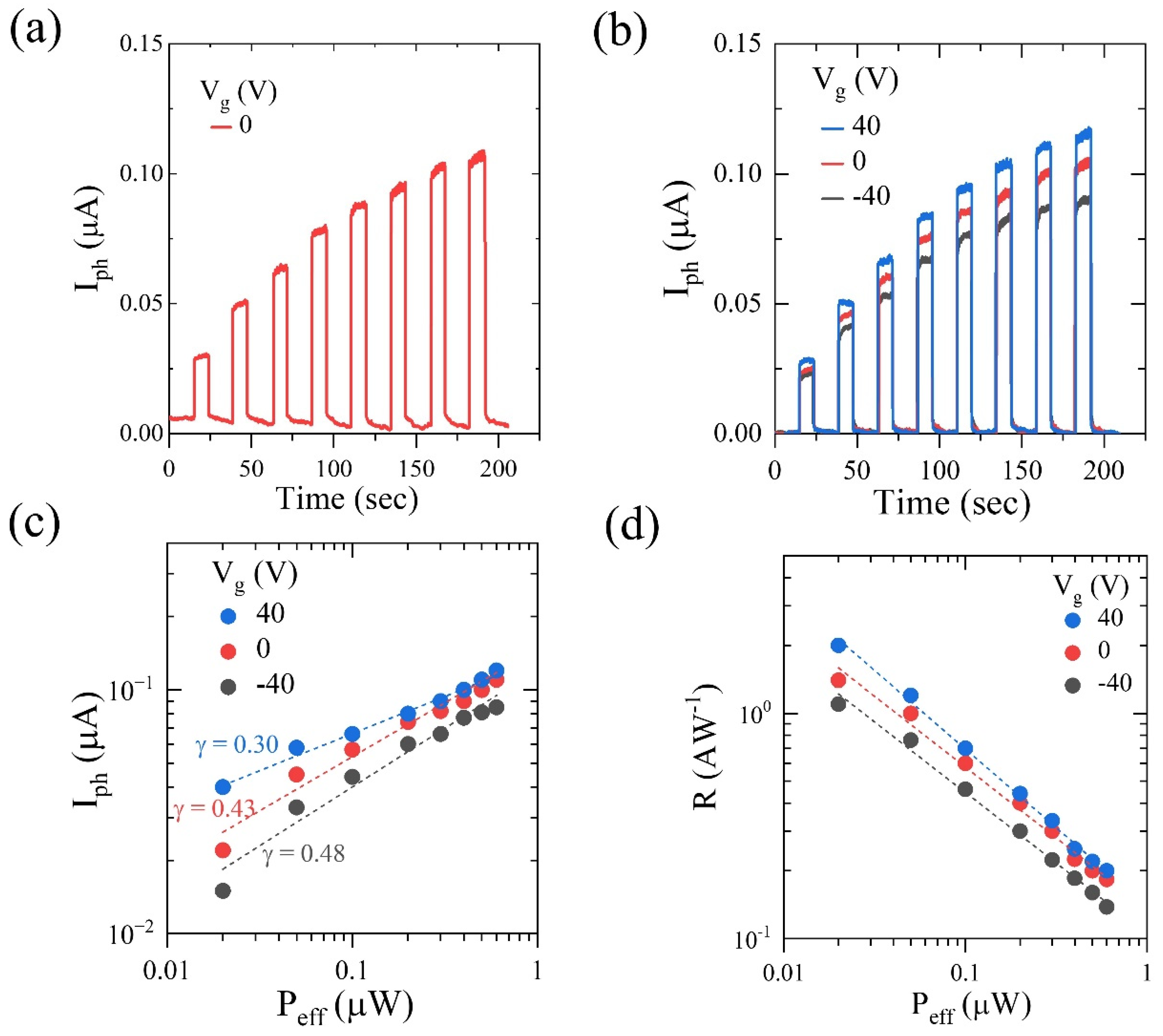
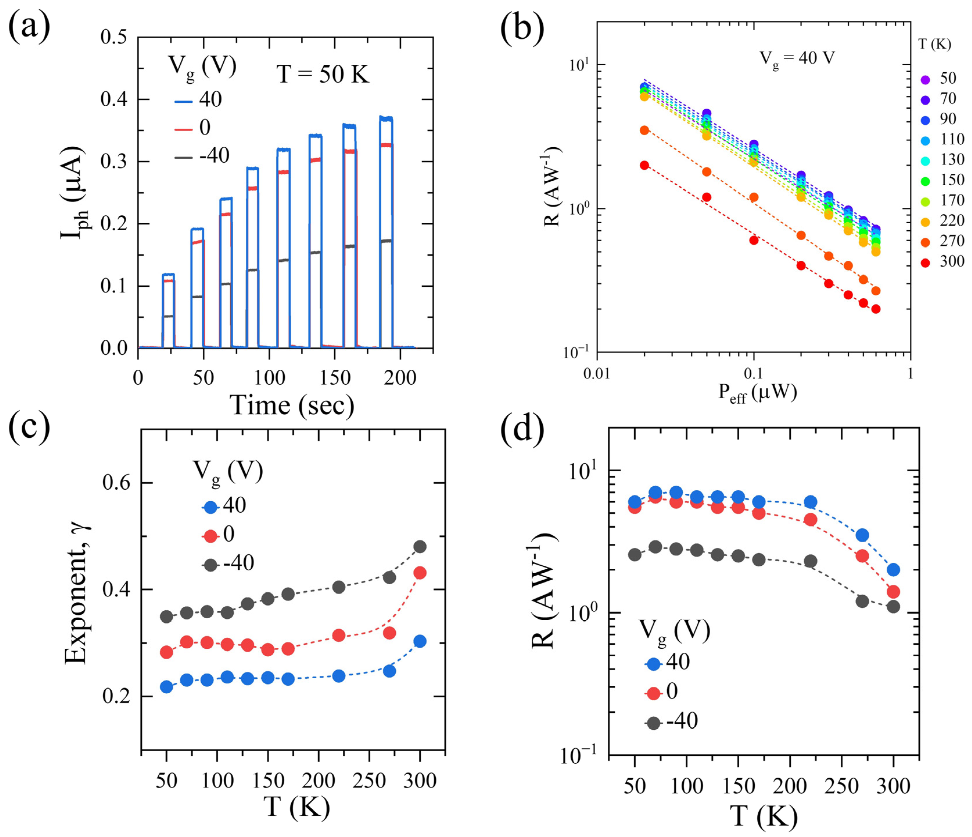
4. Optoelectronic Transport

The optoelectronic properties of MoS2 FET were investigated by using a continuous wave laser with an illumination wavelength λ = 658 nm (E = 1.88 eV) and a spot size of ~3 mm in diameter. A larger laser spot size helps reduces photo-thermal effects, such as the photo-thermoelectric effect, photo-bolometric effect, etc., as both contacts are illuminated alike [40]. Additionally, laser illumination intensity (Plaser) is scaled to an effective laser illumination intensity (Peff) owing to a larger laser spot size as Peff = Plaser × Adevice/Aspot, where Adevice is the area of a device and Aspot is the area of a laser spot. Room-temperature optoelectronic transport measurements of an MoS2 FET are shown in Figure 3. A continuous laser was switched ON and OFF for an interval of ~10 s, and the corresponding drain currents were measured. With the data shown in Figure 3a,b, it can be estimated that the decay response times of this device studied are very fast, perhaps of the order of a few seconds; however, due to the limitation of the measurement system, an accurate determination of this parameter was not possible. Photocurrents (Iph) were estimated as a difference between the drain current under laser illumination (laser on) and the drain current under a dark current (laser off) as Iph = Id,laser ON − Id,laser OFF. The time-dependent response of the photocurrent at Vg = 0 V and various Vg’s is shown in Figure 3a,b, respectively. It was observed that the photocurrent reverts to the drain current under dark conditions as soon as the laser is switched off, implying the presence of only a photoconductive/photogating effect.
The photocurrent (Iph) extracted for three different applied gate voltages (Vg = −40 V, 0 V, 40 V) is plotted as the function Peff in log–log scale, as shown in Figure 3c. The photocurrent follows power law dependence on the effective laser illumination intensity as Iph ∝ (Peff)γ. The value of the exponent is 0 ≤ γ ≤ 1, indicating the presence/absence of trap states in FET. In the absence of trap states, the exponent, γ = 1, and photocurrent generation mechanism follow a pure photoconductive effect. In the presence of trap states, the exponent becomes fractional (γ < 1) and the photocurrent mechanism manifests into a trap-dominated photoconductive effect, commonly known as the photogating effect. It should be noted that crossover of a photo generation mechanism from photoconductive to photogating because of an increased applied gate voltage has been observed in various 2D materials, such as In2Se3 [40], CuIn7Se11 [41], and ReSe2 [42], which indicates that trap states can be modulated. However, the fractional value of γ for all gate voltages (in Figure 3c) indicates that the trap states in MoS2 FET have a strong influence on the optoelectronic properties of MoS2 FETs.
The photo-responsivity (commonly known as responsivity) of a phototransistor can be estimated by R = Iph/Peff. The responsivity as a function of Peff in log–log scale for three different applied gate voltages is shown in Figure 3d. In the case of a pure photoconduction-generated photocurrent (where photoconductive gain is absent), responsivity will have an upper limit, given by R = (η × e × λ)/(h × c) = η × λ/1240, where η is the quantum efficiency, e is the electron charge, h is the plank’s constant, and c is the speed of light [43,44]. For a laser with λ = 658 nm, a maximum R of 0.53 A W−1 can be achieved for η = 1 (100% conversion). For MoS2 FET, responsivity values greater than 0.52 (as seen in Figure 3d) indicate that the gain > 1. Gain can be estimated as τmd, where τm is the minority carrier lifetime and τd is the carrier drift or transit time [45]. For gain > 1, τm > τd, which means that minority carriers are immobile and trapped. This results in a trap-dominated photoconductive effect. As seen in Figure 3d, the responsivity decreases as the effective laser intensity increases, and this could be attributed to a decrease in the average carrier lifetime of minority charge carriers [43]. As light intensity increases, trap states gradually start filling up. At certain light intensities, all the trap states are filled, and a further increase in intensity will result in the generation of minority carriers that cannot be trapped. As a result of this, τm decreases, thus reducing the gain and the responsivity [43]. For MoS2 FET, a maximum R = 2 AW−1 at 300 K can be obtained at Peff = 0.02 μW and Vg = 40 V. When the gain > 1, quantum efficiency (η) is known as the external quantum efficiency (EQE) and is defined as EQE = R (h × c)/(e × λ) = R × 1240/λ. We found a maximum EQE of ~380% at Peff = 0.02 μW and Vg = 40 V.
Temperature plays an important role in determining the strength of traps states. Thus, to emphasize the role of traps states on the photogeneration mechanism, we studied the optoelectronic properties at a low temperature (50 K < T < 300 K). Photocurrents at all studied temperatures show similar behaviors as that of those at room temperature. The time-dependent response of the photocurrent (at various Vg’s) measured at the lowest temperature is shown in Figure 4a, and the photocurrent reverts to the drain current under the dark condition as soon as the laser is switched OFF. Responsivity is a function of Peff at constant Vg = 40 V, and all the temperature studies are shown in Figure 4b. Responsivity increased as temperature decreased, indicating strong trapped states.
The temperature dependence of γ and R is shown in Figure 4c,d, respectively. It is observed that as temperature decreases, gamma decreases, and, correspondingly, responsivity increases for all the studied gate voltages (Vg’s). A strong dependence of γ and R have been observed in various 2D-materials-based FETs, and this was studied in detail in the case of ReSe2 [42]. A clear correlation between R and γ was observed, where lower γ corresponds to higher R. These parameters are determined by trap states, and these traps can be modulated by temperature and gate voltages. In a semiconductor where the steady-state Fermi level is away from the valence band, this results in mid-gap states being available for trapping. Lowering the temperature results in carrier freeze out and strongly trapped minority carriers, resulting in a strong photogating effect. Thus, responsivity increases at lower temperatures.

5. Conclusions

In conclusion, here we have presented the detailed temperature-dependent electronic and optoelectronic properties of few-layers MoS2 FETs. Our MoS2 FETs show mobility μFE ~40 cm2·V−1·s−1 at room temperature and 80 cm2·V−1·s−1 below 100 K. The temperature-dependent (50 K < T < 300 K) photoconductivity measurements show the room-temperature photoresponsivity (R) to be ~2 AW−1, and this increases as a function of decreasing temperature. Photoconductivity measurements indicate a fractional power dependence on the steady-state photocurrent, indicating trap-controlled optoelectronics properties. Understanding the optoelectronic properties of MoS2 at low temperatures will help in altering/improving the performance of TMD-based devices for various applications. Further, these studies may lead to the development of broadband photodetectors, as shown by Wei et al. [46], using ternary-selenide-based materials or components in neuromorphic computing [47].

Author Contributions

Conceptualization, S.G. and S.T.; formal analysis, S.G., J.Z., P.P. and N.P.; funding acquisition, S.T.; investigation, S.G., J.Z. and M.W.; methodology, S.G., J.Z., M.W. and P.P.; project administration, S.T.; resources, S.T.; supervision, S.T.; writing—original draft, P.P.; writing—review and editing, S.G., M.W., P.P., N.P. and S.T. All authors have read and agreed to the published version of the manuscript.

Funding

This work was supported by the U.S. Army Research Office MURI grant #W911NF-11-1-0362. S.T. and P.D.P. acknowledges the support from Indo-U.S. Virtual Networked Joint Center Project on “Light Induced Energy Technologies: Utilizing Promising 2D Nanomaterials (LITE UP 2D)” through the grant number IUSSTF/JC-071/2017. P.D.P. and M.W. acknowledge the support provided by the Southern Illinois University Carbondale, through Graduate School Doctoral Fellowship and College of Science Dissertation Research Award, respectively.

Data Availability Statement

The data that support the findings of this study are available upon request to the authors.

Conflicts of Interest

The authors declare no conflict of interest.

References

  1. Bian, R.; Li, C.; Liu, Q.; Cao, G.; Fu, Q.; Meng, P.; Zhou, J.; Liu, F.; Liu, Z. Recent progress in the synthesis of novel two-dimensional van der Waals materials. Natl. Sci. Rev. 2022, 9, nwab164. [Google Scholar] [CrossRef]
  2. Li, Y.; Kuang, G.; Jiao, Z.; Yao, L.; Duan, R. Recent progress on the mechanical exfoliation of 2D transition metal dichalcogenides. Mater. Res. Express 2022, 9, 122001. [Google Scholar] [CrossRef]
  3. Song, L.; Li, H.; Zhang, Y.; Shi, J. Recent progress of two-dimensional metallic transition metal dichalcogenides: Syntheses, physical properties, and applications. J. Appl. Phys. 2022, 131, 060902. [Google Scholar] [CrossRef]
  4. Lei, Y.; Zhang, T.; Lin, Y.C.; Granzier-Nakajima, T.; Bepete, G.; Kowalczyk, D.A.; Lin, Z.; Zhou, D.; Schranghamer, T.F.; Dodda, A.; et al. Graphene and Beyond: Recent Advances in Two-Dimensional Materials Synthesis, Properties, and Devices. ACS Nanosci. Au 2022, 2, 450–485. [Google Scholar] [CrossRef] [PubMed]
  5. Zhang, K.L.; Feng, Y.L.; Wang, F.; Yang, Z.C.; Wang, J. Two dimensional hexagonal boron nitride (2D-hBN): Synthesis, properties and applications. J. Mater. Chem. C 2017, 5, 11992–12022. [Google Scholar] [CrossRef]
  6. Shanmugam, V.; Mensah, R.A.; Babu, K.; Gawusu, S.; Chanda, A.; Tu, Y.M.; Neisiany, R.E.; Forsth, M.; Sas, G.; Das, O. A Review of the Synthesis, Properties, and Applications of 2D Materials. Part. Part. Syst. Charact. 2022, 39, 2200031. [Google Scholar] [CrossRef]
  7. Chaves, A.; Azadani, J.G.; Alsalman, H.; da Costa, D.R.; Frisenda, R.; Chaves, A.J.; Song, S.H.; Kim, Y.D.; He, D.W.; Zhou, J.D.; et al. Bandgap engineering of two-dimensional semiconductor materials. NPJ 2D Mater. Appl. 2020, 4, 29. [Google Scholar] [CrossRef]
  8. Mudd, G.W.; Molas, M.R.; Chen, X.; Zolyomi, V.; Nogajewski, K.; Kudrynskyi, Z.R.; Kovalyuk, Z.D.; Yusa, G.; Makarovsky, O.; Eaves, L.; et al. The direct-to-indirect band gap crossover in two-dimensional van der Waals Indium Selenide crystals. Sci. Rep. 2016, 6, 39619. [Google Scholar] [CrossRef] [Green Version]
  9. Patil, P.D.; Wasala, M.; Ghosh, S.; Lei, S.D.; Talapatra, S. Broadband photocurrent spectroscopy and temperature dependence of band gap of few-layer indium selenide (InSe). Emergent Mater. 2021, 4, 1029–1036. [Google Scholar] [CrossRef]
  10. Wasala, M.; Patil, P.; Ghosh, S.; Weber, L.; Lei, S.; Talapatra, S. Role of layer thickness and field-effect mobility on photoresponsivity of indium selenide (InSe)-based phototransistors. Oxf. Open Mater. Sci. 2021, 1, itab010. [Google Scholar] [CrossRef]
  11. Gehlmann, M.; Aguilera, I.; Bihlmayer, G.; Nemsak, S.; Nagler, P.; Gospodaric, P.; Zamborlini, G.; Eschbach, M.; Feyer, V.; Kronast, F.; et al. Direct Observation of the Band Gap Transition in Atomically Thin ReS2. Nano Lett. 2017, 17, 5187–5192. [Google Scholar] [CrossRef] [PubMed] [Green Version]
  12. Yang, S.X.; Tongay, S.; Li, Y.; Yue, Q.; Xia, J.B.; Li, S.S.; Li, J.B.; Wei, S.H. Layer-dependent electrical and optoelectronic responses of ReSe2 nanosheet transistors. Nanoscale 2014, 6, 7226–7231. [Google Scholar] [CrossRef] [PubMed]
  13. Radisavljevic, B.; Radenovic, A.; Brivio, J.; Giacometti, V.; Kis, A. Single-layer MoS2 transistors. Nat. Nanotechnol. 2011, 6, 147–150. [Google Scholar] [CrossRef] [PubMed]
  14. Mak, K.F.; Lee, C.; Hone, J.; Shan, J.; Heinz, T.F. Atomically Thin MoS2: A New Direct-Gap Semiconductor. Phys. Rev. Lett. 2010, 105, 136805. [Google Scholar] [CrossRef] [PubMed] [Green Version]
  15. Radisavljevic, B.; Kis, A. Mobility engineering and a metal-insulator transition in monolayer MoS2. Nat. Mater. 2013, 12, 815–820. [Google Scholar] [CrossRef]
  16. Costanzo, D.; Jo, S.; Berger, H.; Morpurgo, A.F. Gate-induced superconductivity in atomically thin MoS2 crystals. Nat. Nanotechnol. 2016, 11, 339–344. [Google Scholar] [CrossRef] [Green Version]
  17. Pradhan, N.R.; McCreary, A.; Rhodes, D.; Lu, Z.G.; Feng, S.M.; Manousakis, E.; Smirnov, D.; Namburu, R.; Dubey, M.; Walker, A.R.H.; et al. Metal to Insulator Quantum-Phase Transition in Few-Layered ReS2. Nano Lett. 2015, 15, 8377–8384. [Google Scholar] [CrossRef] [Green Version]
  18. Wang, H.; Yu, L.L.; Lee, Y.H.; Shi, Y.M.; Hsu, A.; Chin, M.L.; Li, L.J.; Dubey, M.; Kong, J.; Palacios, T. Integrated Circuits Based on Bilayer MoS2 Transistors. Nano Lett. 2012, 12, 4674–4680. [Google Scholar] [CrossRef] [Green Version]
  19. Taffelli, A.; Dire, S.; Quaranta, A.; Pancheri, L. MoS2 Based Photodetectors: A Review. Sensors 2021, 21, 2758. [Google Scholar] [CrossRef]
  20. Nalwa, H.S. A review of molybdenum disulfide (MoS2) based photodetectors: From ultra-broadband, self-powered to flexible devices. RSC Adv. 2020, 10, 30529–30602. [Google Scholar] [CrossRef]
  21. Hu, T.; Zhang, R.; Li, J.-P.; Cao, J.-Y.; Qiu, F. Photodetectors based on two-dimensional MoS2 and its assembled heterostructures. Chip 2022, 1, 100017. [Google Scholar] [CrossRef]
  22. Choi, W.; Cho, M.Y.; Konar, A.; Lee, J.H.; Cha, G.B.; Hong, S.C.; Kim, S.; Kim, J.; Jena, D.; Joo, J.; et al. High-Detectivity Multilayer MoS2 Phototransistors with Spectral Response from Ultraviolet to Infrared. Adv. Mater. 2012, 24, 5832–5836. [Google Scholar] [CrossRef] [PubMed]
  23. Bolshakov, P.; Smyth, C.M.; Khosravi, A.; Zhao, P.; Hurley, P.K.; Hinkle, C.L.; Wallace, R.M.; Young, C.D. Contact Engineering for Dual-Gate MoS2 Transistors Using O2 Plasma Exposure. ACS Appl. Electron. Mater. 2019, 1, 210–219. [Google Scholar] [CrossRef]
  24. Lin, M.-W.; Kravchenko, I.I.; Fowlkes, J.; Li, X.; Puretzky, A.A.; Rouleau, C.M.; Geohegan, D.B.; Xiao, K. Thickness-dependent charge transport in few-layer MoS2 field-effect transistors. Nanotechnology 2016, 27, 165203. [Google Scholar] [CrossRef]
  25. Khan, M.F.; Rehman, S.; Akhtar, I.; Aftab, S.; Ajmal, H.M.S.; Khan, W.; Kim, D.K.; Eom, J. High mobility ReSe2 field effect transistors: Schottky-barrier-height-dependent photoresponsivity and broadband light detection with Co decoration. 2D Materials 2020, 7, 015010. [Google Scholar] [CrossRef]
  26. Smyth, C.M.; Walsh, L.A.; Bolshakov, P.; Catalano, M.; Schmidt, M.; Sheehan, B.; Addou, R.; Wang, L.H.; Kim, J.; Kim, M.J.; et al. Engineering the interface chemistry for scandium electron contacts in WSe2 transistors and diodes. 2D Materials 2019, 6, 045020. [Google Scholar] [CrossRef]
  27. Khan, M.F.; Ahmed, F.; Rehman, S.; Akhtar, I.; Rehman, M.A.; Shinde, P.A.; Khan, K.; Kim, D.K.; Eom, J.; Lipsanen, H.; et al. High performance complementary WS2 devices with hybrid Gr/Ni contacts. Nanoscale 2020, 12, 21280–21290. [Google Scholar] [CrossRef]
  28. Das, S.; Chen, H.Y.; Penumatcha, A.V.; Appenzeller, J. High Performance Multilayer MoS2 Transistors with Scandium Contacts. Nano Lett. 2013, 13, 100–105. [Google Scholar] [CrossRef]
  29. Li, X.F.; Yang, L.M.; Si, M.W.; Li, S.C.; Huang, M.Q.; Ye, P.D.; Wu, Y.Q. Performance Potential and Limit of MoS2 Transistors. Adv. Mater. 2015, 27, 1547–1552. [Google Scholar] [CrossRef]
  30. Abrahams, E.; Kravchenko, S.V.; Sarachik, M.P. Metallic behavior and related phenomena in two dimensions. Rev. Mod. Phys. 2001, 73, 251. [Google Scholar] [CrossRef] [Green Version]
  31. Kravchenko, S.; Sarachik, M. Metal–insulator transition in two-dimensional electron systems. Rep. Prog. Phys. 2003, 67, 1. [Google Scholar] [CrossRef]
  32. Sarma, S.D.; Adam, S.; Hwang, E.; Rossi, E. Electronic transport in two-dimensional graphene. Rev. Mod. Phys. 2011, 83, 407. [Google Scholar] [CrossRef] [Green Version]
  33. Spivak, B.; Kravchenko, S.; Kivelson, S.; Gao, X. Colloquium: Transport in strongly correlated two dimensional electron fluids. Rev. Mod. Phys. 2010, 82, 1743. [Google Scholar] [CrossRef] [Green Version]
  34. Ghatak, S.; Pal, A.N.; Ghosh, A. Nature of electronic states in atomically thin MoS2 field-effect transistors. ACS Nano 2011, 5, 7707–7712. [Google Scholar] [CrossRef] [Green Version]
  35. Jariwala, D.; Sangwan, V.K.; Late, D.J.; Johns, J.E.; Dravid, V.P.; Marks, T.J.; Lauhon, L.J.; Hersam, M.C. Band-like transport in high mobility unencapsulated single-layer MoS2 transistors. Appl. Phys. Lett. 2013, 102, 173107. [Google Scholar] [CrossRef]
  36. Wu, J.; Schmidt, H.; Amara, K.K.; Xu, X.; Eda, G.; Özyilmaz, B. Large thermoelectricity via variable range hopping in chemical vapor deposition grown single-layer MoS2. Nano Lett. 2014, 14, 2730–2734. [Google Scholar] [CrossRef] [PubMed] [Green Version]
  37. Ye, J.; Zhang, Y.; Akashi, R.; Bahramy, M.; Arita, R.; Iwasa, Y. Superconducting dome in a gate-tuned band insulator. Science 2012, 338, 1193–1196. [Google Scholar] [CrossRef]
  38. Mott, N.F.; Davis, E.A. Electronic Processes in Non-Crystalline Materials; OUP Oxford: Oxford, UK, 2012. [Google Scholar]
  39. Adam, S.; Sarma, S.D. Boltzmann transport and residual conductivity in bilayer graphene. Phys. Rev. B 2008, 77, 115436. [Google Scholar] [CrossRef] [Green Version]
  40. Island, J.O.; Blanter, S.I.; Buscema, M.; van der Zant, H.S.J.; Castellanos-Gomez, A. Gate Controlled Photocurrent Generation Mechanisms in High-Gain In2Se3 Phototransistors. Nano Lett. 2015, 15, 7853–7858. [Google Scholar] [CrossRef] [Green Version]
  41. Ghosh, S.; Patil, P.D.; Wasala, M.; Lei, S.D.; Nolander, A.; Sivakumar, P.; Vajtai, R.; Ajayan, P.; Talapatra, S. Fast photoresponse and high detectivity in copper indium selenide (Culn(7)Se(11)) phototransistors. 2D Mater. 2018, 5, 015001. [Google Scholar] [CrossRef]
  42. Patil, P.D.; Wasala, M.; Alkhaldi, R.; Weber, L.; Kovi, K.K.; Chakrabarti, B.; Nash, J.A.; Rhodes, D.; Rosenmann, D.; Divan, R.; et al. Photogating-driven enhanced responsivity in a few-layered ReSe2 phototransistor. J. Mater. Chem. C 2021, 9, 12168–12176. [Google Scholar] [CrossRef]
  43. Fang, H.H.; Hu, W.D. Photogating in Low Dimensional Photodetectors. Adv. Sci. 2017, 4, 1700323. [Google Scholar] [CrossRef] [PubMed]
  44. Zhao, Q.H.; Wang, W.; Carrascoso-Plana, F.; Jie, W.Q.; Wang, T.; Castellanos-Gomez, A.; Frisenda, R. The role of traps in the photocurrent generation mechanism in thin InSe photodetectors. Mater. Horiz. 2020, 7, 252–262. [Google Scholar] [CrossRef] [Green Version]
  45. Buscema, M.; Island, J.O.; Groenendijk, D.J.; Blanter, S.I.; Steele, G.A.; van der Zant, H.S.J.; Castellanos-Gomez, A. Photocurrent generation with two-dimensional van der Waals semiconductors. Chem. Soc. Rev. 2015, 44, 3691–3718. [Google Scholar] [CrossRef] [PubMed] [Green Version]
  46. Wei, Y.; Chen, C.; Tan, C.; He, L.; Ren, Z.; Zhang, C.; Peng, S.; Han, J.; Zhou, H.; Wang, J. High-Performance Visible to Near-Infrared Broadband Bi2O2Se Nanoribbon Photodetectors. Adv. Opt. Mater. 2022, 10, 2201396. [Google Scholar] [CrossRef]
  47. Yang, S.T.; Li, X.Y.; Yu, T.L.; Wang, J.; Fang, H.; Nie, F.; He, B.; Zhao, L.; Lü, W.M.; Yan, S.S.; et al. High-Performance Neuromorphic Computing Based on Ferroelectric Synapses with Excellent Conductance Linearity and Symmetry. Adv. Funct. Mater. 2022, 32, 2202366. [Google Scholar] [CrossRef]
Figure 1. (a) Schematic of the three-terminal device architecture with laser light illumination in the channel region. (b) Height profile of the MoS2 flakes (red dashed line) extracted from the optical image of the device (inset); (c) Id-Vd characteristics of the MoS2 FET device under different back-gate voltages. (d) Transfer (Id-Vg) characteristics of the MoS2 FET in linear scale (left axis) and log scale (right axis). The red color line represents the liner fit.
Nanomaterials 13 02333 g001
Figure 2. (a) Id-Vg characteristics of MoS2 FET at different temperatures (50 K ≤ T ≤ 300 K). (b) Temperature-dependent field-effect electronic mobility under different back-gate voltages. (c) Temperature dependence of conductivity (σ) and variable range hopping (VRH) at different back-gate voltages. (d) Variation in conductivity σ with ΔVg at different temperatures.
Nanomaterials 13 02333 g002
Figure 3. (a) Photocurrent vs. time at room temperature with no back-gate voltage and (b) with different back-gate voltages. (c) Photocurrent vs. effective power illumination in the whole channel region in log–log scale. (d) Responsivity vs. effective power under different back-gate voltages.
Nanomaterials 13 02333 g003
Figure 4. (a) Photocurrent vs. time under different back-gate voltages. (b) Responsivity variation with effective power and temperature under back-gate voltage of 40 V. (c) Exponent (γ) vs. temperature (extracted from (c)); (d) responsivity vs. temperature.
Nanomaterials 13 02333 g004
Disclaimer/Publisher’s Note: The statements, opinions and data contained in all publications are solely those of the individual author(s) and contributor(s) and not of MDPI and/or the editor(s). MDPI and/or the editor(s) disclaim responsibility for any injury to people or property resulting from any ideas, methods, instructions or products referred to in the content.

