
Research Progress in Surface-Enhanced Infrared Absorption Spectroscopy: From Performance Optimization, Sensing Applications, to System Integration


Abstract
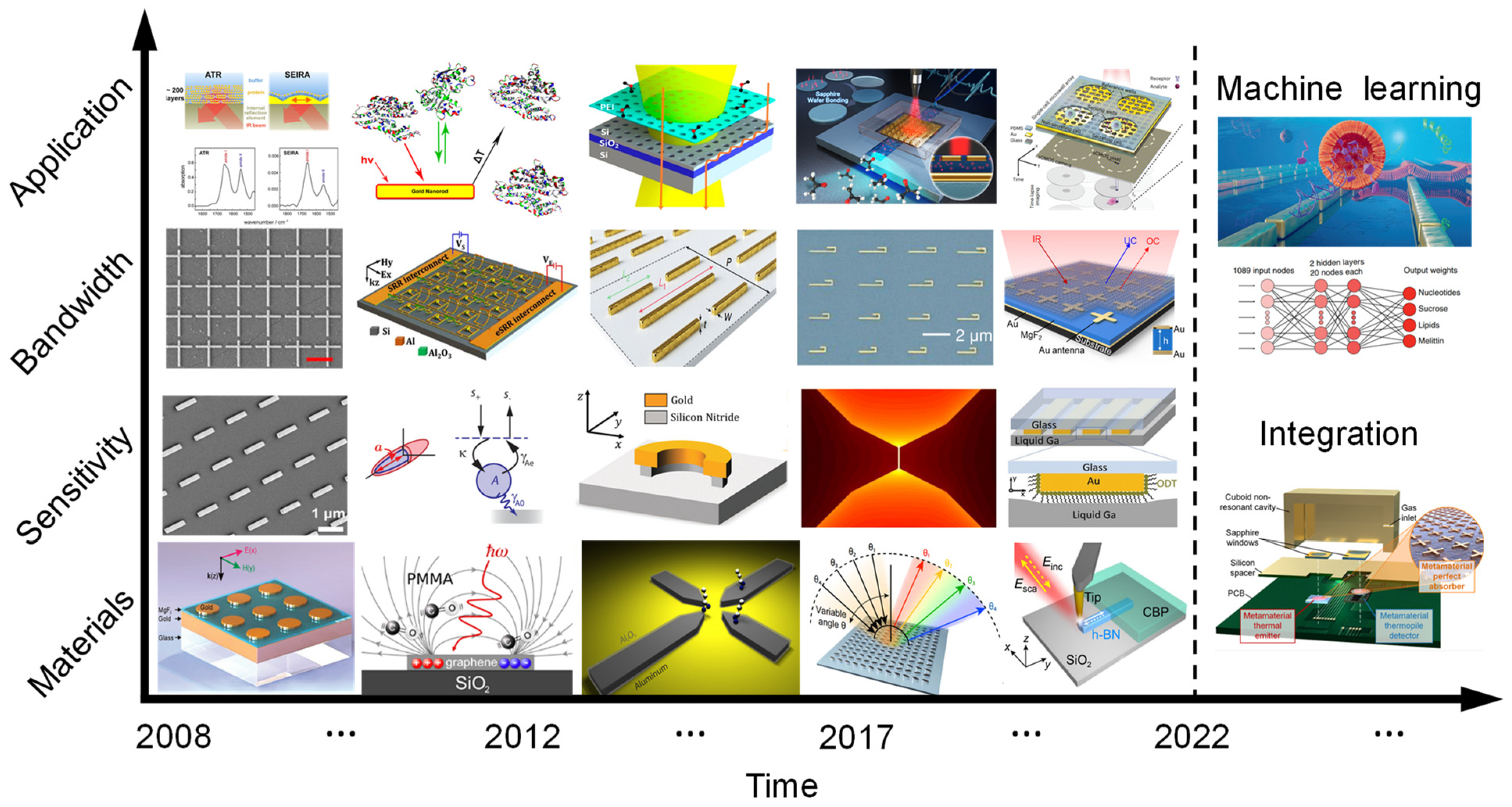
:1. Introduction
2. Resonator Materials
2.1. Metal Materials
2.2. Dielectric Materials
2.3. Phonon Resonance Materials
2.4. Low-Dimensional van der Waals Materials
2.5. Hybrid Materials

3. SEIRA Sensitivity
3.1. Structural Optimization
3.2. Loss Optimization
4. SEIRA Bandwidth
5. Plasmonic Nanostructure-Based Modulating and Sensing Applications
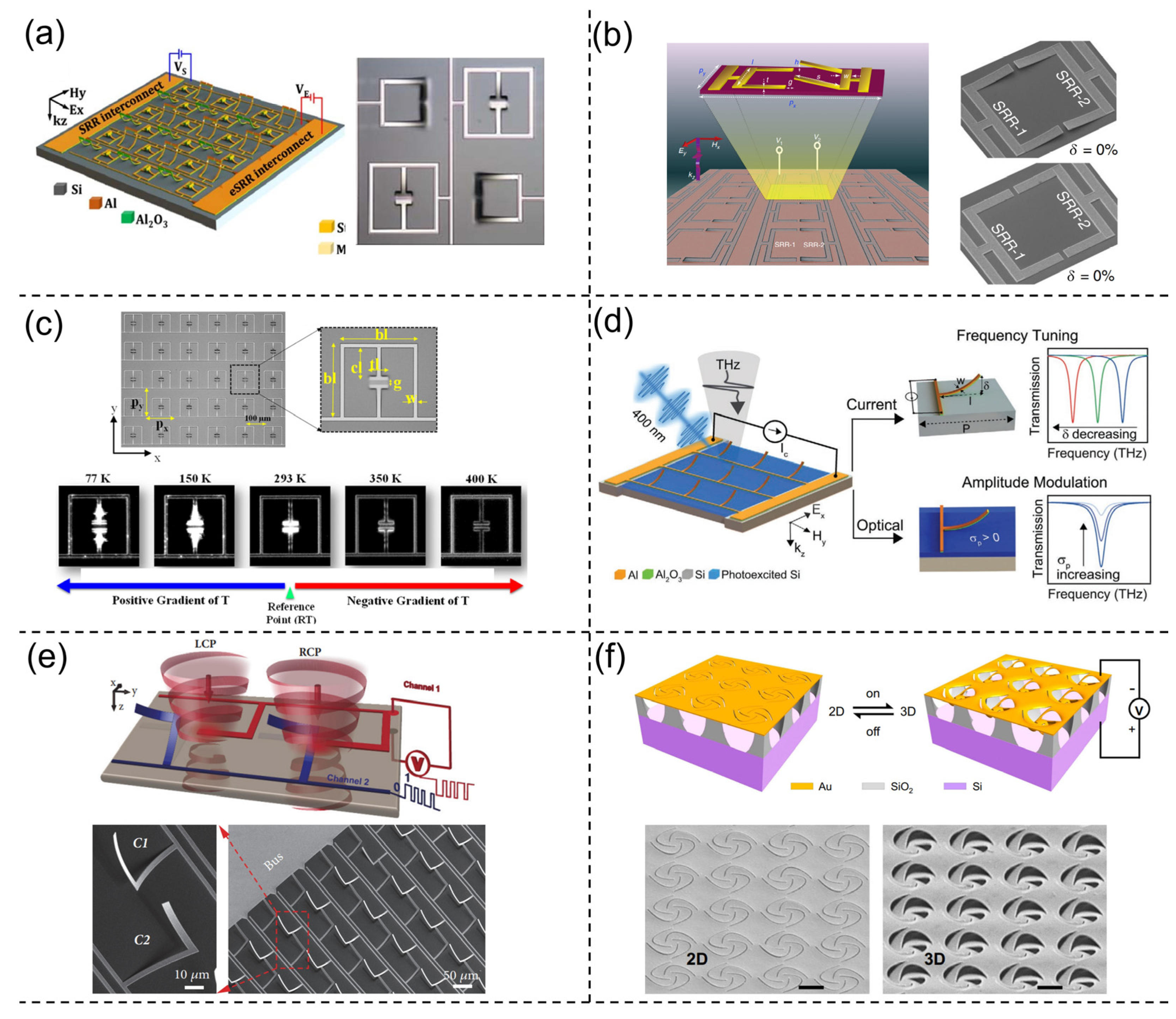
5.1. Mechanical Modulator
5.2. Biomedical and Environmental Sensors
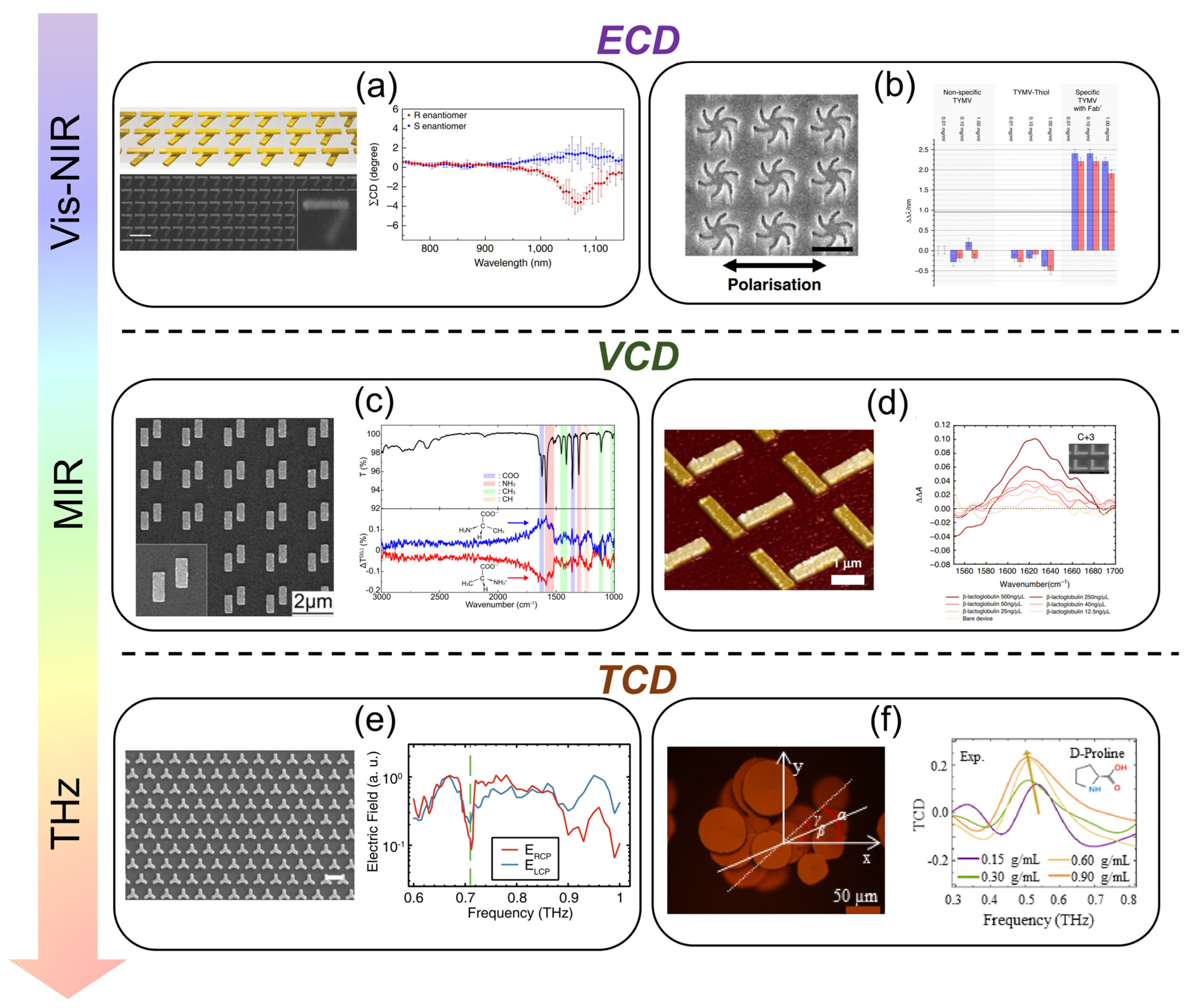
5.3. Chiral Sensor
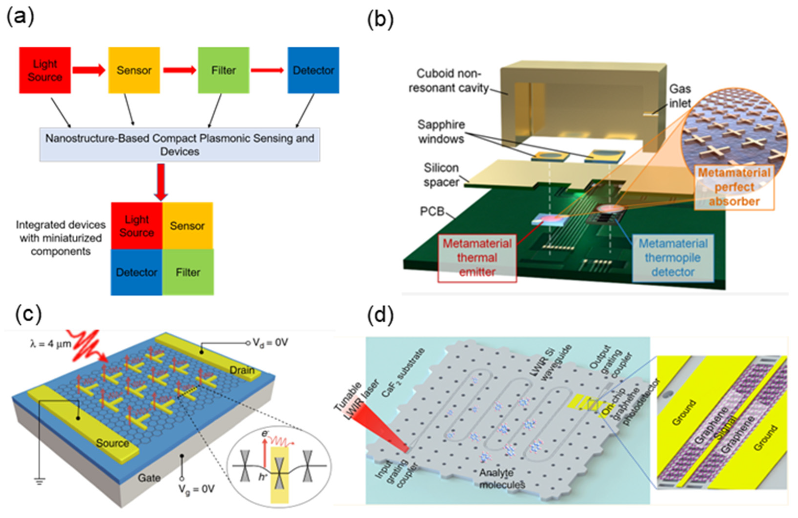
6. System Integration
7. Conclusions
Author Contributions
Funding
Data Availability Statement
Conflicts of Interest
References
- Swinehart, D.F. The Beer-Lambert law. J. Chem. Educ. 1962, 39, 333–335. [Google Scholar] [CrossRef]
- Zhou, H.; Li, D.X.; Hui, X.D.; Mu, X.J. Infrared metamaterial for surface-enhanced infrared absorption spectroscopy: Pushing the frontier of ultrasensitive on-chip sensing. Int. J. Optomechatron. 2021, 15, 97–119. [Google Scholar] [CrossRef]
- Neubrech, F.; Huck, C.; Weber, K.; Pucci, A.; Giessen, H. Surface-Enhanced Infrared Spectroscopy Using Resonant Nanoantennas. Chem. Rev. 2017, 117, 5110–5145. [Google Scholar] [CrossRef] [PubMed]
- Hartstein, A.; Kirtley, J.R.; Tsang, J.C. Enhancement of the Infrared-Absorption from Molecular Monolayers with Thin Metal Overlayers. Phys. Rev. Lett. 1980, 45, 201–204. [Google Scholar] [CrossRef]
- Welford, K. Surface-Plasmon Polaritons and Their Uses. Opt. Quantum Electron. 1991, 23, 1–27. [Google Scholar] [CrossRef]
- Noginov, M.A.; Zhu, G.; Mayy, M.; Ritzo, B.A.; Noginova, N.; Podolskiy, V.A. Stimulated emission of surface plasmon polaritons. Phys. Rev. Lett. 2008, 101, 226806. [Google Scholar] [CrossRef]
- Aroca, R.F.; Ross, D.J.; Domingo, C. Surface-enhanced infrared spectroscopy. Appl. Spectrosc. 2004, 58, 324A–338A. [Google Scholar] [CrossRef]
- Ataka, K.; Heberle, J. Biochemical applications of surface-enhanced infrared absorption spectroscopy. Anal. Bioanal. Chem. 2007, 388, 47–54. [Google Scholar] [CrossRef]
- Kneipp, K.; Wang, Y.; Kneipp, H.; Perelman, L.T.; Itzkan, I.; Dasari, R.; Feld, M.S. Single molecule detection using surface-enhanced Raman scattering (SERS). Phys. Rev. Lett. 1997, 78, 1667–1670. [Google Scholar] [CrossRef]
- Nie, S.M.; Emery, S.R. Probing single molecules and single nanoparticles by surface-enhanced Raman scattering. Science 1997, 275, 1102–1106. [Google Scholar] [CrossRef]
- Zheludev, N.I. The Road Ahead for Metamaterials. Science 2010, 328, 582–583. [Google Scholar] [CrossRef] [PubMed]
- Halas, N.J.; Lal, S.; Chang, W.S.; Link, S.; Nordlander, P. Plasmons in Strongly Coupled Metallic Nanostructures. Chem. Rev. 2011, 111, 3913–3961. [Google Scholar] [CrossRef]
- Brolo, A.G. Plasmonics for future biosensors. Nat. Photonics 2012, 6, 709–713. [Google Scholar] [CrossRef]
- Yang, X.X.; Sun, Z.P.; Low, T.; Hu, H.; Guo, X.D.; de Abajo, F.J.G.; Avouris, P.; Dai, Q. Nanomaterial-Based Plasmon-Enhanced Infrared Spectroscopy. Adv. Mater. 2018, 30, 1704896. [Google Scholar] [CrossRef]
- Yang, K.; Yao, X.; Liu, B.W.; Ren, B. Metallic Plasmonic Array Structures: Principles, Fabrications, Properties, and Applications. Adv. Mater. 2021, 33, 2007988. [Google Scholar] [CrossRef]
- Schuller, J.A.; Barnard, E.S.; Cai, W.; Jun, Y.C.; White, J.S.; Brongersma, M.L. Plasmonics for extreme light concentration and manipulation. Nat. Mater. 2010, 9, 193–204. [Google Scholar] [CrossRef] [PubMed]
- Smith, D.R.; Pendry, J.B.; Wiltshire, M.C.K. Metamaterials and negative refractive index. Science 2004, 305, 788–792. [Google Scholar] [CrossRef]
- Schnell, M.; Garcia-Etxarri, A.; Huber, A.J.; Crozier, K.; Aizpurua, J.; Hillenbrand, R. Controlling the near-field oscillations of loaded plasmonic nanoantennas. Nat. Photonics 2009, 3, 287–291. [Google Scholar] [CrossRef]
- Liu, N.; Langguth, L.; Weiss, T.; Kastel, J.; Fleischhauer, M.; Pfau, T.; Giessen, H. Plasmonic analogue of electromagnetically induced transparency at the Drude damping limit. Nat. Mater. 2009, 8, 758–762. [Google Scholar] [CrossRef]
- Taubert, R.; Hentschel, M.; Kastel, J.; Giessen, H. Classical Analog of Electromagnetically Induced Absorption in Plasmonics. Nano Lett. 2012, 12, 1367–1371. [Google Scholar] [CrossRef]
- Floess, D.; Hentschel, M.; Weiss, T.; Habermeier, H.U.; Jiao, J.; Tikhodeev, S.G.; Giessen, H. Plasmonic Analog of Electromagnetically Induced Absorption Leads to Giant Thin Film Faraday Rotation of 14 degrees. Phys. Rev. X 2017, 7, 021048. [Google Scholar]
- Chen, J.B.; Wang, Y.; Jia, B.H.; Geng, T.; Li, X.P.; Feng, L.; Qian, W.; Liang, B.M.; Zhang, X.X.; Gu, M.; et al. Observation of the inverse Doppler effect in negative-index materials at optical frequencies. Nat. Photonics 2011, 5, 239–242. [Google Scholar] [CrossRef]
- Seddon, N.; Bearpark, T. Observation of the inverse Doppler effect. Science 2003, 302, 1537–1540. [Google Scholar] [CrossRef]
- Parazzoli, C.G.; Greegor, R.B.; Li, K.; Koltenbah, B.E.C.; Tanielian, M. Experimental verification and simulation of negative index of refraction using Snell’s law. Phys. Rev. Lett. 2003, 90, 107401. [Google Scholar] [CrossRef]
- Wang, S.M.; Wu, P.C.; Su, V.C.; Lai, Y.C.; Chen, M.K.; Kuo, H.Y.; Chen, B.H.; Chen, Y.H.; Huang, T.T.; Wang, J.H.; et al. A broadband achromatic metalens in the visible. Nat. Nanotechnol. 2018, 13, 227–232. [Google Scholar] [CrossRef] [PubMed]
- Fan, Z.B.; Qiu, H.Y.; Zhang, H.L.; Pang, X.N.; Zhou, L.D.; Liu, L.; Ren, H.; Wang, Q.H.; Dong, J.W. A broadband achromatic metalens array for integral imaging in the visible. Light Sci. Appl. 2019, 8, 67. [Google Scholar] [CrossRef]
- Baba, T. Slow light in photonic crystals. Nat. Photonics 2008, 2, 465–473. [Google Scholar] [CrossRef]
- Li, G.; Zhang, S.; Zentgraf, T. Nonlinear photonic metasurfaces. Nat. Rev. Mater. 2017, 2, 17010. [Google Scholar] [CrossRef]
- Almeida, E.; Bitton, O.; Prior, Y. Nonlinear metamaterials for holography. Nat. Commun. 2016, 7, 12533. [Google Scholar] [CrossRef]
- Cai, W.S.; Chettiar, U.K.; Kildishev, A.V.; Shalaev, V.M. Optical cloaking with metamaterials. Nat. Photonics 2007, 1, 224–227. [Google Scholar] [CrossRef]
- Sreekanth, K.V.; Alapan, Y.; ElKabbash, M.; Ilker, E.; Hinczewski, M.; Gurkan, U.A.; De Luca, A.; Strangi, G. Extreme sensitivity biosensing platform based on hyperbolic metamaterials. Nat. Mater. 2016, 15, 621–628. [Google Scholar] [CrossRef] [PubMed]
- Wang, W.; Ramezani, M.; Vakevainen, A.I.; Torma, P.; Rivas, J.G.; Odom, T.W. The rich photonic world of plasmonic nanoparticle arrays. Mater. Today 2018, 21, 303–314. [Google Scholar] [CrossRef]
- Altug, H.; Oh, S.H.; Maier, S.A.; Homola, J. Advances and applications of nanophotonic biosensors. Nat. Nanotechnol. 2022, 17, 5–16. [Google Scholar] [CrossRef] [PubMed]
- Leitis, A.; Tseng, M.L.; John-Herpin, A.; Kivshar, Y.S.; Altug, H. Wafer-Scale Functional Metasurfaces for Mid-Infrared Photonics and Biosensing. Adv. Mater. 2021, 33, 2102232. [Google Scholar] [CrossRef] [PubMed]
- Tittl, A.; John-Herpin, A.; Leitis, A.; Arvelo, E.R.; Altug, H. Metasurface-Based Molecular Biosensing Aided by Artificial Intelligence. Angew. Chem. Int. Ed. 2019, 58, 14810–14822. [Google Scholar] [CrossRef] [PubMed]
- Oh, S.H.; Altug, H. Performance metrics and enabling technologies for nanoplasmonic biosensors. Nat. Commun. 2018, 9, 5263. [Google Scholar] [CrossRef]
- Neubrech, F.; Pucci, A.; Cornelius, T.W.; Karim, S.; Garcia-Etxarri, A.; Aizpurua, J. Resonant Plasmonic and Vibrational Coupling in a Tailored Nanoantenna for Infrared Detection. Phys. Rev. Lett. 2008, 101, 157403. [Google Scholar] [CrossRef] [PubMed]
- Adato, R.; Yanik, A.A.; Amsden, J.J.; Kaplan, D.L.; Omenetto, F.G.; Hong, M.K.; Erramilli, S.; Altug, H. Ultra-sensitive vibrational spectroscopy of protein monolayers with plasmonic nanoantenna arrays. Proc. Natl. Acad. Sci. USA 2009, 106, 19227–19232. [Google Scholar] [CrossRef] [PubMed]
- Liu, N.; Mesch, M.; Weiss, T.; Hentschel, M.; Giessen, H. Infrared Perfect Absorber and Its Application as Plasmonic Sensor. Nano Lett. 2010, 10, 2342–2348. [Google Scholar] [CrossRef] [PubMed]
- Chen, K.; Adato, R.; Altug, H. Dual-band perfect absorber for multispectral plasmon-enhanced infrared spectroscopy. ACS Nano 2012, 6, 7998–8006. [Google Scholar] [CrossRef]
- Jiang, X.; Zaitseva, E.; Schmidt, M.; Siebert, F.; Engelhard, M.; Schlesinger, R.; Ataka, K.; Vogel, R.; Heberle, J. Resolving voltage-dependent structural changes of a membrane photoreceptor by surface-enhanced IR difference spectroscopy. Proc. Natl. Acad. Sci. USA 2008, 105, 12113–12117. [Google Scholar] [CrossRef] [PubMed]
- Li, Y.; Yan, H.; Farmer, D.B.; Meng, X.; Zhu, W.; Osgood, R.M.; Heinz, T.F.; Avouris, P. Graphene Plasmon Enhanced Vibrational Sensing of Surface-Adsorbed Layers. Nano Lett. 2014, 14, 1573–1577. [Google Scholar] [CrossRef] [PubMed]
- Adato, R.; Artar, A.; Erramilli, S.; Altug, H. Engineered absorption enhancement and induced transparency in coupled molecular and plasmonic resonator systems. Nano Lett. 2013, 13, 2584–2591. [Google Scholar] [CrossRef]
- Cerjan, B.; Yang, X.; Nordlander, P.; Halas, N.J. Asymmetric Aluminum Antennas for Self-Calibrating Surface Enhanced Infrared Absorption Spectroscopy. ACS Photonics 2016, 3, 354–360. [Google Scholar] [CrossRef]
- Cetin, A.E.; Etezadi, D.; Altug, H. Accessible Nearfields by Nanoantennas on Nanopedestals for Ultrasensitive Vibrational Spectroscopy. Adv. Opt. Mater. 2014, 2, 866–872. [Google Scholar] [CrossRef]
- Pitchappa, P.; Ho, C.P.; Dhakar, L.; Lee, C. Microelectromechanically reconfigurable interpixelated metamaterial for independent tuning of multiple resonances at terahertz spectral region. Optica 2015, 2, 571. [Google Scholar] [CrossRef]
- Rodrigo, D.; Tittl, A.; Ait-Bouziad, N.; John-Herpin, A.; Limaj, O.; Kelly, C.; Yoo, D.; Wittenberg, N.J.; Oh, S.H.; Lashuel, H.A.; et al. Resolving molecule-specific information in dynamic lipid membrane processes with multi-resonant infrared metasurfaces. Nat. Commun. 2018, 9, 2160. [Google Scholar] [CrossRef]
- Mahmoudi, M.; Lohse, S.E.; Murphy, C.J.; Fathizadeh, A.; Montazeri, A.; Suslick, K.S. Variation of protein corona composition of gold nanoparticles following plasmonic heating. Nano Lett. 2014, 14, 6–12. [Google Scholar] [CrossRef]
- Dong, L.; Yang, X.; Zhang, C.; Cerjan, B.; Zhou, L.; Tseng, M.L.; Zhang, Y.; Alabastri, A.; Nordlander, P.; Halas, N.J. Nanogapped Au Antennas for Ultrasensitive Surface-Enhanced Infrared Absorption Spectroscopy. Nano Lett. 2017, 17, 5768–5774. [Google Scholar] [CrossRef]
- Chang, Y.; Hasan, D.; Dong, B.; Wei, J.; Ma, Y.; Zhou, G.; Ang, K.W.; Lee, C. All-Dielectric Surface-Enhanced Infrared Absorption-Based Gas Sensor Using Guided Resonance. ACS Appl. Mater. Interfaces 2018, 10, 38272–38279. [Google Scholar] [CrossRef]
- Leitis, A.; Tittl, A.; Liu, M.; Lee, B.H.; Gu, M.B.; Kivshar, Y.S.; Altug, H. Angle-multiplexed all-dielectric metasurfaces for broadband molecular fingerprint retrieval. Sci. Adv. 2019, 5, eaaw2871. [Google Scholar] [CrossRef] [PubMed]
- Ren, Z.; Zhang, Z.; Wei, J.; Dong, B.; Lee, C. Wavelength-multiplexed hook nanoantennas for machine learning enabled mid-infrared spectroscopy. Nat. Commun. 2022, 13, 3859. [Google Scholar] [CrossRef] [PubMed]
- Xu, J.; Ren, Z.; Dong, B.; Liu, X.; Wang, C.; Tian, Y.; Lee, C. Nanometer-Scale Heterogeneous Interfacial Sapphire Wafer Bonding for Enabling Plasmonic-Enhanced Nanofluidic Mid-Infrared Spectroscopy. ACS Nano 2020, 14, 12159–12172. [Google Scholar] [CrossRef] [PubMed]
- Li, D.; Zhou, H.; Chen, Z.; Ren, Z.; Xu, C.; He, X.; Liu, T.; Chen, X.; Huang, H.; Lee, C.; et al. Ultrasensitive Molecular Fingerprint Retrieval Using Strongly Detuned Overcoupled Plasmonic Nanoantennas. Adv. Mater. 2023, 35, e2301787. [Google Scholar] [CrossRef]
- Miao, X.L.; Luk, T.S.; Liu, P.Q. Liquid-Metal-Based Nanophotonic Structures for High-Performance SEIRA Sensing. Adv. Mater. 2022, 34, e2107950. [Google Scholar] [CrossRef]
- Dolado, I.; Maciel-Escudero, C.; Nikulina, E.; Modin, E.; Calavalle, F.; Chen, S.; Bylinkin, A.; Alfaro-Mozaz, F.J.; Li, J.; Edgar, J.H.; et al. Remote near-field spectroscopy of vibrational strong coupling between organic molecules and phononic nanoresonators. Nat. Commun. 2022, 13, 6850. [Google Scholar] [CrossRef]
- Lochbaum, A.; Dorodnyy, A.; Koch, U.; Koepfli, S.M.; Volk, S.; Fedoryshyn, Y.; Wood, V.; Leuthold, J. Compact Mid-Infrared Gas Sensing Enabled by an All-Metamaterial Design. Nano Lett. 2020, 20, 4169–4176. [Google Scholar] [CrossRef]
- Ansaryan, S.; Liu, Y.C.; Li, X.; Economou, A.M.; Eberhardt, C.S.; Jandus, C.; Altug, H. High-throughput spatiotemporal monitoring of single-cell secretions via plasmonic microwell arrays. Nat. Biomed. Eng. 2023, 7, 943–958. [Google Scholar] [CrossRef]
- Zheng, J.; Cheng, X.; Zhang, H.; Bai, X.; Ai, R.; Shao, L.; Wang, J. Gold Nanorods: The Most Versatile Plasmonic Nanoparticles. Chem. Rev. 2021, 121, 13342–13453. [Google Scholar] [CrossRef]
- John-Herpin, A. Metasurface-Enhanced Infrared Spectroscopy: An Abundance of Materials and Functionalities. Adv. Mater. 2022, e2110163. [Google Scholar] [CrossRef]
- Adato, R.; Altug, H. In-situ ultra-sensitive infrared absorption spectroscopy of biomolecule interactions in real time with plasmonic nanoantennas. Nat. Commun. 2013, 4, 2154. [Google Scholar] [CrossRef]
- Hui, X.; Yang, C.; Li, D.; He, X.; Huang, H.; Zhou, H.; Chen, M.; Lee, C.; Mu, X. Infrared Plasmonic Biosensor with Tetrahedral DNA Nanostructure as Carriers for Label-Free and Ultrasensitive Detection of miR-155. Adv. Sci. 2021, 8, e2100583. [Google Scholar] [CrossRef] [PubMed]
- John-Herpin, A.; Kavungal, D.; von Mucke, L.; Altug, H. Infrared Metasurface Augmented by Deep Learning for Monitoring Dynamics between All Major Classes of Biomolecules. Adv. Mater. 2021, 33, e2006054. [Google Scholar] [CrossRef] [PubMed]
- Kim, J.Y.; Kim, H.; Kim, B.H.; Chang, T.; Lim, J.; Jin, H.M.; Mun, J.H.; Choi, Y.J.; Chung, K.; Shin, J.; et al. Highly tunable refractive index visible-light metasurface from block copolymer self-assembly. Nat. Commun. 2016, 7, 12911. [Google Scholar] [CrossRef] [PubMed]
- Zhou, H.; Yang, C.; Hu, D.; Li, D.; Hui, X.; Zhang, F.; Chen, M.; Mu, X. Terahertz biosensing based on bi-layer metamaterial absorbers toward ultra-high sensitivity and simple fabrication. Appl. Phys. Lett. 2019, 115, 143507. [Google Scholar] [CrossRef]
- Zhou, H.; Hu, D.; Yang, C.; Chen, C.; Ji, J.; Chen, M.; Chen, Y.; Yang, Y.; Mu, X. Multi-Band Sensing for Dielectric Property of Chemicals Using Metamaterial Integrated Microfluidic Sensor. Sci. Rep. 2018, 8, 14801. [Google Scholar] [CrossRef]
- Liu, X.Y.; Liu, W.D.; Yang, B. Deep-elliptical-silver-nanowell arrays (d-EAgNWAs) fabricated by stretchable imprinting combining colloidal lithography: A highly sensitive plasmonic sensing platform. Nano Res. 2019, 12, 845–853. [Google Scholar] [CrossRef]
- Zhuo, X.L.; Yip, H.K.; Ruan, Q.F.; Zhang, T.K.; Zhu, X.Z.; Wang, J.F.; Lin, H.Q.; Xu, J.B.; Yang, Z. Broadside Nanoantennas Made of Single Silver Nanorods. ACS Nano 2018, 12, 1720–1731. [Google Scholar] [CrossRef]
- Li, N.N.; Yin, H.; Zhuo, X.L.; Yang, B.C.; Zhu, X.M.; Wang, J.F. Infrared-Responsive Colloidal Silver Nanorods for Surface-Enhanced Infrared Absorption. Adv. Opt. Mater. 2018, 6, 1800436. [Google Scholar] [CrossRef]
- Jin, D.F.; Hu, Q.; Neuhauser, D.; von Cube, F.; Yang, Y.Y.; Sachan, R.; Luk, T.S.; Bell, D.C.; Fang, N.X. Quantum-Spillover-Enhanced Surface-Plasmonic Absorption at the Interface of Silver and High-Index Dielectrics. Phys. Rev. Lett. 2015, 115, 193901. [Google Scholar] [CrossRef]
- Bohme, A.; Sterl, F.; Kath, E.; Ubl, M.; Manninen, V.; Giessen, H. Electrochemistry on Inverse Copper Nanoantennas: Active Plasmonic Devices with Extraordinarily Large Resonance Shift. ACS Photonics 2019, 6, 1863–1868. [Google Scholar] [CrossRef]
- Tzschoppe, M.; Huck, C.; Vogt, J.; Neubrech, F.; Pucci, A. Impact of Metal-Optical Properties on Surface-Enhanced Infrared Absorption. J. Phys. Chem. C 2018, 122, 15678–15687. [Google Scholar] [CrossRef]
- Liu, Z.; Liu, G.; Liu, X.; Wang, Y.; Fu, G. Titanium resonators based ultra-broadband perfect light absorber. Opt. Mater. 2018, 83, 118–123. [Google Scholar] [CrossRef]
- Zhou, Y.; Qin, Z.; Liang, Z.; Meng, D.; Xu, H.; Smith, D.R.; Liu, Y. Ultra-broadband metamaterial absorbers from long to very long infrared regime. Light Sci. Appl. 2021, 10, 138. [Google Scholar] [CrossRef] [PubMed]
- Herkert, E.; Sterl, F.; Strohfeldt, N.; Walter, R.; Giessen, H. Low-Cost Hydrogen Sensor in the ppm Range with Purely Optical Readout. ACS Sens. 2020, 5, 978–983. [Google Scholar] [CrossRef]
- Duan, X.Y.; Kamin, S.; Sterl, F.; Giessen, H.; Liu, N. Hydrogen-Regulated Chiral Nanoplasmonics. Nano Lett. 2016, 16, 1462–1466. [Google Scholar] [CrossRef]
- Tittl, A.; Mai, P.; Taubert, R.; Dregely, D.; Liu, N.; Giessen, H. Palladium-Based Plasmonic Perfect Absorber in the Visible Wavelength Range and Its Application to Hydrogen Sensing. Nano Lett. 2011, 11, 4366–4369. [Google Scholar] [CrossRef]
- Liu, N.; Tang, M.L.; Hentschel, M.; Giessen, H.; Alivisatos, A.P. Nanoantenna-enhanced gas sensing in a single tailored nanofocus. Nat. Mater. 2011, 10, 631–636. [Google Scholar] [CrossRef]
- Najem, M.; Carcenac, F.; Taliercio, T.; Gonzalez-Posada, F. Aluminum Bowties for Plasmonic-Enhanced Infrared Sensing. Adv. Opt. Mater. 2022, 10, 2201025. [Google Scholar] [CrossRef]
- Su, M.-N.; Dongare, P.D.; Chakraborty, D.; Zhang, Y.; Yi, C.; Wen, F.; Chang, W.-S.; Nordlander, P.; Sader, J.E.; Halas, N.J.; et al. Optomechanics of Single Aluminum Nanodisks. Nano Lett. 2017, 17, 2575–2583. [Google Scholar] [CrossRef]
- Zhou, L.; Zhang, C.; McClain, M.J.; Manavacas, A.; Krauter, C.M.; Tian, S.; Berg, F.; Everitt, H.O.; Carter, E.A.; Nordlander, P.; et al. Aluminum Nanocrystals as a Plasmonic Photocatalyst for Hydrogen Dissociation. Nano Lett. 2016, 16, 1478–1484. [Google Scholar] [CrossRef]
- Chen, K.; Thang Duy, D.; Ishii, S.; Aono, M.; Nagao, T. Infrared Aluminum Metamaterial Perfect Absorbers for Plasmon-Enhanced Infrared Spectroscopy. Adv. Funct. Mater. 2015, 25, 6637–6643. [Google Scholar] [CrossRef]
- Martin, J.; Plain, J. Fabrication of aluminium nanostructures for plasmonics. J. Phys. D-Appl. Phys. 2015, 48, 184002. [Google Scholar] [CrossRef]
- Canalejas-Tejero, V.; Herranz, S.; Bellingham, A.; Moreno-Bondi, M.C.; Barrios, C.A. Passivated aluminum nanohole arrays for label-free biosensing applications. ACS Appl. Mater. Interfaces 2014, 6, 1005–1010. [Google Scholar] [CrossRef]
- Tittl, A.; Leitis, A.; Liu, M.; Yesilkoy, F.; Choi, D.Y.; Neshev, D.N.; Kivshar, Y.S.; Altug, H. Imaging-based molecular barcoding with pixelated dielectric metasurfaces. Science 2018, 360, 1105–1109. [Google Scholar] [CrossRef] [PubMed]
- Bontempi, N.; Chong, K.E.; Orton, H.W.; Staude, I.; Choi, D.-Y.; Alessandri, I.; Kivshar, Y.S.; Neshev, D.N. Highly sensitive biosensors based on all-dielectric nanoresonators. Nanoscale 2017, 9, 4972–4980. [Google Scholar] [CrossRef]
- Hogan, N.J.; Urban, A.S.; Ayala-Orozco, C.; Pimpinelli, A.; Nordlander, P.; Halas, N.J. Nanoparticles heat through light localization. Nano Lett. 2014, 14, 4640–4645. [Google Scholar] [CrossRef]
- Kuznetsov, A.I.; Miroshnichenko, A.E.; Brongersma, M.L.; Kivshar, Y.S.; Luk’yanchuk, B. Optically resonant dielectric nanostructures. Science 2016, 354, aag2472. [Google Scholar] [CrossRef]
- Decker, M.; Staude, I. Resonant dielectric nanostructures: A low-loss platform for functional nanophotonics. J. Opt. 2016, 18, 103001. [Google Scholar] [CrossRef]
- Zheludev, N.I.; Kivshar, Y.S. From metamaterials to metadevices. Nat. Mater. 2012, 11, 917–924. [Google Scholar] [CrossRef]
- Attiaoui, A.; Daligou, G.; Assali, S.; Skibitzki, O.; Schroeder, T.; Moutanabbir, O. Polarization-Tuned Fano Resonances in All-Dielectric Short-Wave Infrared Metasurface. Adv. Mater. 2023, 35, e2300595. [Google Scholar] [CrossRef] [PubMed]
- Jahani, S.; Jacob, Z. All-dielectric metamaterials. Nat. Nanotechnol. 2016, 11, 23–36. [Google Scholar] [CrossRef]
- Krasnok, A.; Caldarola, M.; Bonod, N.; Alu, A. Spectroscopy and Biosensing with Optically Resonant Dielectric Nanostructures. Adv. Opt. Mater. 2018, 6, 1701094. [Google Scholar] [CrossRef]
- Koshelev, K.; Kivshar, Y. Dielectric Resonant Metaphotonics. ACS Photonics 2021, 8, 102–112. [Google Scholar] [CrossRef]
- Melik-Gaykazyan, E.; Koshelev, K.; Choi, J.-H.; Kruk, S.S.; Bogdanov, A.; Park, H.-G.; Kivshar, Y. From Fano to Quasi-BIC Resonances in Individual Dielectric Nanoantennas. Nano Lett. 2021, 21, 1765–1771. [Google Scholar] [CrossRef] [PubMed]
- Tseng, M.L.; Jahani, A.; Leitis, A.; Altug, H. Dielectric Metasurfaces Enabling Advanced Optical Biosensors. ACS Photonics 2021, 8, 47–60. [Google Scholar] [CrossRef]
- Wang, J.; Kuhne, J.; Karamanos, T.; Rockstuhl, C.; Maier, S.A.; Tittl, A. All-Dielectric Crescent Metasurface Sensor Driven by Bound States in the Continuum. Adv. Funct. Mater. 2021, 31, 2104652. [Google Scholar] [CrossRef]
- Moretti, G.Q.; Tittl, A.; Cortés, E.; Maier, S.A.; Bragas, A.V.; Grinblat, G. Introducing a Symmetry-Breaking Coupler into a Dielectric Metasurface Enables Robust High-Q Quasi-BICs. Adv. Photonics Res. 2022, 3, 2200111. [Google Scholar] [CrossRef]
- Koshelev, K.; Kruk, S.; Melik-Gaykazyan, E.; Choi, J.H.; Bogdanov, A.; Park, H.G.; Kivshar, Y. Subwavelength dielectric resonators for nonlinear nanophotonics. Science 2020, 367, 288–292. [Google Scholar] [CrossRef]
- Conteduca, D.; Barth, I.; Pitruzzello, G.; Reardon, C.P.; Martins, E.R.; Krauss, T.F. Dielectric nanohole array metasurface for high-resolution near-field sensing and imaging. Nat. Commun. 2021, 12, 3293. [Google Scholar] [CrossRef]
- Barth, I.; Conteduca, D.; Reardon, C.; Johnson, S.; Krauss, T.F. Common-path interferometric label-free protein sensing with resonant dielectric nanostructures. Light Sci. Appl. 2020, 9, 96. [Google Scholar] [CrossRef] [PubMed]
- Yesilkoy, F.; Arvelo, E.R.; Jahani, Y.; Liu, M.; Tittl, A.; Cevher, V.; Kivshar, Y.; Altug, H. Ultrasensitive hyperspectral imaging and biodetection enabled by dielectric metasurfaces. Nat. Photonics 2019, 13, 390–396. [Google Scholar] [CrossRef]
- Capocefalo, A.; Gentilini, S.; Barolo, L.; Baiocco, P.; Conti, C.; Ghofraniha, N. Biosensing with free space whispering gallery mode microlasers. Photonics Res. 2023, 11, 732–741. [Google Scholar] [CrossRef]
- Khmelevskaia, D.; Markina, D.I.; Fedorov, V.V.; Ermolaev, G.A.; Arsenin, A.V.; Volkov, V.S.; Goltaev, A.S.; Zadiranov, Y.M.; Tzibizov, I.A.; Pushkarev, A.P.; et al. Directly grown crystalline gallium phosphide on sapphire for nonlinear all-dielectric nanophotonics. Appl. Phys. Lett. 2021, 118, 201101. [Google Scholar] [CrossRef]
- Zhang, X.R.; Cui, T.J. Extensible on-chip mode manipulations based on metamaterials. Light Sci. Appl. 2022, 11, 200. [Google Scholar] [CrossRef]
- Salary, M.M.; Mosallaei, H. Tunable All-Dielectric Metasurfaces for Phase-Only Modulation of Transmitted Light Based on Quasi-bound States in the Continuum. ACS Photonics 2020, 7, 1813–1829. [Google Scholar] [CrossRef]
- Caldwell, J.D.; Lindsay, L.; Giannini, V.; Vurgaftman, I.; Reinecke, T.L.; Maier, S.A.; Glembocki, O.J. Low-loss, infrared and terahertz nanophotonics using surface phonon polaritons. Nanophotonics 2015, 4, 44–68. [Google Scholar] [CrossRef]
- Low, T.; Chaves, A.; Caldwell, J.D.; Kumar, A.; Fang, N.X.; Avouris, P.; Heinz, T.F.; Guinea, F.; Martin-Moreno, L.; Koppens, F. Polaritons in layered two-dimensional materials. Nat. Mater. 2017, 16, 182–194. [Google Scholar] [CrossRef]
- Dubrovkin, A.M.; Qiang, B.; Salim, T.; Nam, D.; Zheludev, N.I.; Wang, Q.J. Resonant nanostructures for highly confined and ultra-sensitive surface phonon-polaritons. Nat. Commun. 2020, 11, 1863. [Google Scholar] [CrossRef]
- Caldwell, J.D.; Glembocki, O.J.; Francescato, Y.; Sharac, N.; Giannini, V.; Bezares, F.J.; Long, J.P.; Owrutsky, J.C.; Vurgaftman, I.; Tischler, J.G.; et al. Low-loss, extreme subdiffraction photon confinement via silicon carbide localized surface phonon polariton resonators. Nano Lett. 2013, 13, 3690–3697. [Google Scholar] [CrossRef]
- Li, N.; Guo, X.; Yang, X.; Qi, R.; Qiao, T.; Li, Y.; Shi, R.; Li, Y.; Liu, K.; Xu, Z.; et al. Direct observation of highly confined phonon polaritons in suspended monolayer hexagonal boron nitride. Nat. Mater. 2021, 20, 43–48. [Google Scholar] [CrossRef] [PubMed]
- Hu, X.; Lo, T.W.; Mancini, A.; Gubbin, C.R.; Martini, F.; Zhang, J.; Gong, Z.M.; Politi, A.; De Liberato, S.; Zhang, X.F.; et al. Near-field nano-spectroscopy of strong mode coupling in phonon-polaritonic crystals. Appl. Phys. Rev. 2022, 9, 021414. [Google Scholar] [CrossRef]
- Yang, J.; Sun, Q.; Ueno, K.; Shi, X.; Oshikiri, T.; Misawa, H.; Gong, Q. Manipulation of the dephasing time by strong coupling between localized and propagating surface plasmon modes. Nat. Commun. 2018, 9, 4858. [Google Scholar] [CrossRef] [PubMed]
- Liu, K.; Huang, G.; Li, X.; Zhu, G.; Du, W.; Wang, T. Vibrational Strong Coupling between Surface Phonon Polaritons and Organic Molecules via Single Quartz Micropillars. Adv. Mater. 2022, 34, e2109088. [Google Scholar] [CrossRef]
- Yoo, D.; de León-Pérez, F.; Pelton, M.; Lee, I.-H.; Mohr, D.A.; Raschke, M.B.; Caldwell, J.D.; Martín-Moreno, L.; Oh, S.-H. Ultrastrong plasmon–phonon coupling via epsilon-near-zero nanocavities. Nat. Photonics 2020, 15, 125–130. [Google Scholar] [CrossRef]
- Amarie, S.; Keilmann, F. Broadband-infrared assessment of phonon resonance in scattering-type near-field microscopy. Phys. Rev. B 2011, 83, 045404. [Google Scholar] [CrossRef]
- Hasman, E.; Kleiner, V.; Dahan, N.; Gorodetski, Y.; Frischwasser, K.; Balin, I. Manipulation of Thermal Emission by Use of Micro and Nanoscale Structures. J. Heat Transf. 2012, 134, 031023. [Google Scholar] [CrossRef]
- Hillenbrand, R.; Taubner, T.; Keilmann, F. Phonon-enhanced light-matter interaction at the nanometre scale. Nature 2002, 418, 159–162. [Google Scholar] [CrossRef]
- Ma, W.; Hu, G.; Hu, D.; Chen, R.; Sun, T.; Zhang, X.; Dai, Q.; Zeng, Y.; Alu, A.; Qiu, C.W.; et al. Ghost hyperbolic surface polaritons in bulk anisotropic crystals. Nature 2021, 596, 362–366. [Google Scholar] [CrossRef]
- Oh, S.H.; Altug, H.; Jin, X.; Low, T.; Koester, S.J.; Ivanov, A.P.; Edel, J.B.; Avouris, P.; Strano, M.S. Nanophotonic biosensors harnessing van der Waals materials. Nat. Commun. 2021, 12, 3824. [Google Scholar] [CrossRef]
- Wang, Y.; Cui, Z.; Zhang, X.; Zhang, X.; Zhu, Y.; Chen, S.; Hu, H. Excitation of Surface Plasmon Resonance on Multiwalled Carbon Nanotube Metasurfaces for Pesticide Sensors. ACS Appl. Mater. Interfaces 2020, 12, 52082–52088. [Google Scholar] [CrossRef] [PubMed]
- Wang, R.Q.; Xu, W.D.; Chen, D.H.; Zhou, R.Y.; Wang, Q.; Gao, W.L.; Kono, J.; Xie, L.J.; Ying, Y.B. Ultrahigh-Sensitivity Molecular Sensing with Carbon Nanotube Terahertz Metamaterials. ACS Appl. Mater. Interfaces 2020, 12, 40629–40634. [Google Scholar] [CrossRef]
- Farmer, D.B.; Avouris, P.; Li, Y.; Heinz, T.F.; Han, S.-J. Ultrasensitive Plasmonic Detection of Molecules with Graphene. ACS Photonics 2016, 3, 553–557. [Google Scholar] [CrossRef]
- Boghossian, A.A.; Zhang, J.; Barone, P.W.; Reuel, N.F.; Kim, J.H.; Heller, D.A.; Ahn, J.H.; Hilmer, A.J.; Rwei, A.; Arkalgud, J.R.; et al. Near-infrared fluorescent sensors based on single-walled carbon nanotubes for life sciences applications. ChemSusChem 2011, 4, 848–863. [Google Scholar] [CrossRef] [PubMed]
- Zhang, J.; Landry, M.P.; Barone, P.W.; Kim, J.H.; Lin, S.; Ulissi, Z.W.; Lin, D.; Mu, B.; Boghossian, A.A.; Hilmer, A.J.; et al. Molecular recognition using corona phase complexes made of synthetic polymers adsorbed on carbon nanotubes. Nat. Nanotechnol. 2013, 8, 959–968. [Google Scholar] [CrossRef]
- Rodrigo, D.; Limaj, O.; Janner, D.; Etezadi, D.; Garcia de Abajo, F.J.; Pruneri, V.; Altug, H. Mid-infrared plasmonic biosensing with graphene. Science 2015, 349, 165–168. [Google Scholar] [CrossRef]
- Bareza, N.; Gopalan, K.K.; Alani, R.; Paulillo, B.; Pruneri, V. Mid-infrared Gas Sensing Using Graphene Plasmons Tuned by Reversible Chemical Doping. ACS Photonics 2020, 7, 879–884. [Google Scholar] [CrossRef]
- Hu, H.; Guo, X.D.; Hu, D.B.; Sun, Z.P.; Yang, X.X.; Dai, Q. Flexible and Electrically Tunable Plasmons in Graphene-Mica Heterostructures. Adv. Sci. 2018, 5, 1800175. [Google Scholar] [CrossRef]
- Hu, H.; Yang, X.; Zhai, F.; Hu, D.; Liu, R.; Liu, K.; Sun, Z.; Dai, Q. Far-field nanoscale infrared spectroscopy of vibrational fingerprints of molecules with graphene plasmons. Nat. Commun. 2016, 7, 12334. [Google Scholar] [CrossRef]
- Hu, H.; Yang, X.; Guo, X.; Khaliji, K.; Biswas, S.R.; Garcia de Abajo, F.J.; Low, T.; Sun, Z.; Dai, Q. Gas identification with graphene plasmons. Nat. Commun. 2019, 10, 1131. [Google Scholar] [CrossRef]
- Low, T.; Avouris, P. Graphene Plasmonics for Terahertz to Mid-Infrared Applications. ACS Nano 2014, 8, 1086–1101. [Google Scholar] [CrossRef] [PubMed]
- Rodrigo, D.; Tittl, A.; Limaj, O.; Abajo, F.J.G.; Pruneri, V.; Altug, H. Double-layer graphene for enhanced tunable infrared plasmonics. Light Sci. Appl. 2017, 6, e16277. [Google Scholar] [CrossRef]
- Jang, M.S.; Brar, V.W.; Sherrott, M.C.; Lopez, J.J.; Kim, L.; Kim, S.; Choi, M.; Atwater, H.A. Tunable large resonant absorption in a midinfrared graphene Salisbury screen. Phys. Rev. B 2014, 90, 165409. [Google Scholar] [CrossRef]
- Nong, J.; Tang, L.; Lan, G.; Luo, P.; Li, Z.; Huang, D.; Yi, J.; Shi, H.; Wei, W. Enhanced Graphene Plasmonic Mode Energy for Highly Sensitive Molecular Fingerprint Retrieval. Laser Photonics Rev. 2020, 15, 2000300. [Google Scholar] [CrossRef]
- Luxmoore, I.J.; Liu, P.Q.; Li, P.; Faist, J.; Nash, G.R. Graphene-Metamaterial Photodetectors for Integrated Infrared Sensing. ACS Photonics 2016, 3, 936–941. [Google Scholar] [CrossRef]
- Lee, I.H.; Yoo, D.; Avouris, P.; Low, T.; Oh, S.H. Graphene acoustic plasmon resonator for ultrasensitive infrared spectroscopy. Nat. Nanotechnol. 2019, 14, 313–319. [Google Scholar] [CrossRef]
- Guo, X.; Hu, H.; Liao, B.; Zhu, X.; Yang, X.; Dai, Q. Perfect-absorption graphene metamaterials for surface-enhanced molecular fingerprint spectroscopy. Nanotechnology 2018, 29, 184004. [Google Scholar] [CrossRef]
- Domino, K.L.; Khardikov, V.V.; Goryashko, V.; Nikitin, A.Y. Bonding and Antibonding Modes in Metal-Dielectric-Metal Plasmonic Antennas for Dual-Band Applications. Adv. Opt. Mater. 2020, 8, 1900942. [Google Scholar] [CrossRef]
- Ray, D.; Raziman, T.V.; Santschi, C.; Etezadi, D.; Altug, H.; Martin, O.J.F. Hybrid Metal-Dielectric Metasurfaces for Refractive Index Sensing. Nano Lett. 2020, 20, 8752–8759. [Google Scholar] [CrossRef]
- Huang, G.; Liu, K.; Shi, G.; Guo, Q.; Li, X.; Liu, Z.; Ma, W.; Wang, T. Elevating Surface-Enhanced Infrared Absorption with Quantum Mechanical Effects of Plasmonic Nanocavities. Nano Lett. 2022, 22, 6083–6090. [Google Scholar] [CrossRef]
- Pryce, I.M.; Kelaita, Y.A.; Aydin, K.; Atwater, H.A. Compliant Metamaterials for Resonantly Enhanced Infrared Absorption Spectroscopy and Refractive Index Sensing. ACS Nano 2011, 5, 8167–8174. [Google Scholar] [CrossRef] [PubMed]
- D’Andrea, C.; Bochterle, J.; Toma, A.; Huck, C.; Neubrech, F.; Messina, E.; Fazio, B.; Marago, O.M.; Di Fabrizio, E.; Lamy de La Chapelle, M.; et al. Optical nanoantennas for multiband surface-enhanced infrared and Raman spectroscopy. ACS Nano 2013, 7, 3522–3531. [Google Scholar] [CrossRef] [PubMed]
- Yoo, D.; Mohr, D.A.; Vidal-Codina, F.; John-Herpin, A.; Jo, M.; Kim, S.; Matson, J.; Caldwell, J.D.; Jeon, H.; Nguyen, N.-C.; et al. High-Contrast Infrared Absorption Spectroscopy via Mass-Produced Coaxial Zero-Mode Resonators with Sub-10 nm Gaps. Nano Lett. 2018, 18, 1930–1936. [Google Scholar] [CrossRef] [PubMed]
- Chen, X.; Ciraci, C.; Smith, D.R.; Oh, S.-H. Nanogap-Enhanced Infrared Spectroscopy with Template-Stripped Wafer-Scale Arrays of Buried Plasmonic Cavities. Nano Lett. 2015, 15, 107–113. [Google Scholar] [CrossRef] [PubMed]
- Dregely, D.; Neubrech, F.; Duan, H.; Vogelgesang, R.; Giessen, H. Vibrational near-field mapping of planar and buried three-dimensional plasmonic nanostructures. Nat. Commun. 2013, 4, 2237. [Google Scholar] [CrossRef]
- Yoo, D.; Ngoc-Cuong, N.; Martin-Moreno, L.; Mohr, D.A.; Carretero-Palacios, S.; Shaver, J.; Peraire, J.; Ebbesen, T.W.; Oh, S.-H. High-Throughput Fabrication of Resonant Metamaterials with Ultrasmall Coaxial Apertures via Atomic Layer Lithography. Nano Lett. 2016, 16, 2040–2046. [Google Scholar] [CrossRef]
- Yoo, D.; Vidal-Codina, F.; Ciraci, C.; Nguyen, N.C.; Smith, D.R.; Peraire, J.; Oh, S.H. Modeling and observation of mid-infrared nonlocality in effective epsilon-near-zero ultranarrow coaxial apertures. Nat. Commun. 2019, 10, 4476. [Google Scholar] [CrossRef]
- Oksenberg, E.; Shlesinger, I.; Tek, G.; Koenderink, A.F.; Garnett, E.C. Complementary Surface-Enhanced Raman Scattering (SERS) and IR Absorption Spectroscopy (SEIRAS) with Nanorods-on-a-Mirror. Adv. Funct. Mater. 2022, 33, 2211154. [Google Scholar] [CrossRef]
- Hu, X.; Xu, G.Q.; Wen, L.; Wang, H.C.; Zhao, Y.C.; Zhang, Y.X.; Cumming, D.R.S.; Chen, Q. Metamaterial absorber integrated microfluidic terahertz sensors. Laser Photonics Rev. 2016, 10, 962–969. [Google Scholar] [CrossRef]
- Le, T.H.H.; Tanaka, T. Plasmonics-Nanofluidics Hydrid Metamaterial: An Ultrasensitive Platform for Infrared Absorption Spectroscopy and Quantitative Measurement of Molecules. ACS Nano 2017, 11, 9780–9788. [Google Scholar] [CrossRef]
- Le, T.H.H.; Morita, A.; Mawatari, K.; Kitamori, T.; Tanaka, T. Metamaterials-Enhanced Infrared Spectroscopic Study of Nanoconfined Molecules by Plasmonics-Nanofluidics Hydrid Device. ACS Photonics 2018, 5, 3179–3188. [Google Scholar] [CrossRef]
- Miao, X.; Yan, L.; Wu, Y.; Liu, P.Q. High-sensitivity nanophotonic sensors with passive trapping of analyte molecules in hot spots. Light Sci. Appl. 2021, 10, 5. [Google Scholar] [CrossRef] [PubMed]
- Hasan, D.; Lee, C. Hybrid Metamaterial Absorber Platform for Sensing of CO2 Gas at Mid-IR. Adv. Sci. 2018, 5, 1700581. [Google Scholar] [CrossRef] [PubMed]
- Bareza, N., Jr.; Paulillo, B.; Slipchenko, T.M.; Autore, M.; Dolado, I.; Liu, S.; Edgar, J.H.; Vélez, S.; Martín-Moreno, L.; Hillenbrand, R.; et al. Phonon-Enhanced Mid-Infrared CO2 Gas Sensing Using Boron Nitride Nanoresonators. ACS Photonics 2022, 9, 34–42. [Google Scholar] [CrossRef]
- Chong, X.Y.; Zhang, Y.J.; Li, E.W.; Kim, K.J.; Ohodnicki, P.R.; Chang, C.H.; Wang, A.X. Surface-Enhanced Infrared Absorption: Pushing the Frontier for On-Chip Gas Sensing. ACS Sens. 2018, 3, 230–238. [Google Scholar] [CrossRef]
- Zhou, H.; Hui, X.; Li, D.; Hu, D.; Chen, X.; He, X.; Gao, L.; Huang, H.; Lee, C.; Mu, X. Metal–Organic Framework-Surface-Enhanced Infrared Absorption Platform Enables Simultaneous On-Chip Sensing of Greenhouse Gases. Adv. Sci. 2020, 7, 2001173. [Google Scholar] [CrossRef]
- Zhou, H.; Ren, Z.; Xu, C.; Xu, L.; Lee, C. MOF/Polymer-Integrated Multi-Hotspot Mid-Infrared Nanoantennas for Sensitive Detection of CO(2) Gas. Nano-Micro Lett. 2022, 14, 207. [Google Scholar] [CrossRef]
- John-Herpin, A.; Tittl, A.; Altug, H. Quantifying the Limits of Detection of Surface-Enhanced Infrared Spectroscopy with Grating Order-Coupled Nanogap Antennas. ACS Photonics 2018, 5, 4117–4124. [Google Scholar] [CrossRef]
- Etezadi, D.; Warner, J.B.; Lashuel, H.A.; Altug, H. Real-Time In Situ Secondary Structure Analysis of Protein Monolayer with Mid-Infrared Plasmonic Nanoantennas. ACS Sens. 2018, 3, 1109–1117. [Google Scholar] [CrossRef]
- Han, J.H.; Lim, Y.C.; Kim, R.M.; Lv, J.; Cho, N.H.; Kim, H.; Namgung, S.D.; Im, S.W.; Nam, K.T. Neural-Network-Enabled Design of a Chiral Plasmonic Nanodimer for Target-Specific Chirality Sensing. ACS Nano 2023, 17, 2306–2317. [Google Scholar] [CrossRef]
- Ma, W.; Liu, Z.; Kudyshev, Z.A.; Boltasseva, A.; Cai, W.; Liu, Y. Deep learning for the design of photonic structures. Nat. Photonics 2020, 15, 77–90. [Google Scholar] [CrossRef]
- Kudyshev, Z.A.; Kildishev, A.V.; Shalaev, V.M.; Boltasseva, A. Machine-learning-assisted metasurface design for high-efficiency thermal emitter optimization. Appl. Phys. Rev. 2020, 7, 021407. [Google Scholar] [CrossRef]
- Malkiel, I.; Mrejen, M.; Nagler, A.; Arieli, U.; Wolf, L.; Suchowski, H. Plasmonic nanostructure design and characterization via Deep Learning. Light Sci. Appl. 2018, 7, 60. [Google Scholar] [CrossRef] [PubMed]
- Chen, M.K.; Liu, X.; Sun, Y.; Tsai, D.P. Artificial Intelligence in Meta-optics. Chem. Rev. 2022, 122, 15356–15413. [Google Scholar] [CrossRef]
- Zhou, H.; Xu, L.; Ren, Z.; Zhu, J.; Lee, C. Machine learning-augmented surface-enhanced spectroscopy toward next-generation molecular diagnostics. Nanoscale Adv. 2022, 5, 538–570. [Google Scholar] [CrossRef]
- Li, D.; Zhou, H.; Hui, X.; He, X.; Mu, X. Plasmonic Biosensor Augmented by a Genetic Algorithm for Ultra-Rapid, Label-Free, and Multi-Functional Detection of COVID-19. Anal. Chem. 2021, 93, 9437–9444. [Google Scholar] [CrossRef]
- Zhou, J.; Zhang, Z.; Dong, B.; Ren, Z.; Liu, W.; Lee, C. Midinfrared Spectroscopic Analysis of Aqueous Mixtures Using Artificial-Intelligence-Enhanced Metamaterial Waveguide Sensing Platform. ACS Nano 2023, 17, 711–724. [Google Scholar] [CrossRef]
- Hammiche, A.; Pollock, H.M.; Reading, M.; Claybourn, M.; Turner, P.H.; Jewkes, K. Photothermal FT-IR spectroscopy: A step towards FT-IR microscopy at a resolution better than the diffraction limit. Appl. Spectrosc. 1999, 53, 810–815. [Google Scholar] [CrossRef]
- Tanaka, T.; Yano, T.; Kato, R. Nanostructure-enhanced infrared spectroscopy. Nanophotonics 2022, 11, 2541–2561. [Google Scholar] [CrossRef]
- Anderson, M.S. Infrared spectroscopy with an atomic force microscope. Appl. Spectrosc. 2000, 54, 349–352. [Google Scholar] [CrossRef]
- Lu, F.; Jin, M.Z.; Belkin, M.A. Tip-enhanced infrared nanospectroscopy via molecular expansion force detection. Nat. Photonics 2014, 8, 307–312. [Google Scholar] [CrossRef]
- Xu, X.J.G.; Rang, M.; Craig, I.M.; Raschke, M.B. Pushing the Sample-Size Limit of Infrared Vibrational Nanospectroscopy: From Monolayer toward Single Molecule Sensitivity. J. Phys. Chem. Lett. 2012, 3, 1836–1841. [Google Scholar] [CrossRef] [PubMed]
- Almajhadi, M.A.; Uddin, S.M.A.; Wickramasinghe, H.K. Observation of nanoscale opto-mechanical molecular damping as the origin of spectroscopic contrast in photo induced force microscopy. Nat. Commun. 2020, 11, 5691. [Google Scholar] [CrossRef] [PubMed]
- Wei, J.; Li, Y.; Chang, Y.; Hasan, D.M.N.; Dong, B.; Ma, Y.; Qiu, C.W.; Lee, C. Ultrasensitive Transmissive Infrared Spectroscopy via Loss Engineering of Metallic Nanoantennas for Compact Devices. ACS Appl. Mater. Inter. 2019, 11, 47270–47278. [Google Scholar] [CrossRef] [PubMed]
- Pierce, J.R. Coupling of Modes of Propagation. J. Appl. Phys. 1954, 25, 179–183. [Google Scholar] [CrossRef]
- Miller, S.E. Coupled Wave Theory and Waveguide Applications. Bell Syst. Tech. J. 1954, 33, 661–719. [Google Scholar] [CrossRef]
- Schelkunoff, S.A. Conversion of Maxwells Equations into Generalized Telegraphists Equations. Bell Syst. Tech. J. 1955, 34, 995–1043. [Google Scholar] [CrossRef]
- Haus, H.A. Waves and Fields in Optoelectronics; Prentice-Hall, Inc.: Upper Saddle River, NJ, USA, 1984. [Google Scholar]
- Fan, S.; Suh, W.; Joannopoulos, J.D. Temporal coupled-mode theory for the Fano resonance in optical resonators. J. Opt. Soc. Am. A Opt. Image Sci. Vis. 2003, 20, 569–572. [Google Scholar] [CrossRef]
- Neuman, T.; Huck, C.; Vogt, J.; Neubrech, F.; Hillenbrand, R.; Aizpurua, J.; Pucci, A. Importance of Plasmonic Scattering for an Optimal Enhancement of Vibrational Absorption in SEIRA with Linear Metallic Antennas. J. Phys. Chem. C 2015, 119, 26652–26662. [Google Scholar] [CrossRef]
- Hwang, I.; Kim, M.; Yu, J.; Lee, J.; Choi, J.H.; Park, S.A.; Chang, W.S.; Lee, J.; Jung, J.Y. Ultrasensitive Molecule Detection Based on Infrared Metamaterial Absorber with Vertical Nanogap. Small Methods 2021, 5, e2100277. [Google Scholar] [CrossRef]
- Zhou, H.; Li, D.; Ren, Z.; Mu, X.; Lee, C. Loss-induced phase transition in mid-infrared plasmonic metamaterials for ultrasensitive vibrational spectroscopy. InfoMat 2022, 4, e12349. [Google Scholar] [CrossRef]
- Aigner, A.; Tittl, A.; Wang, J.; Weber, T.; Kivshar, Y.; Maier, S.A.; Ren, H. Plasmonic bound states in the continuum to tailor light-matter coupling. Sci. Adv. 2022, 8, eadd4816. [Google Scholar] [CrossRef] [PubMed]
- Chen, X.; Wang, C.; Yao, Y.; Wang, C. Plasmonic Vertically Coupled Complementary Antennas for Dual-Mode Infrared Molecule Sensing. ACS Nano 2017, 11, 8034–8046. [Google Scholar] [CrossRef]
- Chang, Y.; Xu, S.; Dong, B.; Wei, J.; Le, X.; Ma, Y.; Zhou, G.; Lee, C. Development of triboelectric-enabled tunable Fabry-Pérot photonic-crystal-slab filter towards wearable mid-infrared computational spectrometer. Nano Energy 2021, 89, 106446. [Google Scholar] [CrossRef]
- Hasan, D.; Ho, C.P.; Lee, C. Realization of Fractal-Inspired Thermoresponsive Quasi-3D Plasmonic Metasurfaces with EOT-Like Transmission for Volumetric and Multispectral Detection in the Mid-IR Region. ACS Omega 2016, 1, 818–831. [Google Scholar] [CrossRef] [PubMed]
- Aouani, H.; Sipova, H.; Rahmani, M.; Navarro-Cia, M.; Hegnerova, K.; Homola, J.; Hong, M.; Maier, S.A. Ultrasensitive Broadband Probing of Molecular Vibrational Modes with Multifrequency Optical Antennas. ACS Nano 2013, 7, 669–675. [Google Scholar] [CrossRef]
- Aslan, E.; Aslan, E.; Wang, R.; Hong, M.K.; Erramilli, S.; Turkmen, M.; Saracoglu, O.G.; Dal Negro, L. Multispectral Cesaro-Type Fractal Plasmonic Nanoantennas. ACS Photonics 2016, 3, 2102–2111. [Google Scholar] [CrossRef]
- Wu, C.; Khanikaev, A.B.; Adato, R.; Arju, N.; Yanik, A.A.; Altug, H.; Shvets, G. Fano-resonant asymmetric metamaterials for ultrasensitive spectroscopy and identification of molecular monolayers. Nat. Mater. 2012, 11, 69–75. [Google Scholar] [CrossRef]
- Rodrigo, D.; Tittl, A.; John-Herpin, A.; Limaj, O.; Altug, H. Self-Similar Multiresonant Nanoantenna Arrays for Sensing from Near- to Mid-Infrared. ACS Photonics 2018, 5, 4903–4911. [Google Scholar] [CrossRef]
- Gottheim, S.; Zhang, H.; Govorov, A.O.; Halas, N.J. Fractal Nanoparticle Plasmonics: The Cayley Tree. ACS Nano 2015, 9, 3284–3292. [Google Scholar] [CrossRef]
- Garoli, D.; Calandrini, E.; Bozzola, A.; Toma, A.; Cattarin, S.; Ortolani, M.; De Angelis, F. Fractal-Like Plasmonic Metamaterial with a Tailorable Plasma Frequency in the near-Infrared. ACS Photonics 2018, 5, 3408–3414. [Google Scholar] [CrossRef]
- Garoli, D.; Calandrini, E.; Bozzola, A.; Ortolani, M.; Cattarin, S.; Barison, S.; Toma, A.; De Angelis, F. Boosting infrared energy transfer in 3D nanoporous gold antennas. Nanoscale 2017, 9, 915–922. [Google Scholar] [CrossRef]
- Li, D.; Zhou, H.; Hui, X.; He, X.; Huang, H.; Zhang, J.; Mu, X.; Lee, C.; Yang, Y. Multifunctional Chemical Sensing Platform Based on Dual-Resonant Infrared Plasmonic Perfect Absorber for On-Chip Detection of Poly (ethyl cyanoacrylate). Adv. Sci. 2021, 8, 2101879. [Google Scholar] [CrossRef] [PubMed]
- Yang, J.; Hu, X.; Li, X.; Liu, Z.; Liang, Z.; Jiang, X.; Zi, J. Broadband absorption enhancement in anisotropic metamaterials by mirror reflections. Phys. Rev. B 2009, 80, 125103. [Google Scholar] [CrossRef]
- Cui, Y.; Fung, K.H.; Xu, J.; Ma, H.; Jin, Y.; He, S.; Fang, N.X. Ultrabroadband light absorption by a sawtooth anisotropic metamaterial slab. Nano Lett. 2012, 12, 1443–1447. [Google Scholar] [CrossRef] [PubMed]
- Hegde, R.S. Deep learning: A new tool for photonic nanostructure design. Nanoscale Adv. 2020, 2, 1007–1023. [Google Scholar] [CrossRef]
- Jiang, Z.H.; Yun, S.; Toor, F.; Werner, D.H.; Mayer, T.S. Conformal Dual-Band Near-Perfectly Absorbing Mid-Infrared Metamaterial Coating. ACS Nano 2011, 5, 4641–4647. [Google Scholar] [CrossRef]
- Bossard, J.A.; Lin, L.; Yun, S.; Liu, L.; Werner, D.H.; Mayer, T.S. Near-Ideal Optical Metamaterial Absorbers with Super-Octave Bandwidth. ACS Nano 2014, 8, 1517–1524. [Google Scholar] [CrossRef]
- Yeung, C.; Tsai, J.-M.; King, B.; Pham, B.; Ho, D.; Liang, J.; Knight, M.W.; Raman, A.P. Multiplexed supercell metasurface design and optimization with tandem residual networks. Nanophotonics 2021, 10, 1133–1143. [Google Scholar] [CrossRef]
- Maniyara, R.A.; Rodrigo, D.; Yu, R.; Canet-Ferrer, J.; Ghosh, D.S.; Yongsunthon, R.; Baker, D.E.; Rezikyan, A.; García de Abajo, F.J.; Pruneri, V. Tunable plasmons in ultrathin metal films. Nat. Photonics 2019, 13, 328–333. [Google Scholar] [CrossRef]
- Wu, C.; Guo, X.; Duan, Y.; Lyu, W.; Hu, H.; Hu, D.; Chen, K.; Sun, Z.; Gao, T.; Yang, X.; et al. Ultrasensitive Mid-Infrared Biosensing in Aqueous Solutions with Graphene Plasmons. Adv. Mater. 2022, 34, e2110525. [Google Scholar] [CrossRef]
- Karst, J.; Floess, M.; Ubl, M.; Dingler, C.; Malacrida, C.; Steinle, T.; Ludwigs, S.; Hentschel, M.; Giessen, H. Electrically switchable metallic polymer nanoantennas. Science 2021, 374, 612–616. [Google Scholar] [CrossRef] [PubMed]
- Chen, R.T.; Nguyen, H.; Wu, M.C. A low voltage micromachined optical switch by stress-induced bending. In Proceedings of the Technical Digest. IEEE International MEMS 99 Conference. Twelfth IEEE International Conference on Micro Electro Mechanical Systems (Cat. No.99CH36291), Orlando, FL, USA, 21–21 January 1999; pp. 424–428. [Google Scholar] [CrossRef]
- Lee, C. Monolithic-integrated 8CH MEMS variable optical attenuators. Sens. Actuators A Phys. 2005, 123–124, 596–601. [Google Scholar] [CrossRef]
- Lu, C. Foundation of MEMS; Pearson: London, UK, 2012; Volume 66, pp. 37–39. [Google Scholar]
- Ren, Z.; Chang, Y.; Ma, Y.; Shih, K.; Dong, B.; Lee, C. Leveraging of MEMS Technologies for Optical Metamaterials Applications. Adv. Opt. Mater. 2020, 8, 1900653. [Google Scholar] [CrossRef]
- Xu, J.; Du, Y.; Tian, Y.; Wang, C. Progress in wafer bonding technology towards MEMS, high-power electronics, optoelectronics, and optofluidics. Int. J. Optomechatron. 2020, 14, 94–118. [Google Scholar] [CrossRef]
- Pitchappa, P.; Kumar, A.; Singh, R.; Lee, C.; Wang, N. Terahertz MEMS metadevices. J. Micromech. Microeng. 2021, 31, 113001. [Google Scholar] [CrossRef]
- Zhou, G.; Lim, Z.H.; Qi, Y.; Chau, F.S.; Zhou, G. MEMS gratings and their applications. Int. J. Optomechatron. 2021, 15, 61–86. [Google Scholar] [CrossRef]
- Le, X.; Shi, Q.; Vachon, P.; Ng, E.J.; Lee, C. Piezoelectric MEMS—Evolution from sensing technology to diversified applications in the 5G/Internet of Things (IoT) era. J. Micromech. Microeng. 2022, 32, 014005. [Google Scholar] [CrossRef]
- Liu, X.; Qiao, Q.; Dong, B.; Liu, W.; Xu, C.; Xu, S.; Zhou, G. MEMS enabled suspended silicon waveguide platform for long-wave infrared modulation applications. Int. J. Optomechatron. 2022, 16, 42–57. [Google Scholar] [CrossRef]
- Xu, C.; Ren, Z.; Wei, J.; Lee, C. Reconfigurable terahertz metamaterials: From fundamental principles to advanced 6G applications. iScience 2022, 25, 103799. [Google Scholar] [CrossRef]
- Wang, D.; Watkins, C.; Xie, H. MEMS Mirrors for LiDAR: A review. Micromachines 2020, 11, 456. [Google Scholar] [CrossRef]
- Qian, Z.; Kang, S.; Rajaram, V.; Cassella, C.; McGruer, N.E.; Rinaldi, M. Zero-power infrared digitizers based on plasmonically enhanced micromechanical photoswitches. Nat. Nanotechnol. 2017, 12, 969–973. [Google Scholar] [CrossRef]
- Zhou, G.; Lee, C. Optical MEMS, Nanophotonics, and Their Applications; CRC Press: Boca Raton, FL, USA, 2017; pp. 1–432. [Google Scholar]
- Xu, R.; Lin, Y.-S. Flexible and Controllable Metadevice Using Self-Assembly MEMS Actuator. Nano Lett. 2021, 21, 3205–3210. [Google Scholar] [CrossRef]
- Xu, R.; Xu, X.; Yang, B.-R.; Gui, X.; Qin, Z.; Lin, Y.-S. Actively logical modulation of MEMS-based terahertz metamaterial. Photonics Res. 2021, 9, 1409. [Google Scholar] [CrossRef]
- Pitchappa, P.; Ho, C.P.; Dhakar, L.; Qian, Y.; Singh, N.; Lee, C. Periodic Array of Subwavelength MEMS Cantilevers for Dynamic Manipulation of Terahertz Waves. J. Microelectromech. Syst. 2015, 24, 525–527. [Google Scholar] [CrossRef]
- Pitchappa, P.; Manjappa, M.; Ho, C.P.; Singh, R.; Singh, N.; Lee, C. Active Control of Electromagnetically Induced Transparency Analog in Terahertz MEMS Metamaterial. Adv. Opt. Mater. 2016, 4, 541–547. [Google Scholar] [CrossRef]
- Cong, L.; Pitchappa, P.; Wu, Y.; Ke, L.; Lee, C.; Singh, N.; Yang, H.; Singh, R. Active Multifunctional Microelectromechanical System Metadevices: Applications in Polarization Control, Wavefront Deflection, and Holograms. Adv. Opt. Mater. 2017, 5, 1600716. [Google Scholar] [CrossRef]
- Pitchappa, P.; Ho, C.P.; Cong, L.; Singh, R.; Singh, N.; Lee, C. Reconfigurable Digital Metamaterial for Dynamic Switching of Terahertz Anisotropy. Adv. Opt. Mater. 2016, 4, 391–398. [Google Scholar] [CrossRef]
- Pitchappa, P.; Manjappa, M.; Ho, C.P.; Qian, Y.; Singh, R.; Singh, N.; Lee, C. Active control of near-field coupling in conductively coupled microelectromechanical system metamaterial devices. Appl. Phys. Lett. 2016, 108, 111102. [Google Scholar] [CrossRef]
- Shih, K.; Pitchappa, P.; Manjappa, M.; Ho, C.P.; Singh, R.; Yang, B.; Singh, N.; Lee, C. Active MEMS metamaterials for THz bandwidth control. Appl. Phys. Lett. 2017, 110, 161108. [Google Scholar] [CrossRef]
- Manjappa, M.; Pitchappa, P.; Wang, N.; Lee, C.; Singh, R. Active Control of Resonant Cloaking in a Terahertz MEMS Metamaterial. Adv. Opt. Mater. 2018, 6, 1800141. [Google Scholar] [CrossRef]
- Cong, L.; Pitchappa, P.; Lee, C.; Singh, R. Active Phase Transition via Loss Engineering in a Terahertz MEMS Metamaterial. Adv. Mater. 2017, 29, 1700733. [Google Scholar] [CrossRef] [PubMed]
- Manjappa, M.; Pitchappa, P.; Singh, N.; Wang, N.; Zheludev, N.I.; Lee, C.; Singh, R. Reconfigurable MEMS Fano metasurfaces with multiple-input–output states for logic operations at terahertz frequencies. Nat. Commun. 2018, 9, 4056. [Google Scholar] [CrossRef] [PubMed]
- Pitchappa, P.; Manjappa, M.; Krishnamoorthy, H.N.S.; Chang, Y.; Lee, C.; Singh, R. Bidirectional reconfiguration and thermal tuning of microcantilever metamaterial device operating from 77 K to 400 K. Appl. Phys. Lett. 2017, 111, 261101. [Google Scholar] [CrossRef]
- Cong, L.; Singh, R. Spatiotemporal Dielectric Metasurfaces for Unidirectional Propagation and Reconfigurable Steering of Terahertz Beams. Adv. Mater. 2020, 32, 2001418. [Google Scholar] [CrossRef]
- Cong, L.; Srivastava, Y.K.; Zhang, H.; Zhang, X.; Han, J.; Singh, R. All-optical active THz metasurfaces for ultrafast polarization switching and dynamic beam splitting. Light Sci. Appl. 2018, 7, 28. [Google Scholar] [CrossRef]
- Tan, T.C.; Srivastava, Y.K.; Ako, R.T.; Wang, W.; Bhaskaran, M.; Sriram, S.; Al-Naib, I.; Plum, E.; Singh, R. Active Control of Nanodielectric-Induced THz Quasi-BIC in Flexible Metasurfaces: A Platform for Modulation and Sensing. Adv. Mater. 2021, 33, 2100836. [Google Scholar] [CrossRef]
- Agarwal, P.; Medwal, R.; Kumar, A.; Asada, H.; Fukuma, Y.; Rawat, R.S.; Battiato, M.; Singh, R. Ultrafast Photo-Thermal Switching of Terahertz Spin Currents. Adv. Funct. Mater. 2021, 31, 2010453. [Google Scholar] [CrossRef]
- Pitchappa, P.; Kumar, A.; Prakash, S.; Jani, H.; Venkatesan, T.; Singh, R. Chalcogenide Phase Change Material for Active Terahertz Photonics. Adv. Mater. 2019, 31, 1808157. [Google Scholar] [CrossRef]
- Pitchappa, P.; Kumar, A.; Liang, H.; Prakash, S.; Wang, N.; Bettiol, A.A.; Venkatesan, T.; Lee, C.; Singh, R. Frequency-Agile Temporal Terahertz Metamaterials. Adv. Opt. Mater. 2020, 8, 2000101. [Google Scholar] [CrossRef]
- Cong, L.; Pitchappa, P.; Wang, N.; Singh, R. Electrically Programmable Terahertz Diatomic Metamolecules for Chiral Optical Control. Research 2019, 2019, 7084251. [Google Scholar] [CrossRef] [PubMed]
- Chen, S.; Liu, Z.; Du, H.; Tang, C.; Ji, C.Y.; Quan, B.; Pan, R.; Yang, L.; Li, X.; Gu, C.; et al. Electromechanically reconfigurable optical nano-kirigami. Nat. Commun. 2021, 12, 1299. [Google Scholar] [CrossRef] [PubMed]
- Kuball, H.-G. Circular Dichroism and Linear Dichroism. Z. Phys. Chem. 1999, 212, 118–119. [Google Scholar] [CrossRef]
- Govorov, A.O.; Fan, Z.; Hernandez, P.; Slocik, J.M.; Naik, R.R. Theory of Circular Dichroism of Nanomaterials Comprising Chiral Molecules and Nanocrystals: Plasmon Enhancement, Dipole Interactions, and Dielectric Effects. Nano Lett. 2010, 10, 1374–1382. [Google Scholar] [CrossRef] [PubMed]
- Liu, Z.; Du, H.; Li, J.; Lu, L.; Li, Z.-Y.; Fang, N.X. Nano-kirigami with giant optical chirality. Sci. Adv. 2018, 4, eaat4436. [Google Scholar] [CrossRef] [PubMed]
- Kwon, H.; Faraon, A. NEMS-Tunable Dielectric Chiral Metasurfaces. ACS Photonics 2021, 8, 2980–2986. [Google Scholar] [CrossRef]
- Kwon, H.; Zheng, T.; Faraon, A. Nano-electromechanical Tuning of Dual-Mode Resonant Dielectric Metasurfaces for Dynamic Amplitude and Phase Modulation. Nano Lett. 2021, 21, 2817–2823. [Google Scholar] [CrossRef]
- Yang, X.; Zhao, X.; Yang, K.; Liu, Y.; Liu, Y.; Fu, W.; Luo, Y. Biomedical Applications of Terahertz Spectroscopy and Imaging. Trends Biotechnol. 2016, 34, 810–824. [Google Scholar] [CrossRef]
- Zhu, Y.; Li, Z.; Hao, Z.; DiMarco, C.; Maturavongsadit, P.; Hao, Y.; Lu, M.; Stein, A.; Wang, Q.; Hone, J.; et al. Optical conductivity-based ultrasensitive mid-infrared biosensing on a hybrid metasurface. Light Sci. Appl. 2018, 7, 67. [Google Scholar] [CrossRef]
- Kühner, L.; Semenyshyn, R.; Hentschel, M.; Neubrech, F.; Tarín, C.; Giessen, H. Vibrational Sensing Using Infrared Nanoantennas: Toward the Noninvasive Quantitation of Physiological Levels of Glucose and Fructose. ACS Sens. 2019, 4, 1973–1979. [Google Scholar] [CrossRef]
- Byler, D.M.; Susi, H. Examination of the secondary structure of proteins by deconvolved FTIR spectra. Biopolymers 1986, 25, 469–487. [Google Scholar] [CrossRef] [PubMed]
- Soto, C.; Pritzkow, S. Protein misfolding, aggregation, and conformational strains in neurodegenerative diseases. Nat. Neurosci. 2018, 21, 1332–1340. [Google Scholar] [CrossRef] [PubMed]
- Aslam, N.; Pfender, M.; Neumann, P.; Reuter, R.; Zappe, A.; Fávaro de Oliveira, F.; Denisenko, A.; Sumiya, H.; Onoda, S.; Isoya, J.; et al. Nanoscale nuclear magnetic resonance with chemical resolution. Science 2017, 357, 67–71. [Google Scholar] [CrossRef]
- Amenabar, I.; Poly, S.; Nuansing, W.; Hubrich, E.H.; Govyadinov, A.A.; Huth, F.; Krutokhvostov, R.; Zhang, L.; Knez, M.; Heberle, J.; et al. Structural analysis and mapping of individual protein complexes by infrared nanospectroscopy. Nat. Commun. 2013, 4, 2890. [Google Scholar] [CrossRef] [PubMed]
- Boutet, S.; Lomb, L.; Williams, G.J.; Barends, T.R.M.; Aquila, A.; Doak, R.B.; Weierstall, U.; DePonte, D.P.; Steinbrener, J.; Shoeman, R.L.; et al. High-resolution protein structure determination by serial femtosecond crystallography. Science 2012, 337, 362–364. [Google Scholar] [CrossRef]
- Semenyshyn, R.; Hentschel, M.; Stanglmair, C.; Teutsch, T.; Tarin, C.; Pacholski, C.; Giessen, H.; Neubrech, F. In Vitro Monitoring Conformational Changes of Polypeptide Monolayers Using Infrared Plasmonic Nanoantennas. Nano Lett. 2019, 19, 1–7. [Google Scholar] [CrossRef]
- Hinkov, B.; Pilat, F.; Lux, L.; Souza, P.L.; David, M.; Schwaighofer, A.; Ristanić, D.; Schwarz, B.; Detz, H.; Andrews, A.M.; et al. A mid-infrared lab-on-a-chip for dynamic reaction monitoring. Nat. Commun. 2022, 13, 4753. [Google Scholar] [CrossRef]
- Hendry, E.; Carpy, T.; Johnston, J.; Popland, M.; Mikhaylovskiy, R.V.; Lapthorn, A.J.; Kelly, S.M.; Barron, L.D.; Gadegaard, N.; Kadodwala, M. Ultrasensitive detection and characterization of biomolecules using superchiral fields. Nat. Nanotechnol. 2010, 5, 783–787. [Google Scholar] [CrossRef]
- Probst, P.T.; Mayer, M.; Gupta, V.; Steiner, A.M.; Zhou, Z.; Auernhammer, G.K.; König, T.A.F.; Fery, A. Mechano-tunable chiral metasurfaces via colloidal assembly. Nat. Mater. 2021, 20, 1024–1028. [Google Scholar] [CrossRef]
- Cunningham, B.T.; Zhang, M.; Zhuo, Y.; Kwon, L.; Race, C. Recent Advances in Biosensing with Photonic Crystal Surfaces: A Review. IEEE Sens. J. 2016, 16, 3349–3366. [Google Scholar] [CrossRef]
- Domenici, F.; Capocefalo, A.; Brasili, F.; Bedini, A.; Giliberti, C.; Palomba, R.; Silvestri, I.; Scarpa, S.; Morrone, S.; Paradossi, G.; et al. Ultrasound delivery of Surface Enhanced InfraRed Absorption active gold-nanoprobes into fibroblast cells: A biological study via Synchrotron-based InfraRed microanalysis at single cell level. Sci. Rep. 2019, 9, 11845. [Google Scholar] [CrossRef] [PubMed]
- Capocefalo, A.; Mammucari, D.; Brasili, F.; Fasolato, C.; Bordi, F.; Postorino, P.; Domenici, F. Exploring the Potentiality of a SERS-Active pH Nano-Biosensor. Front. Chem. 2019, 7, 413. [Google Scholar] [CrossRef] [PubMed]
- Fasolato, C.; Giantulli, S.; Capocefalo, A.; Toumia, Y.; Notariello, D.; Mazzarda, F.; Silvestri, I.; Postorino, P.; Domenici, F. Antifolate SERS-active nanovectors: Quantitative drug nanostructuring and selective cell targeting for effective theranostics. Nanoscale 2019, 11, 15224–15233. [Google Scholar] [CrossRef]
- Zhou, R.; Wang, C.; Huang, Y.; Huang, K.; Wang, Y.; Xu, W.; Xie, L.; Ying, Y. Label-free terahertz microfluidic biosensor for sensitive DNA detection using graphene-metasurface hybrid structures. Biosens. Bioelectron. 2021, 188, 113336. [Google Scholar] [CrossRef]
- Bai, Z.; Liu, Y.; Kong, R.; Nie, T.; Sun, Y.; Li, H.; Sun, T.; Pandey, C.; Wang, Y.; Zhang, H.; et al. Near-field Terahertz Sensing of Hela cells and Pseudomonas Based on Monolithic Integrated Metamaterials with Spintronic Terahertz Emitter. ACS Appl. Mater. Interfaces 2020, 12, 35895–35902. [Google Scholar] [CrossRef]
- Ahmadivand, A.; Gerislioglu, B.; Ramezani, Z.; Kaushik, A.; Manickam, P.; Ghoreishi, S.A. Functionalized terahertz plasmonic metasensors: Femtomolar-level detection of SARS-CoV-2 spike proteins. Biosens. Bioelectron. 2021, 177, 112971. [Google Scholar] [CrossRef] [PubMed]
- Tenggara, A.P.; Park, S.J.; Yudistira, H.T.; Ahn, Y.H.; Byun, D. Fabrication of terahertz metamaterials using electrohydrodynamic jet printing for sensitive detection of yeast. J. Micromech. Microeng. 2017, 27, 035009. [Google Scholar] [CrossRef]
- Shih, K.; Pitchappa, P.; Jin, L.; Chen, C.-H.; Singh, R.; Lee, C. Nanofluidic terahertz metasensor for sensing in aqueous environment. Appl. Phys. Lett. 2018, 113, 071105. [Google Scholar] [CrossRef]
- Shih, K.; Pitchappa, P.; Manjappa, M.; Ho, C.P.; Singh, R.; Lee, C. Microfluidic metamaterial sensor: Selective trapping and remote sensing of microparticles. J. Appl. Phys. 2017, 121, 023102. [Google Scholar] [CrossRef]
- Park, H.-R.; Ahn, K.J.; Han, S.; Bahk, Y.-M.; Park, N.; Kim, D.-S. Colossal Absorption of Molecules Inside Single Terahertz Nanoantennas. Nano Lett. 2013, 13, 1782–1786. [Google Scholar] [CrossRef]
- Fanget, S.; Hentz, S.; Puget, P.; Arcamone, J.; Matheron, M.; Colinet, E.; Andreucci, P.; Duraffourg, L.; Myers, E.; Roukes, M.L. Gas sensors based on gravimetric detection—A review. Sens. Actuators B Chem. 2011, 160, 804–821. [Google Scholar] [CrossRef]
- Gutmacher, D.; Hoefer, U.; Wöllenstein, J. Gas sensor technologies for fire detection. Sens. Actuators B Chem. 2012, 175, 40–45. [Google Scholar] [CrossRef]
- Liu, W.; Ma, Y.; Liu, X.; Zhou, J.; Xu, C.; Dong, B.; Lee, C. Larger-Than-Unity External Optical Field Confinement Enabled by Metamaterial-Assisted Comb Waveguide for Ultrasensitive Long-Wave Infrared Gas Spectroscopy. Nano Lett. 2022, 22, 6112–6120. [Google Scholar] [CrossRef]
- Liu, W.; Ma, Y.; Chang, Y.; Dong, B.; Wei, J.; Ren, Z.; Lee, C. Suspended silicon waveguide platform with subwavelength grating metamaterial cladding for long-wave infrared sensing applications. Nanophotonics 2021, 10, 1861–1870. [Google Scholar] [CrossRef]
- Davies, S.J.; Španěl, P.; Smith, D. Breath analysis of ammonia, volatile organic compounds and deuterated water vapor in chronic kidney disease and during dialysis. Bioanalysis 2014, 6, 843–857. [Google Scholar] [CrossRef]
- Huber, M.; Kepesidis, K.V.; Voronina, L.; Božić, M.; Trubetskov, M.; Harbeck, N.; Krausz, F.; Žigman, M. Stability of person-specific blood-based infrared molecular fingerprints opens up prospects for health monitoring. Nat. Commun. 2021, 12, 1511. [Google Scholar] [CrossRef]
- Arasaradnam, R.P.; Covington, J.A.; Harmston, C.; Nwokolo, C.U. Review article: Next generation diagnostic modalities in gastroenterology-gas phase volatile compound biomarker detection. Aliment. Pharmacol. Ther. 2014, 39, 780–789. [Google Scholar] [CrossRef]
- Chang, Y.C.; Wagli, P.; Paeder, V.; Homsy, A.; Hvozdara, L.; van der Wal, P.; Di Francesco, J.; de Rooij, N.F.; Peter Herzig, H. Cocaine detection by a mid-infrared waveguide integrated with a microfluidic chip. Lab Chip 2012, 12, 3020–3023. [Google Scholar] [CrossRef]
- Lim, Z.H.; Qi, Y.; Zhou, G.; Senthil Kumar, A.; Lee, C.; Zhou, G. Cascaded, self-calibrated, single-pixel mid-infrared Hadamard transform spectrometer. Opt. Express 2021, 29, 34600–34615. [Google Scholar] [CrossRef]
- Sabry, Y.M.; Khalil, D.; Bourouina, T. Monolithic silicon-micromachined free-space optical interferometers onchip. Laser Photonics Rev. 2015, 9, 1–24. [Google Scholar] [CrossRef]
- Tang, Y.; Cohen, A.E. Optical Chirality and Its Interaction with Matter. Phys. Rev. Lett. 2010, 104, 163901. [Google Scholar] [CrossRef]
- Naaman, R.; Paltiel, Y.; Waldeck, D.H. Chiral molecules and the electron spin. Nat. Rev. Chem. 2019, 3, 250–260. [Google Scholar] [CrossRef]
- Ariëns, E.J. Stereochemistry, a basis for sophisticated nonsense in pharmacokinetics and clinical pharmacology. Eur. J. Clin. Pharmacol. 1984, 26, 663–668. [Google Scholar] [CrossRef]
- Nickerson, B.; Salisbury, J.J.; Harwood, J.W. Enantioselective analysis for L-pidolic acid in ertugliflozin drug substance and drug product by chiral gas chromatography with derivatization. J. Pharm. Biomed. Anal. 2018, 159, 212–216. [Google Scholar] [CrossRef] [PubMed]
- Zhang, L.; Wan, S.; Jiang, Y.; Wang, Y.; Fu, T.; Liu, Q.; Cao, Z.; Qiu, L.; Tan, W. Molecular Elucidation of Disease Biomarkers at the Interface of Chemistry and Biology. J. Am. Chem. Soc. 2017, 139, 2532–2540. [Google Scholar] [CrossRef] [PubMed]
- Tang, Y.; Cohen, A.E. Enhanced Enantioselectivity in Excitation of Chiral Molecules by Superchiral Light. Science 2011, 332, 333–336. [Google Scholar] [CrossRef]
- Chen, Y.; Deng, H.; Sha, X.; Chen, W.; Wang, R.; Chen, Y.H.; Wu, D.; Chu, J.; Kivshar, Y.S.; Xiao, S.; et al. Observation of intrinsic chiral bound states in the continuum. Nature 2023, 613, 474–478. [Google Scholar] [CrossRef]
- Vázquez-Guardado, A.; Chanda, D. Superchiral Light Generation on Degenerate Achiral Surfaces. Phys. Rev. Lett. 2018, 120, 137601. [Google Scholar] [CrossRef]
- Zhao, Y.; Askarpour, A.N.; Sun, L.; Shi, J.; Li, X.; Alù, A. Chirality detection of enantiomers using twisted optical metamaterials. Nat. Commun. 2017, 8, 14180. [Google Scholar] [CrossRef]
- Cen, M.; Wang, J.; Liu, J.; He, H.; Li, K.; Cai, W.; Cao, T.; Liu, Y.J. Ultrathin Suspended Chiral Metasurfaces for Enantiodiscrimination. Adv. Mater. 2022, 34, e2203956. [Google Scholar] [CrossRef]
- Han, Z.; Wang, F.; Sun, J.; Wang, X.; Tang, Z. Recent Advances in Ultrathin Chiral Metasurfaces by Twisted Stacking. Adv. Mater. 2023, 35, e2206141. [Google Scholar] [CrossRef] [PubMed]
- Kakkar, T.; Keijzer, C.; Rodier, M.; Bukharova, T.; Taliansky, M.; Love, A.J.; Milner, J.J.; Karimullah, A.S.; Barron, L.D.; Gadegaard, N.; et al. Superchiral near fields detect virus structure. Light Sci. Appl. 2020, 9, 195. [Google Scholar] [CrossRef] [PubMed]
- Baumruk, V.; Keiderling, T.A. Vibrational circular dichroism of proteins in water solution. J. Am. Chem. Soc. 1993, 115, 6939–6942. [Google Scholar] [CrossRef]
- Iida, T.; Ishikawa, A.; Tanaka, T.; Muranaka, A.; Uchiyama, M.; Hayashi, Y.; Tsuruta, K. Super-chiral vibrational spectroscopy with metasurfaces for high-sensitive identification of alanine enantiomers. Appl. Phys. Lett. 2020, 117, 101103. [Google Scholar] [CrossRef]
- Knipper, R.; Kopecký, V.; Huebner, U.; Popp, J.; Mayerhöfer, T.G. Slit-Enhanced Chiral- and Broadband Infrared Ultra-Sensing. ACS Photonics 2018, 5, 3238–3245. [Google Scholar] [CrossRef]
- Shanmugam, G.; Polavarapu, P.L. Vibrational circular dichroism spectra of protein films: Thermal denaturation of bovine serum albumin. Biophys. Chem. 2004, 111, 73–77. [Google Scholar] [CrossRef]
- Hassan, D.S.; Wolf, C. Optical deciphering of multinary chiral compound mixtures through organic reaction based chemometric chirality sensing. Nat. Commun. 2021, 12, 6451. [Google Scholar] [CrossRef]
- Xu, C.; Ren, Z.; Zhou, H.; Zhou, J.; Ho, C.P.; Wang, N.; Lee, C. Expanding chiral metamaterials for retrieving fingerprints via vibrational circular dichroism. Light Sci. Appl. 2023, 12, 154. [Google Scholar] [CrossRef]
- Xiao, T.-H.; Cheng, Z.; Luo, Z.; Isozaki, A.; Hiramatsu, K.; Itoh, T.; Nomura, M.; Iwamoto, S.; Goda, K. All-dielectric chiral-field-enhanced Raman optical activity. Nat. Commun. 2021, 12, 3062. [Google Scholar] [CrossRef]
- Krupová, M.; Kessler, J.; Bouř, P. Recent Trends in Chiroptical Spectroscopy: Theory and Applications of Vibrational Circular Dichroism and Raman Optical Activity. ChemPlusChem 2020, 85, 561–575. [Google Scholar] [CrossRef]
- Zhang, W.; Ai, B.; Gu, P.; Guan, Y.; Wang, Z.; Xiao, Z.; Zhang, G. Plasmonic Chiral Metamaterials with Sub-10 nm Nanogaps. ACS Nano 2021, 15, 17657–17667. [Google Scholar] [CrossRef] [PubMed]
- Choi, W.J.; Yano, K.; Cha, M.; Colombari, F.M.; Kim, J.-Y.; Wang, Y.; Lee, S.H.; Sun, K.; Kruger, J.M.; de Moura, A.F.; et al. Chiral phonons in microcrystals and nanofibrils of biomolecules. Nat. Photonics 2022, 16, 366–373. [Google Scholar] [CrossRef]
- Choi, W.J.; Lee, S.H.; Park, B.C.; Kotov, N.A. Terahertz Circular Dichroism Spectroscopy of Molecular Assemblies and Nanostructures. J. Am. Chem. Soc. 2022, 144, 22789–22804. [Google Scholar] [CrossRef] [PubMed]
- Choi, W.J.; Cheng, G.; Huang, Z.; Zhang, S.; Norris, T.B.; Kotov, N.A. Terahertz circular dichroism spectroscopy of biomaterials enabled by kirigami polarization modulators. Nat. Mater. 2019, 18, 820–826. [Google Scholar] [CrossRef]
- McDonnell, C.; Deng, J.; Sideris, S.; Ellenbogen, T.; Li, G. Functional THz emitters based on Pancharatnam-Berry phase nonlinear metasurfaces. Nat. Commun. 2021, 12, 30. [Google Scholar] [CrossRef]
- Zhang, M.; Hao, D.; Wang, S.; Li, R.; Wang, S.; Ma, Y.; Moro, R.; Ma, L. Chiral biosensing using terahertz twisted chiral metamaterial. Opt. Express 2022, 30, 14651–14660. [Google Scholar] [CrossRef] [PubMed]
- Dong, B.; Zhang, Z.; Shi, Q.; Wei, J.; Ma, Y.; Xiao, Z.; Lee, C. Biometrics-protected optical communication enabled by deep learning–enhanced triboelectric/photonic synergistic interface. Sci. Adv. 2022, 8, eabl9874. [Google Scholar] [CrossRef]
- Huang, L.; Dong, B.; Yu, Z.G.; Zhou, J.; Ma, Y.; Zhang, Y.-W.; Lee, C.; Ang, K.-W. Mid-infrared modulators integrating silicon and black phosphorus photonics. Mater. Today Adv. 2021, 12, 100170. [Google Scholar] [CrossRef]
- Liu, X.; Liu, W.; Ren, Z.; Ma, Y.; Dong, B.; Zhou, G.; Lee, C. Progress of optomechanical micro/nano sensors: A review. Int. J. Optomechatronics 2021, 15, 120–159. [Google Scholar] [CrossRef]
- Ma, Y.; Dong, B.; Lee, C. Progress of infrared guided-wave nanophotonic sensors and devices. Nano Converg. 2020, 7, 12. [Google Scholar] [CrossRef]
- Zhu, J.; Sun, Z.; Xu, J.; Walczak, R.D.; Dziuban, J.A.; Lee, C. Volatile organic compounds sensing based on Bennet doubler-inspired triboelectric nanogenerator and machine learning-assisted ion mobility analysis. Sci. Bull. 2021, 66, 1176–1185. [Google Scholar] [CrossRef] [PubMed]
- Chang, Y.; Wei, J.; Lee, C. Metamaterials–from fundamentals and MEMS tuning mechanisms to applications. Nanophotonics 2020, 9, 3049–3070. [Google Scholar] [CrossRef]
- Jahani, Y.; Arvelo, E.R.; Yesilkoy, F.; Koshelev, K.; Cianciaruso, C.; De Palma, M.; Kivshar, Y.; Altug, H. Imaging-based spectrometer-less optofluidic biosensors based on dielectric metasurfaces for detecting extracellular vesicles. Nat. Commun. 2021, 12, 3246. [Google Scholar] [CrossRef]
- Wei, J.; Li, Y.; Wang, L.; Liao, W.; Dong, B.; Xu, C.; Zhu, C.; Ang, K.W.; Qiu, C.W.; Lee, C. Zero-bias mid-infrared graphene photodetectors with bulk photoresponse and calibration-free polarization detection. Nat. Commun. 2020, 11, 6404. [Google Scholar] [CrossRef] [PubMed]
- Wei, J.; Xu, C.; Dong, B.; Qiu, C.-W.; Lee, C. Mid-infrared semimetal polarization detectors with configurable polarity transition. Nat. Photonics 2021, 15, 614–621. [Google Scholar] [CrossRef]
- Wei, J.; Chen, Y.; Li, Y.; Li, W.; Xie, J.; Lee, C.; Novoselov, K.S.; Qiu, C.-W. Geometric filterless photodetectors for mid-infrared spin light. Nat. Photonics 2023, 17, 171–178. [Google Scholar] [CrossRef]
- Xie, J.; Ren, Z.; Wei, J.; Liu, W.; Zhou, J.; Lee, C. Zero-Bias Long-Wave Infrared Nanoantenna-Mediated Graphene Photodetector for Polarimetric and Spectroscopic Sensing. Adv. Opt. Mater. 2023, 11, 2202867. [Google Scholar] [CrossRef]
- Dai, M.; Wang, C.; Ye, M.; Zhu, S.; Han, S.; Sun, F.; Chen, W.; Jin, Y.; Chua, Y.; Wang, Q.J. High-Performance, Polarization-Sensitive, Long-Wave Infrared Photodetection via Photothermoelectric Effect with Asymmetric van der Waals Contacts. ACS Nano 2022, 16, 295–305. [Google Scholar] [CrossRef]
- Xu, S.; Ren, Z.; Dong, B.; Zhou, J.; Liu, W.; Lee, C. Mid-Infrared Silicon-on-Lithium-Niobate Electro-Optic Modulators Toward Integrated Spectroscopic Sensing Systems. Adv. Opt. Mater. 2022, 11, 2202228. [Google Scholar] [CrossRef]
- Ma, Y.; Chang, Y.; Dong, B.; Wei, J.; Liu, W.; Lee, C. Heterogeneously Integrated Graphene/Silicon/Halide Waveguide Photodetectors toward Chip-Scale Zero-Bias Long-Wave Infrared Spectroscopic Sensing. ACS Nano 2021, 15, 10084–10094. [Google Scholar] [CrossRef]
Disclaimer/Publisher’s Note: The statements, opinions and data contained in all publications are solely those of the individual author(s) and contributor(s) and not of MDPI and/or the editor(s). MDPI and/or the editor(s) disclaim responsibility for any injury to people or property resulting from any ideas, methods, instructions or products referred to in the content. |
© 2023 by the authors. Licensee MDPI, Basel, Switzerland. This article is an open access article distributed under the terms and conditions of the Creative Commons Attribution (CC BY) license (https://creativecommons.org/licenses/by/4.0/).
Share and Cite
Li, D.; Xu, C.; Xie, J.; Lee, C. Research Progress in Surface-Enhanced Infrared Absorption Spectroscopy: From Performance Optimization, Sensing Applications, to System Integration. Nanomaterials 2023, 13, 2377. https://doi.org/10.3390/nano13162377
Li D, Xu C, Xie J, Lee C. Research Progress in Surface-Enhanced Infrared Absorption Spectroscopy: From Performance Optimization, Sensing Applications, to System Integration. Nanomaterials. 2023; 13(16):2377. https://doi.org/10.3390/nano13162377
Chicago/Turabian StyleLi, Dongxiao, Cheng Xu, Junsheng Xie, and Chengkuo Lee. 2023. "Research Progress in Surface-Enhanced Infrared Absorption Spectroscopy: From Performance Optimization, Sensing Applications, to System Integration" Nanomaterials 13, no. 16: 2377. https://doi.org/10.3390/nano13162377
APA StyleLi, D., Xu, C., Xie, J., & Lee, C. (2023). Research Progress in Surface-Enhanced Infrared Absorption Spectroscopy: From Performance Optimization, Sensing Applications, to System Integration. Nanomaterials, 13(16), 2377. https://doi.org/10.3390/nano13162377