Article

Analyses of All Small Molecule-Based Pentacene/C60 Organic Photodiodes Using Vacuum Evaporation Method

1
Department of Electronics Engineering, Gachon University, 1342 Seongnam-Daero, Sujeong-gu, Seongnam City 13120, Gyeonggi-do, Republic of Korea
2
Department of Biomedical Engineering, Gachon University, 1342 Seongnam-Daero, Sujeong-gu, Seongnam City 13120, Gyeonggi-do, Republic of Korea
3
CLAP Co., Ltd., 1342 Seongnam-Daero, Sujeong-gu, Seongnam City 13120, Gyeonggi-do, Republic of Korea
*
Author to whom correspondence should be addressed.
Nanomaterials 2023, 13(21), 2820; https://doi.org/10.3390/nano13212820
Submission received: 19 September 2023 / Revised: 17 October 2023 / Accepted: 22 October 2023 / Published: 24 October 2023
(This article belongs to the Special Issue Applications of Advanced Nanomaterials in Display)

Abstract

:
The vacuum process using small molecule-based organic materials to make organic photodiodes (OPDIs) will provide many promising features, such as well-defined molecular structure, large scalability, process repeatability, and good compatibility for CMOS integration, compared to the widely used Solution process. We present the performance of planar heterojunction OPDIs based on pentacene as the electron donor and C60 as the electron acceptor. In these devices, MoO3 and BCP interfacial layers were interlaced between the electrodes and the active layer as the electron- and hole-blocking layer, respectively. Typically, BCP played a good role in suppressing the dark current by two orders higher than that without that layer. These devices showed a significant dependence of the performance on the thickness of the pentacene. In particular, with the pentacene thickness of 25 nm, an external quantum efficiency at the 360 nm wavelength according to the peak absorption of C60 was enhanced by 1.5 times due to a cavity effect, compared to that of the non-cavity device. This work shows the importance of a vacuum processing approach based on small molecules for OPDIs, and the possibility of improving the performance via the optimization of the device architecture.

1. Introduction

The organic photodiode (OPDI) is one of the photodetectors (PDs) made with organic semiconductor materials to convert incident photons into an electrical signal. The PDs have been extensively studied and developed due to their promising applications, such as image sensing, health monitoring, night vision, and environmental monitoring [1,2,3,4,5,6,7]. Of those PDs, organic photodiodes provide unique advantages by virtue of the realization of flexible, lightweight, and wearable devices. To date, the device structures consisting of OPDIs have been made with both polymers and small molecules. The small molecule-based vacuum deposition techniques have already been used for the organic light-emitting diode (OLED) commercial industry. Thus, the vacuum process techniques using small molecules are a potential candidate for the OPDIs industry, compared to a polymer-based solution process. For several performances of the OPDIs, the most important characteristics are the responsivity (R) and dark current (JD) in the reverse bias [8,9,10,11,12]. The responsivity is defined as the ratio of the photocurrent to incident power (A/watt). For linear photodetectors, the responsivity is a function of the wavelength of the incident radiation. For solution-processed OPDIs, many efforts have been made to suppress the dark current density in the nano ampere (nA) range in the reverse bias region [13,14,15,16]. The vacuum deposition process provides further benefits, such as well-defined molecular structure, high purity, large scalability, and good process repeatability [17,18]. However, an important factor to achieve successful OPDIs using the small molecule-based vacuum process is the power conversion efficiency (PCE), that is, the external quantum efficiency (EQE).
In organic semiconductors structured by weak Van der Walls forces, the electrical properties are mainly co-related to the energy levels of the lowest unoccupied molecular orbital (LUMO) and the highest occupied molecular orbital (HOMO), unlike the energy bands in inorganic semiconductors. It is well known that excitons are created due to a strong Coulombic interaction of electron–hole pairs generated by photon absorption. To obtain a photocurrent, the excitons should be diffused to the interfacial layer between electron-donating (p-type) and electron-accepting (n-type) materials, and separated by virtue of a driving force created from the difference of electron affinities [19,20,21]. For efficient photocurrent generation, the structure of active layers consisting of donor and accepter materials can be divided into the planar heterojunction (PHJ) and the bulk heterojunction (BHJ).
In this study, we sought to fabricate OPDIs with all small molecular PHJ layers using the vacuum evaporation process. The vacuum evaporation technique for all small molecular OPDIs offers a promise of compatibility with other circuitry, such as CMOS and OLEDs, large scalability, and batch-to-batch repeatability. The device has a structure of active layers with pentacene as the donor and C60 as the acceptor. The Pentacene/C60 planar heterojunction was fabricated with the structure of a photo diode consisting of ITO (150 nm)/MoO3 (10 nm)/Pentacene (45 nm)/C60 (50 nm) /bathocuproine (BCP) (10 nm)/ Al (100 nm). MoO3 and BCP as interlayers were applied to act as an electron-blocking layer (EBL) and hole-blocking layer (HBL), respectively. The blocking layers can prevent charge injection from the electrodes under reverse bias. To investigate the proper thickness of the absorbing layer, the pentacene layer was varied, and the J–V characteristics were compared. In addition, the effects of EBL and HBL on the J–V characteristics were analyzed. Absorption spectra were analyzed for each active layer by UV–Vis spectrophotometry.

2. Experimental Methods

An OPDI with a Pentacene/C60 PHJ structure was fabricated using a vacuum evaporation system. The vacuum evaporation system consists of the bichambers of both an organic chamber and a metal chamber. The base vacuum of 1.7 × 10⁻⁷ torr was obtained using a cryo pump. Glass substrates with an active area of 1.5 mm × 1.5 mm defined by a pixel definition layer (PDL) on a pre-patterned ITO anode were sequentially cleaned in an ultrasonic bath in acetone for 10 min and isopropyl alcohol (IPA) for 10 min, and deionized water for 10 min. After blow-drying with a nitrogen gun, the substrates were dried on a hot plate at 150 °C for 5 min. Finally, the substrates were placed in a frame holder and loaded into the organic chamber. Molybdenum oxide (MoO3) was evaporated with 10 nm as an EBL. Pentacene (donor, 45 nm) and C60 (acceptor, 50 nm) were sequentially evaporated as an active layer. Bathocuproine (BCP, 10 nm) was evaporated as an HBL, the substrate was moved into the metal chamber without breaking vacuum, and aluminum (100 nm) was evaporated as a cathode layer. The fabricated OPDI device was unloaded into a glove box filled with dry nitrogen gas and encapsulated with a glass plate using a UV-curable epoxy resin.
To analyze the influence of the EBL and HBL on the dark current, several different types of devices were fabricated. That is, the device without EBL (MoO3), the device without HBL (BCP), and the device without EBL and HBL were prepared. In this paper, we refer the whole device structure with EBL and BHL to a standard structure.
The dark current was measured using an HP4156C source-meter with the sample mounted in the dark box probe station. To quickly analyze the response to light illumination, Halogen lamp luminance and Spectrometry were used with three illumination levels of low, medium, and high at (579.9, 1555.0, and 9791.6) W/m2, respectively. To optimize the device performance, the thickness of the p-type layer or electron donor layer (pentacene) was varied (0 to 100) nm, and the external quantum efficiency was measured using QE400 NIR (TNE Tech Co., Ltd., Yongin-si, Republic of Korea), consisting of a 300 W Xenon light source, optical chopper at (4–99) Hz, monochromator, custom designed current amplifier, and digital lock-in amplifier (4-Ch 24-Bit Resolution), with a measurement wavelength range (250–1700) nm.

3. Results and Discussion

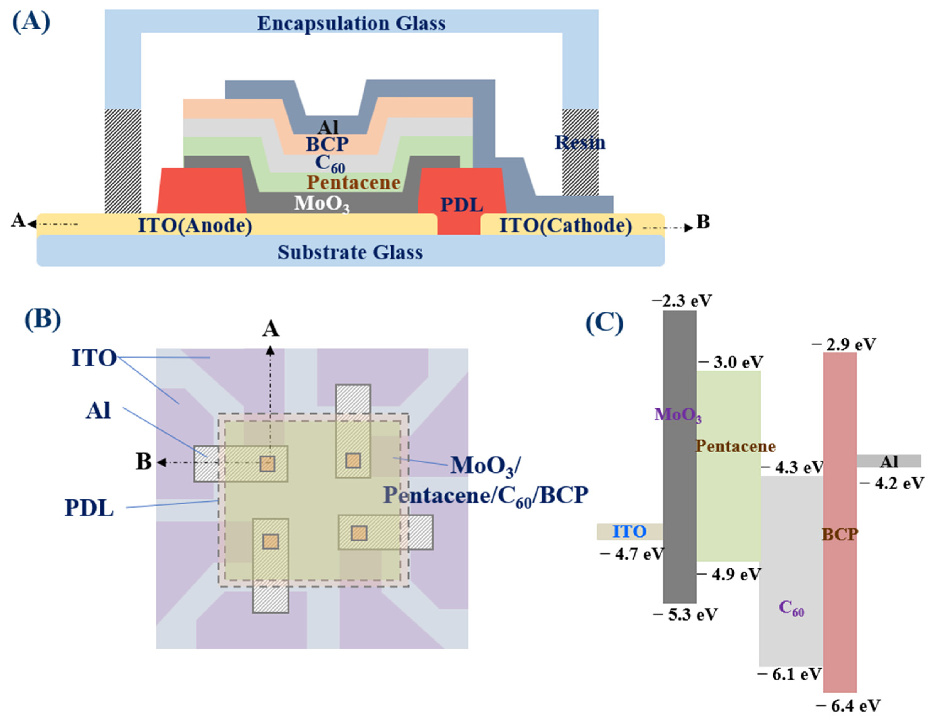
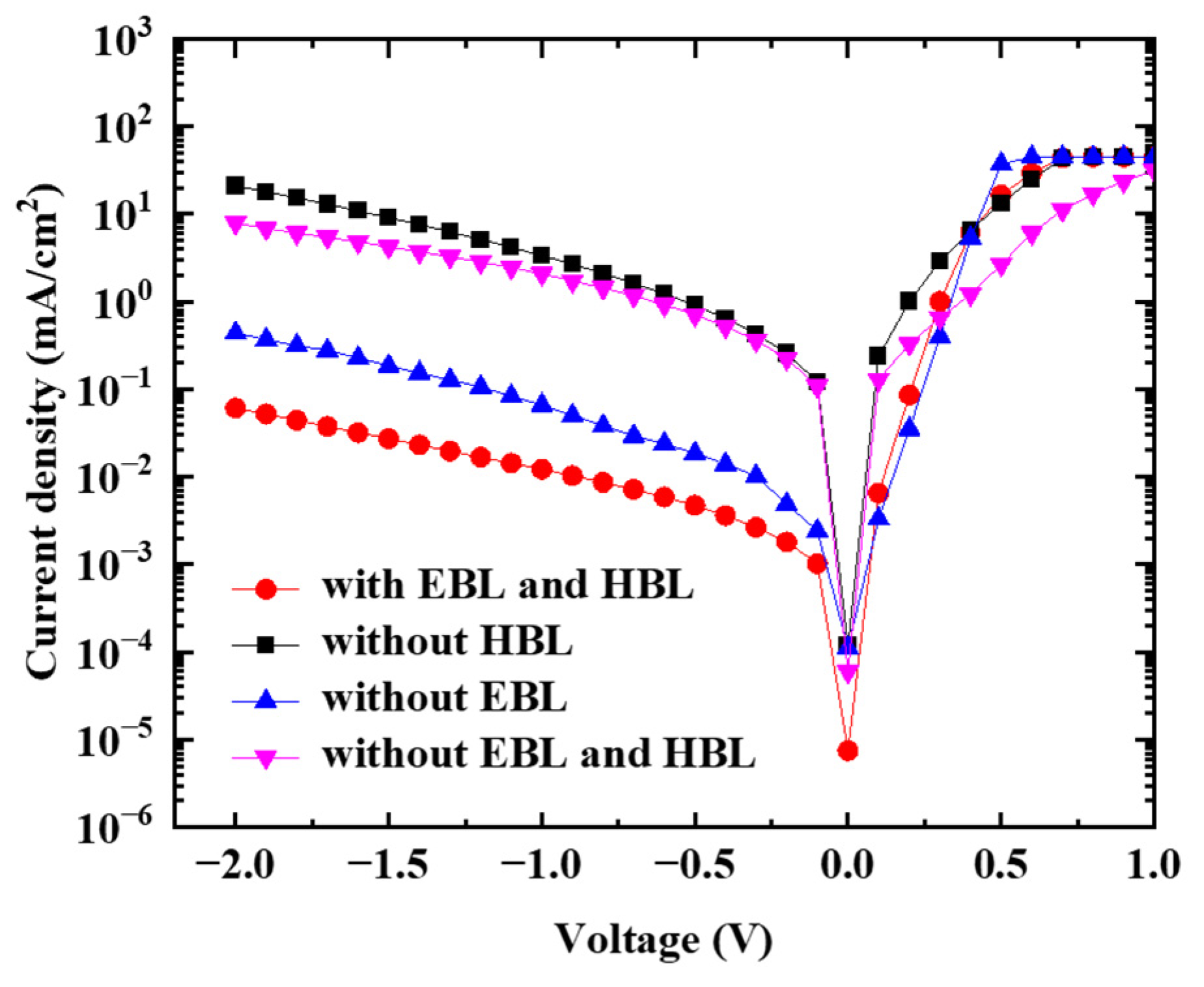
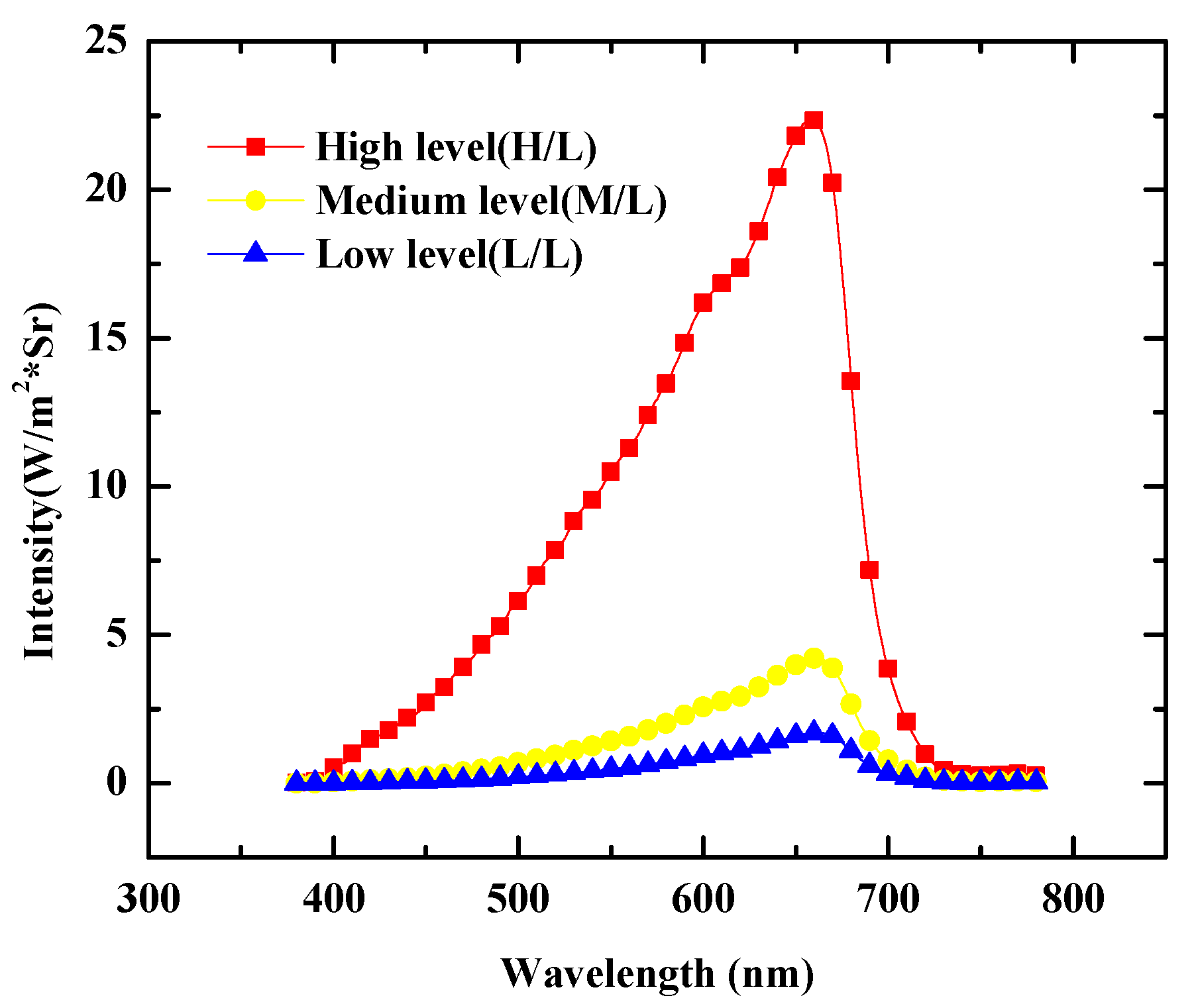
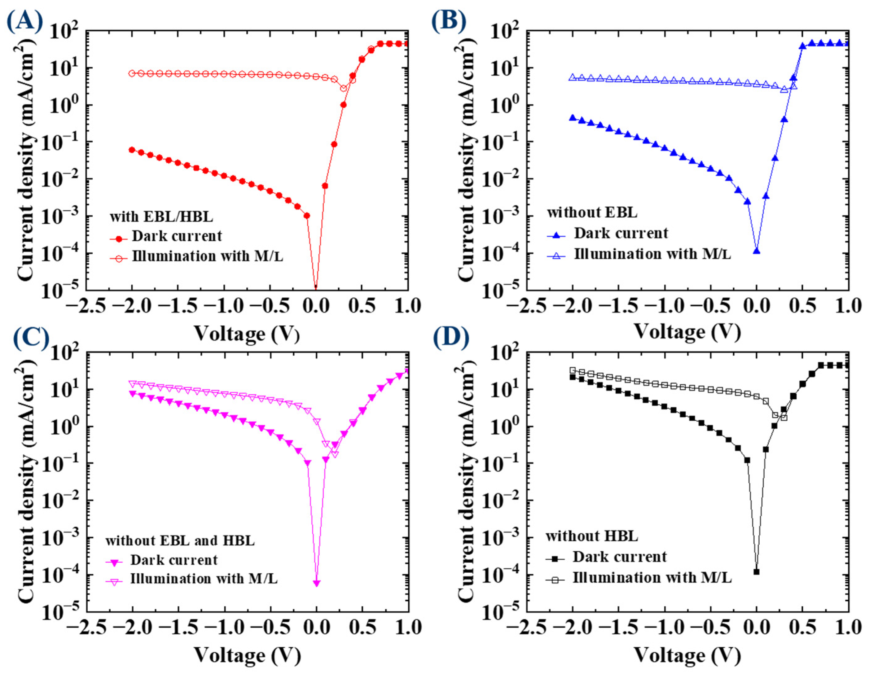
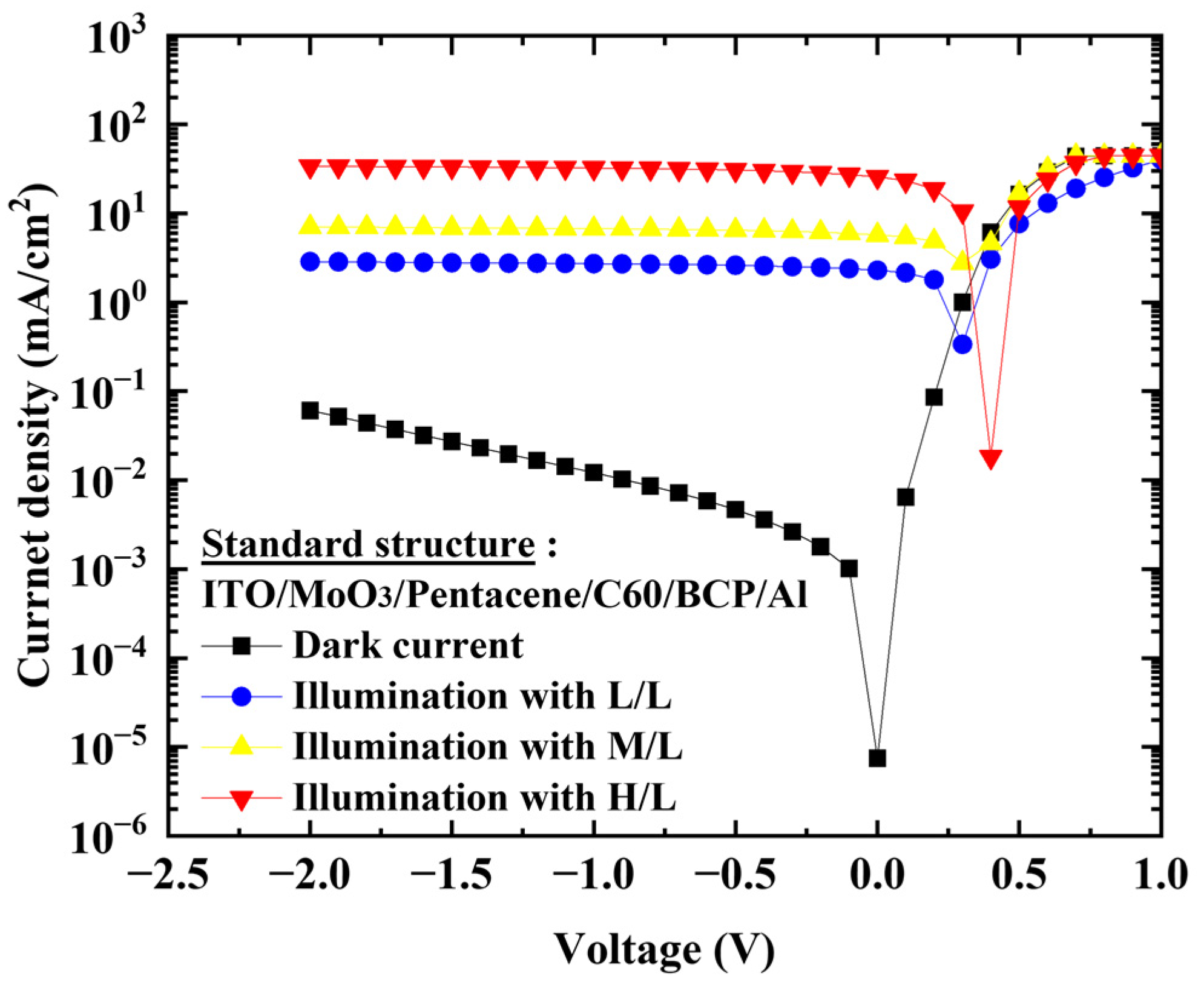
3.1. J–V Characteristics Depending on the Interfacial Layers

Figure 1A shows the standard device structure, Figure 1B shows the planar layout design, and Figure 1C shows a schematic of its estimated energy level. Figure 2 shows the dark current density–voltage (J–V) characteristics for the four types of devices, including the standard structure with the two interfacial layers of EBL and HBL. The influence of the blocking layers on the dark current becomes apparent in the J–V characteristics. The standard device structure exhibits a dark current density of 0.013 mA/cm2 at −1 V reverse bias. The OPDI devices without EBL, and without both EBL and HBL, show the dark current of (0.066 and 2.068) mA/cm2, respectively, at −1 V reverse bias. Meanwhile, the OPDI device without HBL shows the dark current of 3.347 mA/cm2 at −1 V reverse bias, which is a factor of 279 higher than that for the standard device. The results show that the HBL dominantly affects the dark current. Without the BCP HBL, the dark current density increases rapidly as the reverse bias increases, and the degree of the increased dark current is more severe than that of the device without both EBL and HBL. It is estimated that the holes injected into the active layer from the Al electrode without HBL can transport to the ITO/MoO3 layers and accumulate at the MoO3/Pentacene interface. The accumulated holes create a strong localized electric field at the MoO3/Pentacene interface, and result in the injection of electrons from the ITO anode, enhancing the dark current [22]. A low saturation current under reverse bias is an important requirement of the OPDI, and thus, the HBL and EBL interfacial layers in this device architecture are necessary. The thicknesses of the MoO3 and BPL block layers were fixed according to the most proper thicknesses (10 nm) with making reference to the literature because it should take too much time for optimizing each thickness. Thus, there will be room for obtaining the optimum figure of merit of the OPDI performance in terms of the dark current and the efficiency [23].
To quickly analyze the J–V characteristic under illumination, a Halogen lamp light source was used and the luminance spectrum is shown in Figure 3 with three illumination levels of low, medium, and high at (579.9, 1555.0, and 9791.6) W/m2, respectively. For the four types of structures, the J–V characteristics were measured under the illumination of the medium level (1555.0 W/m2) and compared with the dark current density, as shown in Figure 4. When both the HBL and EBL were used, the ratio of on-current (6.7 mA/cm2) to dark current (12.1 × 10⁻³ mA/cm2) under a reverse bias of −1 V was about 553:1, while when the HBL was omitted, the ratio was about 3.9:1 ((12.9 to 3.3) mA/cm2). Table 1 summarizes these results. Moreover, when both the HBL and EBL were used, the photocurrent level was saturated independently of the reverse bias. However, when the HBL was not used, the photocurrent was not saturated, and was affected by the dark current. For the standard OPDI with the HBL and EBL, the J–V characteristics were measured at the three illumination levels, and Figure 5 shows the results. The photocurrent responds well to the illumination levels and becomes saturated for all of them. The saturation of the current level under reverse bias is a very important requirement for the OPDI operation. It is notable that MoO3 and BCP play a good role in blocking layers and contribute to the saturated operation in this OPDI architecture.

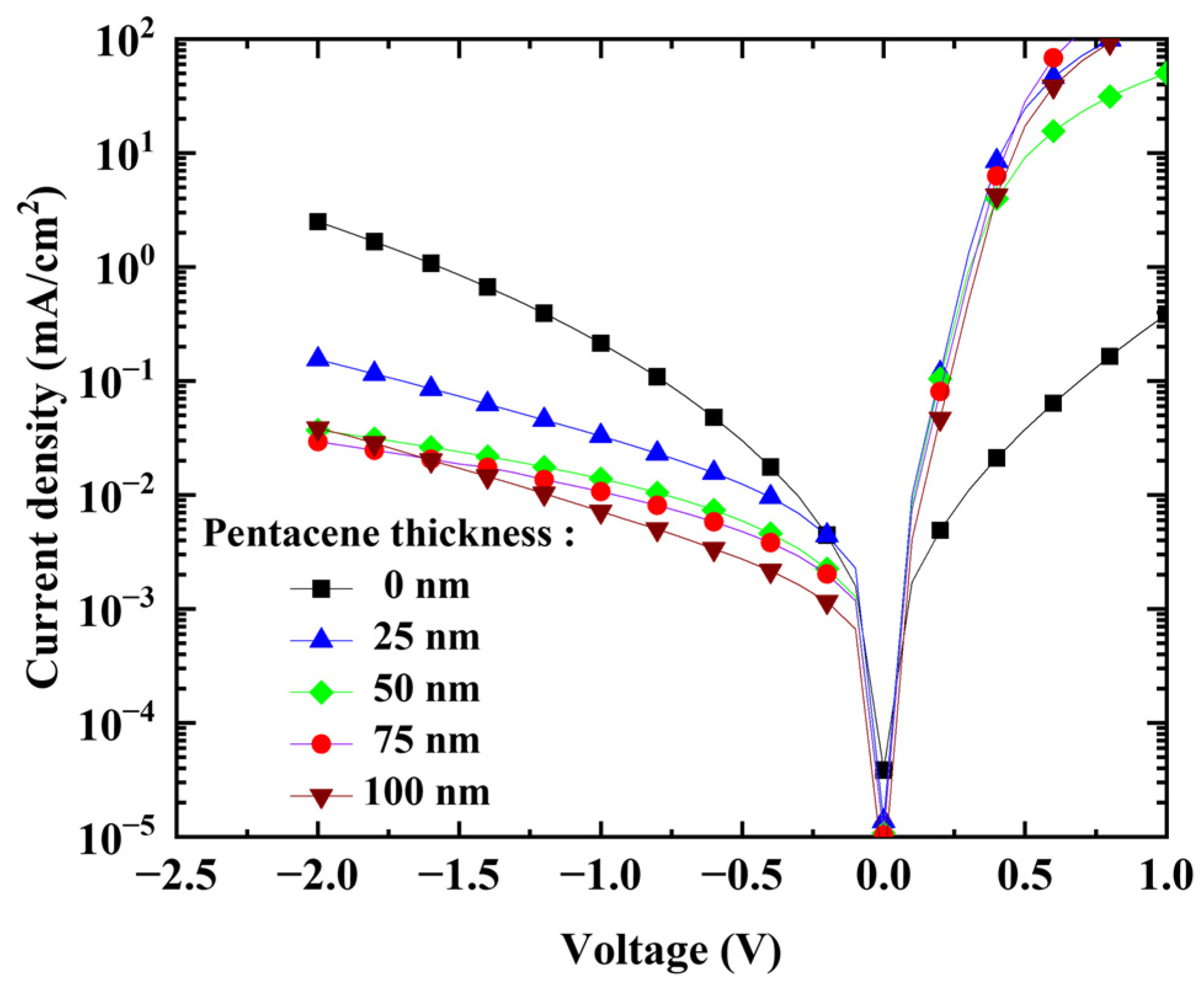
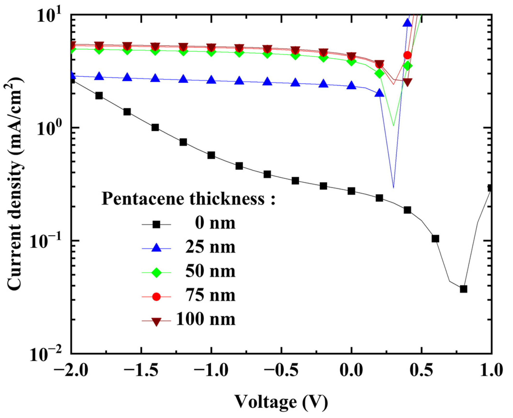
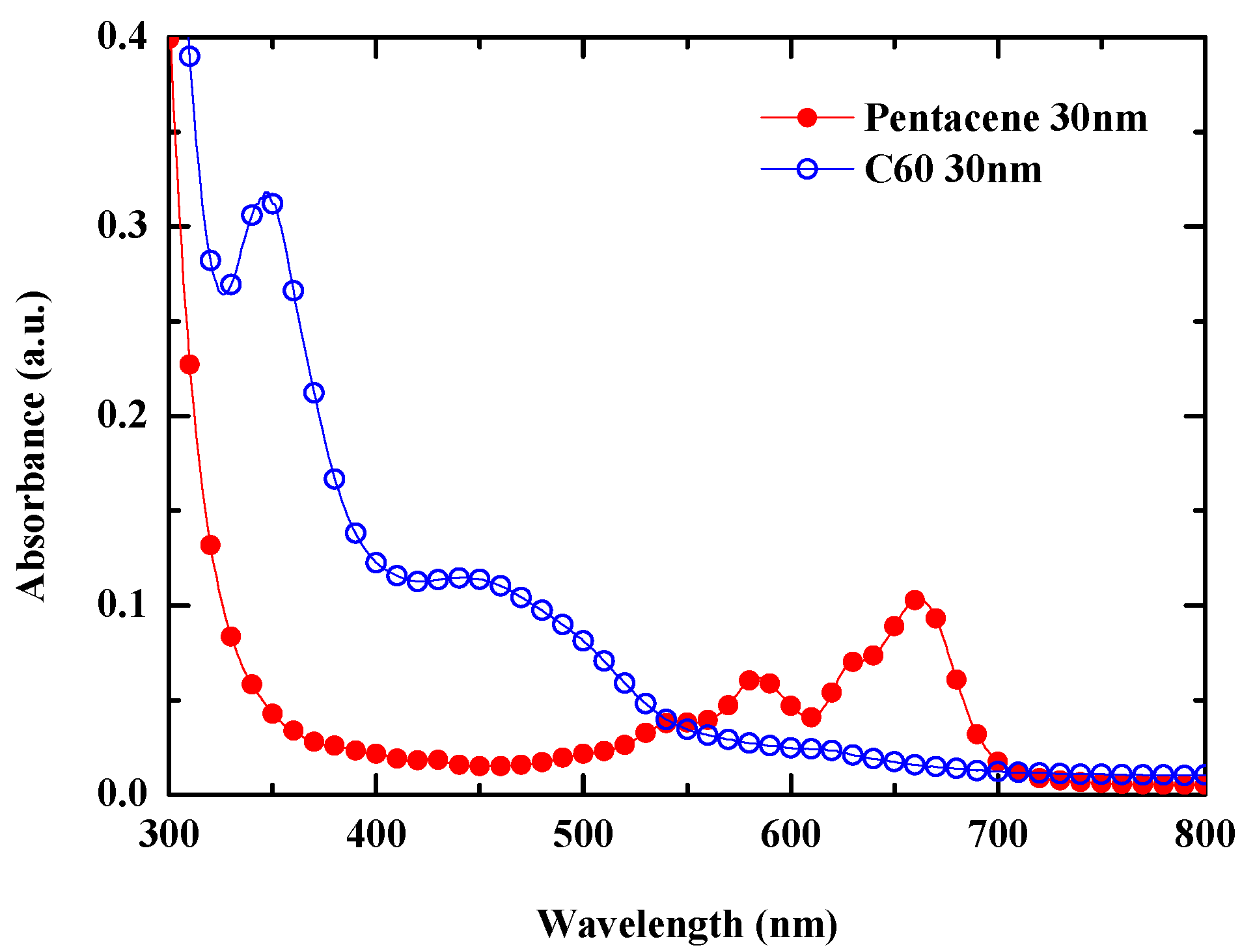
3.2. Device Performance with Variable Active Layer Thickness

In terms of the dark current and the external quantum efficiency, the thickness of the active layer plays a critical role. The dark current is a critical parameter determining the specific detectivity, which is important for the light detection function of the OPDI. Depending on the material properties and device structures, the dark current range can span several orders [24,25]. To suppress the dark current in organic diodes, several approaches have been reported in the literature [14,26,27,28]. One of the most frequently used methods is the suppression of shunt paths [29]. There are several sources of the dark current of the OPDIs, however, this remains controversial due to lack of comprehensive understanding [25,30]. The intrinsic dark current typically comprises a thermal generation of charges over the gap within the active layer, and a charge carrier injection from the metal contact into the organic semiconductor. However, in practical organic diodes, charge-transfer (CT) states are present at the donor–acceptor interface [31,32], and the effective gap for thermal generation, the characteristic charge-transfer state energy (ECT), is usually lower than the gap of the single organic semiconductor. In addition, trap states with intra-gap energies in real organic semiconductors are taken into account, usually due to the disordered nature of the organic materials, structural defects of the devices, and impurities present in the materials [33,34]. Several reports mention the influence of the trap states on the limited charge transport, increased recombination rate, and increase in the dark current [35,36,37,38].
In this study, the thickness of the p-type electron donor layer (pentacene) was varied from (25 to 100) nm. Figure 6 shows the current density–voltage characteristics under the dark condition. The dark current decreased as the thickness of the pentacene layer increased, and this may have resulted from the higher shunt resistance due to the thicker layer, and as a result, the effective suppression of electron injection by the electron-blocking layer [39,40,41].
Under the illumination condition with the medium level (Figure 3), the photocurrent of the OPDI device was dependent on the thickness of the pentacene layer, as shown in Figure 7. When the pentacene was not used, the photocurrent density was 0.57 mA/cm2 under a reverse bias of −1 V, while its dark current was 0.215 mA/cm2. Upon increasing the thickness of the pentacene layer from (50 to 75) nm, the photocurrent increased from (4.68 to 5.1) mA/cm2, while the dark current densities were (0.014 and 0.011) mA/cm2, respectively. This is attributed to the increase in the amount of absorbed light on increasing the thickness of the absorbing pentacene layer. However, for the thickness of 100 nm, the photocurrent (5.2 mA/cm2) did not increase significantly (dark current density: 0.007 mA/cm2). This may be attributed to the trade-off between two opposing effects. One is the positive effect of the increase in light absorption on the increase in thickness. The other is the negative effect of the reduction in the extraction of photo-generated charge carriers and/or the increased probability of the recombination loss of excitons due to the longer diffusion path [42]. Thus, to optimize the OPDI performance, the thickness of the pentacene layer should be finely tuned.
Figure 8A shows the external quantum efficiency (EQE) spectra with different thicknesses of the pentacene layer. The EQE is defined as the ratio between the number of incident photons and the extracted number of the photo-generated free electrons and can be expressed as:
E Q E = I p P i n h q
where Ip is the photogenerated current, Pin is the incident light intensity, h is Plank’s constant, ν is the frequency of light, and q is the electron charge.
The EQE in the wavelength range (500–700) nm increases when increasing the thickness of the pentacene layer. Exceptionally, the EQE with 25 nm pentacene exhibited a slightly higher EQE than that with 50 nm pentacene. We have conducted the experiment twice under the same condition with the pentacene thickness of 25 nm to verify the accuracy, and obtained exactly the same results, which are provided in Figure S1 of the Supporting Information (SI). According to the literature, the thickness dependence of the active layer on the photo-generated current can be attributed to a compromise between an increased absorption and a charge recombination loss due to the increase in the traveling distance of carriers with increasing the thickness of the active layer, the impact of grain size, and so on [43,44,45,46]. This paper addresses the surface morphology being affected by the grain size of the active layer, as a consequence affecting the dark current and photo-generated current. Accordingly, we have investigated the surface morphology with the thickness of the pentacene layer using secondary electron microscopy (SEM), the results of which are presented in Figure S2 of the Supporting Information (SI). To measure the surface morphology, the pentacene layer with the corresponding thickness was deposited on the glass/ITO (150 nm)/MoO3 (10 nm) layers. From the results, no grains were found on the ITO/MoO3 layers and the grain size was slightly increased in proportion to the evaporation time. Interestingly, the apparent grain boundaries appeared between grains somewhat differently depending on the thickness. All these factors will collectively influence the external quantum efficiency, depending on the thickness of the pentacene layer.
Note that the resonance wavelength is proportional to the thickness times of the effective refractive indices of the active layers between the electrodes [47,48]. Thus, by keeping the thickness of the C60 constant and increasing the thickness of the pentacene, the resonance wavelength also increases. This phenomenon can be seen clearly in Figure 9. The OPDI device without the pentacene layer shows nearly zero EQE in this range of (500–700) nm, which shows a non-resonance response. However, with the pentacene included, two EQE peaks appear in the wavelength range (350–500) nm. The first peak at (350–360) nm was almost fixed independent of the thickness of the pentacene, and the second peak, which is attributed to the resonance effect, moves to a higher wavelength upon increasing the thickness of the pentacene. When the thickness of the pentacene is 25 nm, the resonance wavelength nearly coincides with the wavelength of the maximum absorption peak without the cavity effect, resulting in absorption enhancement. That is, the EQE with the 25 nm pentacene was 56% at the wavelength of 360 nm, which was enhanced by 1.5 times compared to 39% at the wavelength of 360 nm, without the cavity effect. When the thickness of the pentacene was 75 nm, the second peak at the wavelength of 440 nm seemed to be enhanced to 40% by the second absorption peak (~21% EQE) present at the same wavelength of 440 nm without the cavity effect. The responsivity of the OPDI devices with a different thickness of the pentacene layer follows a similar trend to the EQE spectra, as shown in Figure 8B. The peak responsivity attributed to the 25 nm pentacene layer exhibited the value of 0.17 A/W at a wavelength of around 360 nm.
The responsivity is defined as the ratio of the photogenerated current to the power intensity of incident light and can be expressed as:
R = E Q E q h c
where λ is the wavelength of light in nm and c is the speed of light in vacuum.
To analyze the EQE spectra, the absorption spectra of pentacene and C60 were investigated, and Figure 9 shows the results. It is noticeable that the pentacene shows light absorption in the wavelength range (550–700) nm with a maximum peak around 660 nm, which coincides with the EQE peak around that wavelength shown in Figure 8A. The absorption spectrum of C60 shows a strong absorption in the wavelength range (300–400) nm with a maximum peak around 350 nm, which coincides with the EQE peak at this position of Figure 8A. According to the literature [49], the HOMO–LUMO transition in C60 is forbidden; instead, the vibronic transitions are allowed via anharmonic vibrations, which results in the above gap transition in the range (200–540) nm. The absorption peak at a wavelength of around 350 nm in Figure 9 coincides with that reported in this paper. Thus, we can see that the EQE peak around 350 nm in Figure 8A is attributed to C60, while the EQE peak around 660 nm comes from the pentacene. Conclusively, the movement of the second peak from (400 to 450) nm with increasing the thickness of the pentacene layer is attributed to the optical cavity effect. That is, the resonant wavelength owing to the cavity effect increases as the cumulative optical path length increases with increasing the thickness of the pentacene layer. When the pentacene was not used, the EQE spectra resembled the absorption spectrum of the C60 of Figure 9.
To further evaluate the OPDI performance, we performed more characterizations. Essentially, the fast response is important for various sensing applications of the OPDI. The rise and fall time is defined as the time interval for the photocurrent reaching from 10% up to 90% and 90% down to 10% of its maximum value. The OPDI with a pentacene layer thickness of 50 nm shows the shortest rise time of 34.1 ms and fall time of 34.25 ms under a blue (455 nm) light source at 0.71 mW/cm2, the results of which are shown in Figure 10, including the rise/fall times of 41.4/36.5 ms under red light (660 nm). This might be related to the diffusion time and the trap states depending on the active layer thickness and the morphology.
Detectivity is another important parameter for the OPDIs’ applications, which can be evaluated using the calculation as D* = R/(2qJdark)1/2 considering the shot noise from the dark current as the major contribution of total noise, where R is the responsivity, Jdark is the dark current, and q is the elementary charge. Thus, D* is the figure of merit to characterize the capability of weak light detection for the OPDI, considering both photoelectric conversion efficiency and noise current. The calculated detectivity is presented in Figure S3. It is seen that the detectivity increases from approximately 5 × 10⁸ to 1.5 × 10⁹ Jones, and the pentacene thickness increases from 25 nm to 75 nm. It decreases again at the higher thickness of 100 nm compared to that of 75 nm. The maximum detectivity was shown to be 1.45 × 10⁹ Jones at a 440 nm wavelength for the pentacene thickness of 75 nm.
In summary, we have presented work on the fabrication and characterizations of the fully small molecule-based organic photodiodes using the in-line vacuum evaporation method. With the conventional materials of pentacene as the donor and C60 as the acceptor, the EQE at a wavelength of 370 nm increased by 1.5 times via the resonance absorption enhancement, compared to the non-cavity device without the pentacene layer. The MoO3 and BCP played roles as an electron-blocking layer and hole-blocking layer, respectively, resulting in the effective suppression of the dark current. We expect further studies to focus on the performance improvements using the bulk heterojunction structure, and to extend the absorption wavelength to near-infrared (NIR) using other small molecules.

4. Conclusions

In summary, we present all small molecule-based organic photodiodes fabricated using the vacuum evaporation method, a process which can provide promising features such as a well-defined molecular structure, high purity, large scalability, and good process repeatability. As the donor and acceptor materials, the conventional pentacene and C60 were used. MoO3 and BCP played a good role as an electron-blocking layer and hole-blocking layer, respectively. In particular, the BCP layer worked as the HBL played a main role to suppress the dark current, of which the current density was reduced by two orders higher than that without the HBL.
By varying the thickness of the pentacene layer, the resonance wavelength was tuned via a cavity effect. By virtue of this effect, the light absorption at 360 nm, of which the wavelength corresponds to the maximum absorption of C60, was enhanced by 1.5 times, compared to that without the non-cavity device. To reduce the dark current and increase the responsivity, further study, such as the bulk heterojunction and the use of other small molecules, is needed, specifically to extend the absorption wavelength up to the near-infrared.

Supplementary Materials

The following supporting information can be downloaded at: https://www.mdpi.com/article/10.3390/nano13212820/s1, Figure S1: EQEs for the OPDIs experimented twice with the pentacene 25 nm; Figure S2: the surface morphology measured by SEM with the thickness of pentacene layer on ITO/MoO3. Figure S3: The detectivity with Pentacene thickness measured under −2 V reverse bias.

Author Contributions

Y.W.K. and D.L.: fabrication and investigation. Y.J. and H.Y.: conceptualization. E.-S.C.: investigation and validation. E.D.: EQE measurement and investigation. Y.-J.P. and K.-I.S.: discussion and validation. S.-J.K.: conceptualization, writing—original draft preparation, project administration, resources, and supervision. All authors have read and agreed to the published version of the manuscript.

Funding

This work was supported by a National Research Foundation of Korea (NRF) grant, funded by the Korean government (MSIT) (No. NRF-2022R1A2C1003076), and partly supported by a Korea Institute for Advancement of Technology (KIAT) grant, funded by the Korean Government (MOTIE) (No. P0012453, The Competency Development Program for Industry Specialist).

Data Availability Statement

The data that support the findings of this study are available from the corresponding author upon reasonable request.

Conflicts of Interest

The authors declare no conflict of interest.

References

  1. Ng, T.N.; Wong, W.S.; Chabinyc, M.L.; Sambandan, S.; Street, R.A. Flexible image sensor array with bulk heterojunction organic photodiode. Appl. Phys. Lett. 2008, 92, 213303. [Google Scholar] [CrossRef]
  2. Jansen-van Vuuren, R.D.; Armin, A.; Pandey, A.K.; Burn, P.L.; Meredith, P. Organic Photodiodes: The Future of Full Color Detection and Image Sensing. Adv. Mater. 2016, 28, 4766–4802. [Google Scholar] [CrossRef] [PubMed]
  3. Kamada, T.; Hatsumi, R.; Watanabe, K.; Kawashima, S.; Katayama, M.; Adachi, H.; Ishitani, T.; Kusunoki, K.; Kubota, D.; Yamazaki, S. OLED display incorporating organic photodiodes for fingerprint imaging. J. Soc. Inf. Display 2019, 27, 361–371. [Google Scholar] [CrossRef]
  4. Guo, H.T.; Saifi, S.; Fukuda, K.; Cheng, H.M.; Lou, Z.R.; Xu, X.M. Flexible organic photodetectors and their use in wearable systems. Digit. Signal Process 2022, 125, 103145. [Google Scholar] [CrossRef]
  5. Xu, H.H.; Yin, L.; Liu, C.; Sheng, X.; Zhao, N. Recent Advances in Biointegrated Optoelectronic Devices. Adv. Mater. 2018, 30, 1800156. [Google Scholar] [CrossRef]
  6. Li, N.; Eedugurala, N.; Leem, D.S.; Azoulay, J.D.; Ng, T.N. Organic Upconversion Imager with Dual Electronic and Optical Readouts for Shortwave Infrared Light Detection. Adv. Funct. Mater. 2021, 31, 2100565. [Google Scholar] [CrossRef]
  7. Shan, T.; Hou, X.; Yin, X.K.; Guo, X.J. Organic photodiodes: Device engineering and applications. Front. Optoelectron. 2022, 15, 49. [Google Scholar] [CrossRef]
  8. Shekhar, H.; Solomeshch, O.; Liraz, D.; Tessler, N. Low dark leakage current in organic planar heterojunction photodiodes. Appl. Phys. Lett. 2017, 111, 223301. [Google Scholar] [CrossRef]
  9. Fallahpour, A.H.; Kienitz, S.; Lugli, P. Origin of Dark Current and Detailed Description of Organic Photodiode Operation under Different Illumination Intensities. IEEE Tran. Electron. Dev. 2017, 64, 2649–2654. [Google Scholar] [CrossRef]
  10. Lv, L.; Yu, J.D.; Sui, X.Y.; Wu, J.F.; Dong, X.H.; Lu, G.H.; Liu, X.F.; Peng, A.D.; Huang, H. Significant enhancement of responsivity of organic photodetectors upon molecular engineering. J. Mater. Chem. C 2019, 7, 5739–5747. [Google Scholar] [CrossRef]
  11. Nath, D.; Dey, P.; Joseph, A.M.; Rakshit, J.K.; Roy, J.N. CuPc/C-60 heterojunction for high responsivity zero bias organic red light photodetector. Appl. Phys. A-Mater. 2020, 126, 627. [Google Scholar] [CrossRef]
  12. Huang, Y.C.; Huang, Z.H.; Wang, T.Y.; Chaudhary, P.; Hsu, J.F.; Lee, K.M. A promising non-fullerene acceptor for near-infrared organic photodetectors operating with low dark current and high response speed. Chem. Eng. J. 2023, 464, 142633. [Google Scholar] [CrossRef]
  13. Keivanidis, P.E.; Ho, P.K.H.; Friend, R.H.; Greenham, N.C. The Dependence of Device Dark Current on the Active-Layer Morphology of Solution-Processed Organic Photodetectors. Adv. Funct. Mater. 2010, 20, 3895–3903. [Google Scholar] [CrossRef]
  14. Valouch, S.; Hones, C.; Kettlitz, S.W.; Christ, N.; Do, H.; Klein, M.F.G.; Kalt, H.; Colsmann, A.; Lemmer, U. Solution processed small molecule organic interfacial layers for low dark current polymer photodiodes. Org. Electron. 2012, 13, 2727–2732. [Google Scholar] [CrossRef]
  15. Huang, X.D.; Zhao, Z.M.; Chung, S.; Cho, K.L.; Lv, J.; Lu, S.R.; Kan, Z.P. Balancing the performance and stability of organic photodiodes with all-polymer active layers. J. Mater. Chem. C 2022, 10, 17502–17511. [Google Scholar] [CrossRef]
  16. Park, J.B.; Ha, J.W.; Yoon, S.C.; Lee, C.; Jung, I.H.; Hwang, D.H. Visible-Light-Responsive High-Detectivity Organic Photodetectors with a 1 mu m Thick Active Layer. ACS Appl. Mater. Int. 2018, 10, 38294–38301. [Google Scholar] [CrossRef]
  17. Zhang, Z.Z.; Lin, Y.Z. Organic Semiconductors for Vacuum-Deposited Planar Heterojunction Solar Cells. ACS Omega 2020, 5, 24994–24999. [Google Scholar] [CrossRef] [PubMed]
  18. Yang, D.Z.; Zhou, X.K.; Ma, D.G. Fast response organic photodetectors with high detectivity based on rubrene and C60. Org. Electron. 2013, 14, 3019–3023. [Google Scholar] [CrossRef]
  19. Ren, H.; Chen, J.D.; Li, Y.Q.; Tang, J.X. Recent Progress in Organic Photodetectors and their Applications. Adv. Sci. 2021, 8, 2002418. [Google Scholar] [CrossRef]
  20. Bonifacio, V.D.B.; Pires, R.F. Photodiodes: Principles and recent advances. J. Mater. NanoScience 2019, 6, 38–46. [Google Scholar]
  21. Xie, B.M.; Chen, Z.X.; Ying, L.; Huang, F.; Cao, Y. Near-infrared organic photoelectric materials for light-harvesting systems: Organic photovoltaics and organic photodiodes. Infomat 2020, 2, 57–91. [Google Scholar] [CrossRef]
  22. Guo, D.C.; Yang, D.Z.; Zhao, J.C.; Vadim, A.; Ma, D.G. Role of interfaces in controlling charge accumulation and injection in the photodetection performance of photomultiplication-type organic photodetectors. J. Mater. Chem. C 2020, 8, 9024–9031. [Google Scholar] [CrossRef]
  23. Yoo, S.; Potscavage, W.J.; Domercq, B.; Han, S.H.; Li, T.D.; Jones, S.C.; Szoszkiewicz, R.; Levi, D.; Riedo, E.; Marder, S.R.; et al. Analysis of improved photovoltaic properties of pentacene/C60 organic solar cells:: Effects of exciton blocking layer thickness and thermal annealing. Solid State Electron. 2007, 51, 1367–1375. [Google Scholar] [CrossRef]
  24. Kielar, M.; Dhez, O.; Pecastaings, G.; Curutchet, A.; Hirsch, L. Long-Term Stable Organic Photodetectors with Ultra Low Dark Currents for High Detectivity Applications. Sci. Rep. 2016, 6, 39201. [Google Scholar] [CrossRef] [PubMed]
  25. Simone, G.; Dyson, M.J.; Weijtens, C.H.L.; Meskers, S.C.J.; Coehoorn, R.; Janssen, R.A.J.; Gelinck, G.H. On the Origin of Dark Current in Organic Photodiodes. Adv. Opt. Mater. 2020, 8, 1901568. [Google Scholar] [CrossRef]
  26. Gong, X.O.; Tong, M.H.; Park, S.H.; Liu, M.; Jen, A.; Heeger, A.J. Semiconducting Polymer Photodetectors with Electron and Hole-blocking Layers: High Detectivity in the Near-Infrared. Sensors 2010, 10, 6488–6496. [Google Scholar] [CrossRef]
  27. Friedel, B.; Keivanidis, P.E.; Brenner, T.J.K.; Abrusci, A.; McNeill, C.R.; Friend, R.H.; Greenham, N.C. Effects of Layer Thickness and Annealing of PEDOT:PSS Layers in Organic Photodetectors. Macromolecules 2009, 42, 6741–6747. [Google Scholar] [CrossRef]
  28. Zheng, Y.C.; Fischer, A.; Sergeeva, N.; Reineke, S.; Mannsfeld, S.C.B. Exploiting lateral current flow due to doped layers in semiconductor devices having crossbar electrodes. Org. Electron. 2019, 65, 82–90. [Google Scholar] [CrossRef]
  29. Tang, Z.; Ma, Z.F.; Sanchez-Diaz, A.; Ullbrich, S.; Liu, Y.; Siegmund, B.; Mischok, A.; Leo, K.; Campoy-Quiles, M.; Li, W.W.; et al. Polymer: Fullerene Bimolecular Crystals for Near-Infrared Spectroscopic Photodetectors. Adv. Mater. 2017, 29, 1702184. [Google Scholar] [CrossRef]
  30. Kublitski, J.; Hofacker, A.; Boroujeni, B.K.; Benduhn, J.; Nikolis, V.C.; Kaiser, C.; Spoltore, D.; Kleemann, H.; Fischer, A.; Ellinger, F.; et al. Reverse dark current in organic photodetectors and the major role of traps as source of noise. Nat. Commun. 2021, 12, 551. [Google Scholar] [CrossRef]
  31. Kaiser, C.; Schellhammer, K.S.; Benduhn, J.; Siegmund, B.; Tropiano, M.; Kublitski, J.; Spoltore, D.; Panhans, M.; Zeika, O.; Ortmann, F.; et al. Manipulating the Charge Transfer Absorption for Narrowband Light Detection in the Near-Infrared. Chem. Mater. 2019, 31, 9325–9330. [Google Scholar] [CrossRef]
  32. Kyndiah, A.; Cramer, T.; Albonetti, C.; Liscio, F.; Chiodini, S.; Murgia, M.; Biscarini, F. Charge Transfer and Percolation in C60/Pentacene Field-Effect Transistors. Adv. Electron. Mater. 2015, 1, 1400036. [Google Scholar] [CrossRef]
  33. Kang, J.H.; da Silva, D.; Bredas, J.L.; Zhu, X.Y. Shallow trap states in pentacene thin films from molecular sliding. Appl. Phys. Lett. 2005, 86, 152115. [Google Scholar] [CrossRef]
  34. Nicolai, H.T.; Kuik, M.; Wetzelaer, G.A.H.; de Boer, B.; Campbell, C.; Risko, C.; Bredas, J.L.; Blom, P.W.M. Unification of trap-limited electron transport in semiconducting polymers. Nat. Mater. 2012, 11, 882–887. [Google Scholar] [CrossRef] [PubMed]
  35. Sergeeva, N.; Ullbrich, S.; Hofacker, A.; Koerner, C.; Leo, K. Structural Defects in Donor-Acceptor Blends: Influence on the Performance of Organic Solar Cells. Phys. Rev. Appl. 2018, 9, 024039. [Google Scholar] [CrossRef]
  36. Cowan, S.R.; Leong, W.L.; Banerji, N.; Dennler, G.; Heeger, A.J. Identifying a Threshold Impurity Level for Organic Solar Cells: Enhanced First-Order Recombination via Well-Defined PC84BM Traps in Organic Bulk Heterojunction Solar Cells. Adv. Funct. Mater. 2011, 21, 3083–3092. [Google Scholar] [CrossRef]
  37. Hofacker, A.; Neher, D. Dispersive and steady-state recombination in organic disordered semiconductors. Phys. Rev. B 2017, 96. [Google Scholar] [CrossRef]
  38. Wu, Z.H.; Li, N.; Eedugurala, N.; Azoulay, J.D.; Leem, D.S.; Ng, T.N. Noise and detectivity limits in organic shortwave infrared photodiodes with low disorder. NPJ Flex. Electron. 2020, 4, 6. [Google Scholar] [CrossRef]
  39. Yoon, S.; Ha, J.; Sim, K.M.; Cho, W.; Chung, D.S. Systematic optimization of low bandgap polymer/[6,6]-phenyl C-70 butyric acid methyl ester blend photodiode via structural engineering. Org. Electron. 2016, 35, 17–23. [Google Scholar] [CrossRef]
  40. Lee, C.C.; Estrada, R.; Li, Y.Z.; Biring, S.; Al Amin, N.R.A.; Li, M.Z.; Liu, S.W.; Wong, K.T. Vacuum-Processed Small Molecule Organic Photodetectors with Low Dark Current Density and Strong Response to Near-Infrared Wavelength. Adv. Opt. Mater. 2020, 8, 2000519. [Google Scholar] [CrossRef]
  41. Simone, G.; Dyson, M.J.; Meskers, S.C.J.; Janssen, R.A.J.; Gelinck, G.H. Organic Photodetectors and their Application in Large Area and Flexible Image Sensors: The Role of Dark Current. Adv. Funct. Mater. 2020, 30, 1904205. [Google Scholar] [CrossRef]
  42. Credgington, D.; Kim, Y.; Labram, J.; Anthopoulos, T.D.; Durrant, J.R. Analysis of Recombination Losses in a Pentacene/C-60 Organic Bilayer Solar Cell. J. Phys. Chem. Lett. 2011, 2, 2759–2763. [Google Scholar] [CrossRef]
  43. Lenes, M.; Koster, L.J.A.; Mihailetchi, V.D.; Blom, P.W.M. Thickness dependence of the efficiency of polymer: Fullerene bulk heterojunction solar cells. Appl. Phys. Lett. 2006, 88, 243502. [Google Scholar] [CrossRef]
  44. Nam, Y.M.; Huh, J.; Jo, W.H. Optimization of thickness and morphology of active layer for high performance of bulk-heterojunction organic solar cells. Sol. Energ. Mat. Sol. Cells 2010, 94, 1118–1124. [Google Scholar] [CrossRef]
  45. Chaudhary, S.; Yadav, V.; Singh Negi, C.M.; Gupta, S.K. Active layer thickness dependence of optoelectronic performance in CH3NH3PbI3 perovskite-based planar heterojunction photodiodes. Opt. Mater. 2020, 106, 109960. [Google Scholar] [CrossRef]
  46. Nath, D.; Dey, P.; Joseph, A.M.; Rakshit, J.K.; Roy, J.N. Zero bias high responsive visible organic photodetector based on pentacene and C-60. Opt. Laser Technol. 2020, 131, 106393. [Google Scholar] [CrossRef]
  47. Yang, J.J.; Huang, J.; Li, R.M.; Li, H.; Sun, B.; Lin, Q.Q.; Wang, M.; Ma, Z.F.; Vandewal, K.; Tang, Z. Cavity-Enhanced Near-Infrared Organic Photodetectors Based on a Conjugated Polymer Containing [1,2,5]Selenadiazolo[3,4-c]Pyridine. Chem. Mater. 2021, 33, 5147–5155. [Google Scholar] [CrossRef]
  48. Wang, Y.Z.; Siegmund, B.; Tang, Z.; Ma, Z.F.; Kublitski, J.; Xing, S.; Nikolis, V.C.; Ullbrich, S.; Li, Y.G.; Benduhn, J.; et al. Stacked Dual-Wavelength Near-Infrared Organic Photodetectors. Adv. Opt. Mater. 2021, 9, 2001784. [Google Scholar] [CrossRef]
  49. Skumanich, A. Optical-Absorption Spectra of Carbon 60 Thin-Films from 0.4 to 6.2 Ev. Chem. Phys. Lett. 1991, 182, 486–490. [Google Scholar] [CrossRef]
Figure 1. (A) The standard device structure, (B) layout, and (C) schematic of the estimated energy.
Nanomaterials 13 02820 g001
Figure 2. The dark current density–voltage (J–V) characteristics for the four types of devices, including the standard structure with the two interfacial layers of EBL and HBL.
Nanomaterials 13 02820 g002
Figure 3. The luminance spectrum of the Halogen lamp light source used with three illumination levels of low, medium, and high at (579.9, 1555.0, and 9791.6) W/m2, respectively.
Nanomaterials 13 02820 g003
Figure 4. J–V characteristics under the illumination of the medium level compared with the dark current for the device (A) with EBL and HBL, (B) without EBL, (C) without EBL and HBL, and (D) without HBL.
Nanomaterials 13 02820 g004
Figure 5. J–V characteristics measured at the three illumination levels for the standard OPDI with HBL and EBL.
Nanomaterials 13 02820 g005
Figure 6. J–V characteristics with pentacene thickness measured under dark condition.
Nanomaterials 13 02820 g006
Figure 7. J–V characteristics with pentacene thickness measured under medium illumination level.
Nanomaterials 13 02820 g007
Figure 8. (A) External quantum efficiency and (B) responsivity with pentacene thickness measured under −2 V reverse bias.
Nanomaterials 13 02820 g008
Figure 9. The measured absorption spectra of the pentacene and C60.
Nanomaterials 13 02820 g009
Figure 10. Normalized transient photocurrent measured under (A) 455 nm blue light and (B) 660 nm red light at 0.71 mW/cm2 and V = 0 V.
Nanomaterials 13 02820 g010
Table 1. Comparisons of the dark current, on-current, and On/Off ratio, depending on the device type.
Device TypeWith Block Layersw/o HBLw/o EBLw/o HBL and EBL
Current
Dark current
(−1 V reversed)
−0.01217 mA/cm2−3.34673 mA/cm2−0.06581 mA/cm2−2.0675 mA/cm2
Medium illumination
(−1 V reversed)
−6.73462 mA/cm2−12.9272 mA/cm2−4.42037 mA/cm2−7.64342 mA/cm2
On/Off Ratio×553.38×3.86×67.17×3.70
Disclaimer/Publisher’s Note: The statements, opinions and data contained in all publications are solely those of the individual author(s) and contributor(s) and not of MDPI and/or the editor(s). MDPI and/or the editor(s) disclaim responsibility for any injury to people or property resulting from any ideas, methods, instructions or products referred to in the content.

