Article

The Impact of Ambient Temperature on Electrothermal Characteristics in Stacked Nanosheet Transistors with Multiple Lateral Stacks

1
Integrated Circuit Advanced Process R&D Center, Institute of Microelectronics of the Chinese Academy of Sciences, Beijing 100029, China
2
State Key Lab of Fabrication Technologies for Integrated Circuits, Institute of Microelectronics of the Chinese Academy of Sciences, Beijing 100029, China
3
School of Integrated Circuits, University of Chinese Academy of Sciences, Beijing 100049, China
4
Process Integration, Beijing Superstring Academy of Memory Technology, Beijing 100176, China
*
Author to whom correspondence should be addressed.
Nanomaterials 2023, 13(22), 2971; https://doi.org/10.3390/nano13222971
Submission received: 22 October 2023 / Revised: 4 November 2023 / Accepted: 13 November 2023 / Published: 18 November 2023
(This article belongs to the Section Nanoelectronics, Nanosensors and Devices)

Abstract

:
With characteristic size scaling down to the nanoscale range, the confined geometry exacerbates the self-heating effect (SHE) in nanoscale devices. In this paper, the impact of ambient temperature (Tamb) on the SHE in stacked nanosheet transistors is investigated. As the number of lateral stacks (Nstack) increases, the nanoscale devices show more severe thermal crosstalk issues, and the current performance between n- and p-type nanoscale transistors exhibits different degradation trends. To compare the effect of different Tamb ranges, the temperature coefficients of current per stack and threshold voltage are analyzed. As the Nstack increases from 4 to 32, it is verified that the zero-temperature coefficient bias point (VZTC) decreases significantly in p-type nanoscale devices when Tamb is above room temperature. This can be explained by the enhanced thermal crosstalk. Then, the gate length-dependent electrothermal characteristics with different Nstacks are investigated at various Tambs. To explore the origin of drain current variation, the temperature-dependent backscattering model is utilized to explain the variation. At last, the simulation results verify the impact of Tamb on the SHE. The study provides an effective design guide for stacked nanosheet transistors when considering multiple stacks in circuit applications.

1. Introduction

With the characteristic size of integrated circuits (ICs) scaling down to the nanoscale range, the core transistor structures have gradually evolved into gate-all-around nanosheet FET (GAA NSFET) [1]. The GAA structure exhibits excellent electrostatic performance compared to FinFET technology [2]. At the same time, the nanosheet channel with a vertically stacked structure shows great performance advantages [3]. However, the confined geometry and low thermal conductivity materials, such as gate oxide and HfO2, greatly hinder heat transport, leading to a severe self-heating effect (SHE) [4,5,6,7]. The thermal conductivity of Si active regions decreases significantly due to intensified phonon scattering. Then, the thermal conductivity of the source/drain (S/D) causes an additional decrease due to heavy doping and the SiGe alloy material adopted. In addition, the nanosheet channels are floated and isolated from the substrate, making it difficult to transport heat. Due to the gate stack structure, phonon-boundary scattering is intensified. These factors lead to SHE issues being prominent in NSFET. The SHE can cause degradation of electrical performance and bring about reliability issues, ultimately decreasing the device’s lifetime significantly [8,9,10,11,12]. Some researchers have conducted a series of investigations into SHE issues, including compact models, optimization technologies, and self-heating mechanisms [13,14,15,16,17,18,19]. In addition, the multiple lateral stacks are fabricated in NSFETs for high performance. The self-heating will be exacerbated due to the rising current in the lateral stack structure [7]. This is one aspect of thermal issues.
On the other hand, the core transistors work in practical application circuits. The electrical performance is inevitably affected by ambient temperature (Tamb), where the Tamb includes those from inside the chip and the surrounding environment. The high Tamb can change the temperature-sensitivity threshold voltage (Vth) and introduce variability in the on-state current. At the same time, the Tamb plays a crucial role in thermal properties, such as thermal conductivity, lattice temperature rise, and thermal resistance (Rth) [20,21,22,23,24,25]. Some researchers have analyzed the electrothermal characteristics of FinFETs with multiple fins under the impact of Tamb [20,23,26]. However, few studies focus on the research of Tamb on NSFET with different numbers of lateral stacks (Nstack). In addition, there are few works on the geometry effect in NSFETs with different Nstacks. Therefore, we performed a symmetrical investigation on the electrothermal performance of NSFETs with different Nstacks under the Tamb impact. Furthermore, the geometry effect with different Nstacks is also studied.
In this paper, the Tamb-dependent SHE in NSFETs with different Nstacks is symmetrically measured and analyzed. The rest of the article is divided into three parts. Section 2 discusses the fabrication of NMOS and PMOS in detail. In Section 3, the current variation with different Nstacks is explored. Then, the geometry effect with different gate lengths is further analyzed based on the backscattering model. In addition, the simulations are conducted for verification. Finally, the conclusion is given in Section 4.

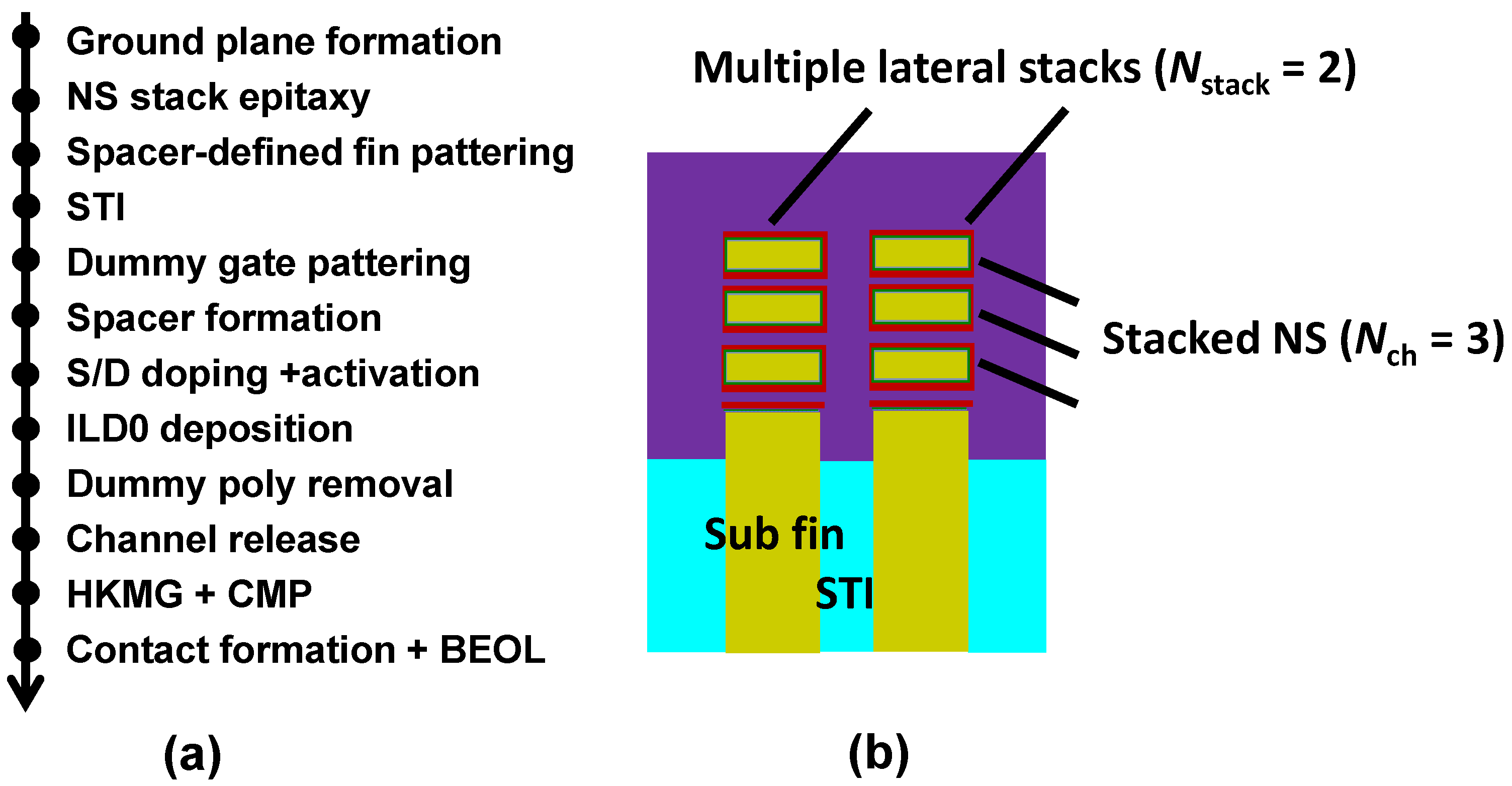
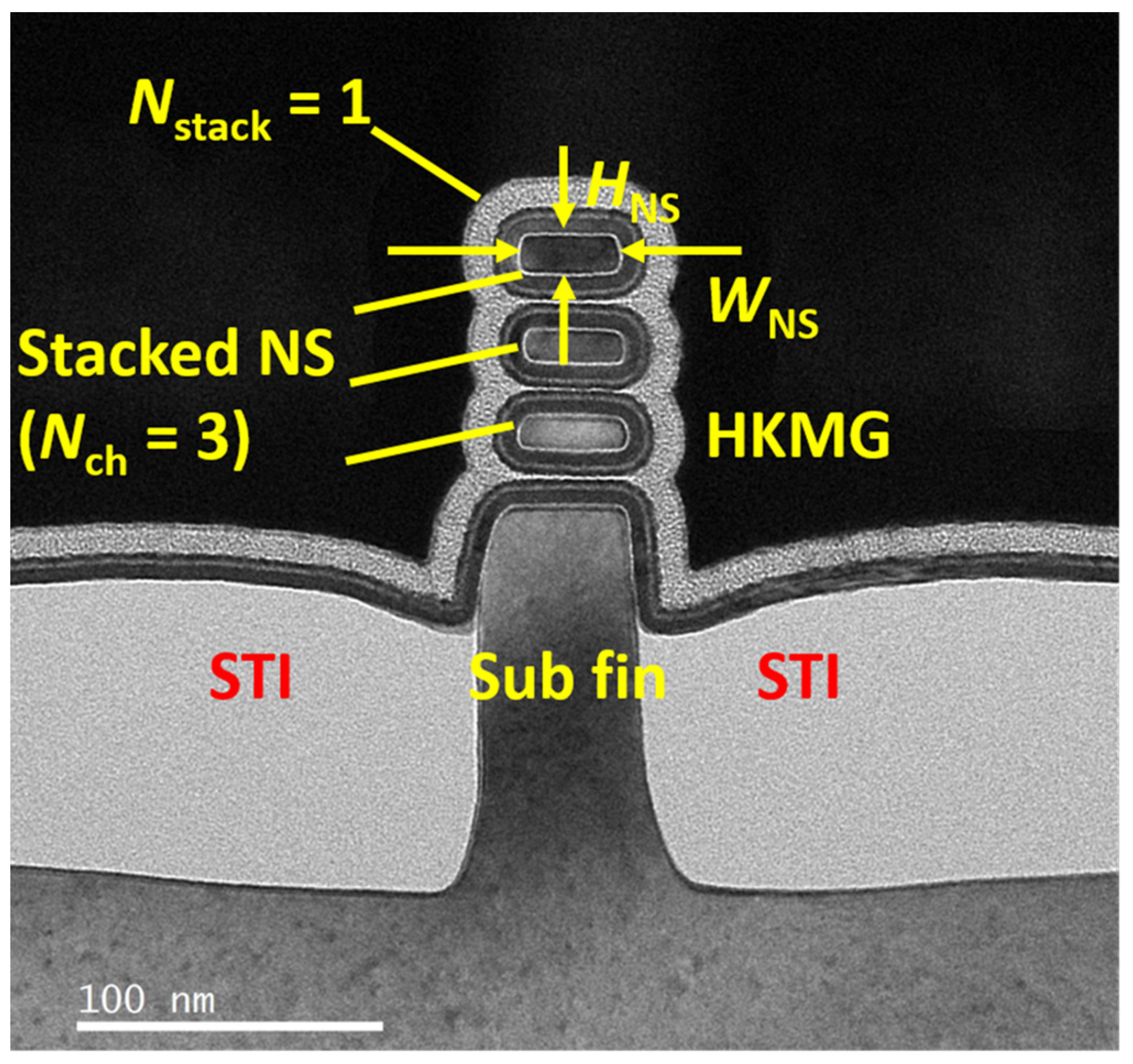
2. Device Fabrication

The integration process flow design of the NSFET is summarized in Figure 1a, where the NSFET was grown on {100} bulk Si substrates. This process flow is based on the conventional fabrication process [27]. The fabrication adopts the gate last process. Before the stacked nanosheets were formed, B and P were implanted to suppress the bottom parasitic channel in the ground plane process for NMOS and PMOS, respectively [28]. The stacked GeSi/Si layers were formed using the epitaxy process. The nanosheet channels are stacked vertically with three layers (Nch = 3). In this step, the reduced pressure chemical vapor deposition was used to grow the periodical GeSi/Si multilayer with 16 nm Ge0.3Si0.7 and 10 nm Si. Then, the fin array was carried out using spacer image transfer (SIT) technology, which was formed using a SiNx hard mask. For high-performance desire, the stacked nanosheets were fabricated with multiple lateral stacks in this step, as shown in Figure 1b. The number of parallel nanorails of lateral stacks is defined as Nstack. The Nstack is 2, 4, 8, 16, and 32. Next, the shallow trench isolation (STI) was formed to decrease the leakage current between the devices. Meanwhile, the rapid annealing process was performed to make the film compact. Then, a dummy gate was fabricated with amorphous Si to protect the nanosheets. After the deposition of amorphous Si, the chemical mechanical planarization (CMP) was used to perform the planarization process. The dummy gate image was formed using deposition and etch of Si3N4 hard mask. The inner spacer formation was a key process that was deposited using SiNx and etched using reactive ion etching (RIE). After this, the in-situ doping process with highly doped doses and the activation process were carried out to form S/D. The zero-level interlayer dielectric (ILD0) with SiNx is used to avoid the over-etch phenomenon. After the dummy gate removal, GeSi was selectively removed using the wet-etched technique. After forming the thin gate oxide layer, the HfO2 was deposited and the nanosheet was surrounded by different metal stacks. The atom-layer-deposition technology (ALD) was used to deposit the multilayer HK/MG films, and the CMP was performed to achieve gate separation. Finally, the tungsten contact and the BEOL process were fabricated to complete the NSFETs.
Through the measurement of transmission electron microscopy (TEM), Figure 2 shows the fabricated channel structure of NSFETs, which can be seen that the NSFETs are successfully fabricated according to the process flow. The nanosheets are separated using HK/MG, and the STI is formed near the sub-fin. The width of the sub-fin is similar to that of the nanosheet. The nanosheet width (WNS) is about 30 nm, and the nanosheet thickness (TNS) is about 10 nm. The gate length (LG) is 30, 40, 60, and 500 nm. Then, energy-dispersive spectroscopy (EDS) is used to exhibit the distribution of elements in NSFETs, as shown in Figure 3. It shows that Ge has been completely removed, and the nanosheets are separated from each other. Each nanosheet is surrounded by Hf and oxide elements. This indicates that the nanosheets can be well controlled using bias voltages. At the same time, it can be seen that Al, Ti, N, and Ta elements are deposited surrounding the nanosheets, and the W element has been wrapped to the Si nanosheets.

3. Results and Discussion

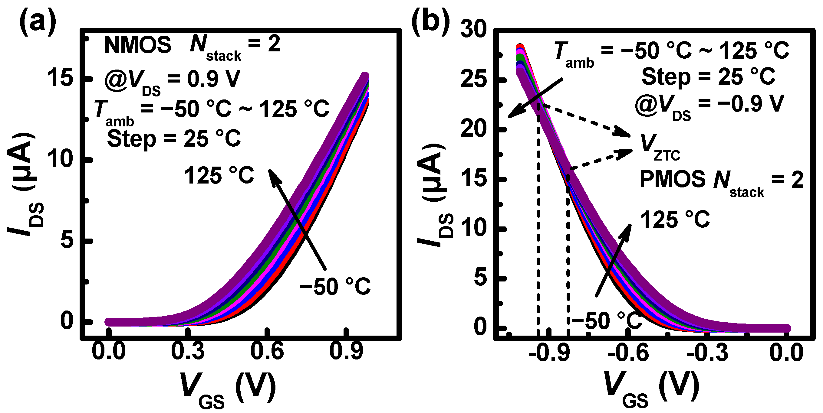
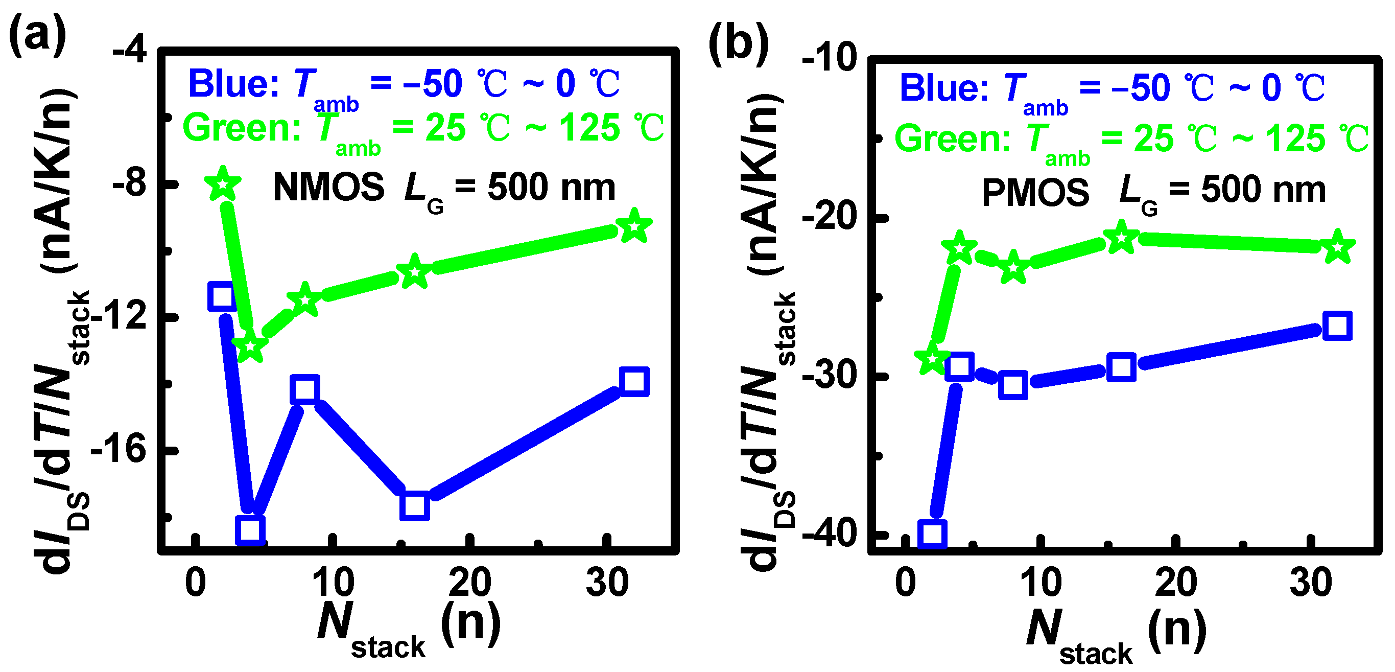
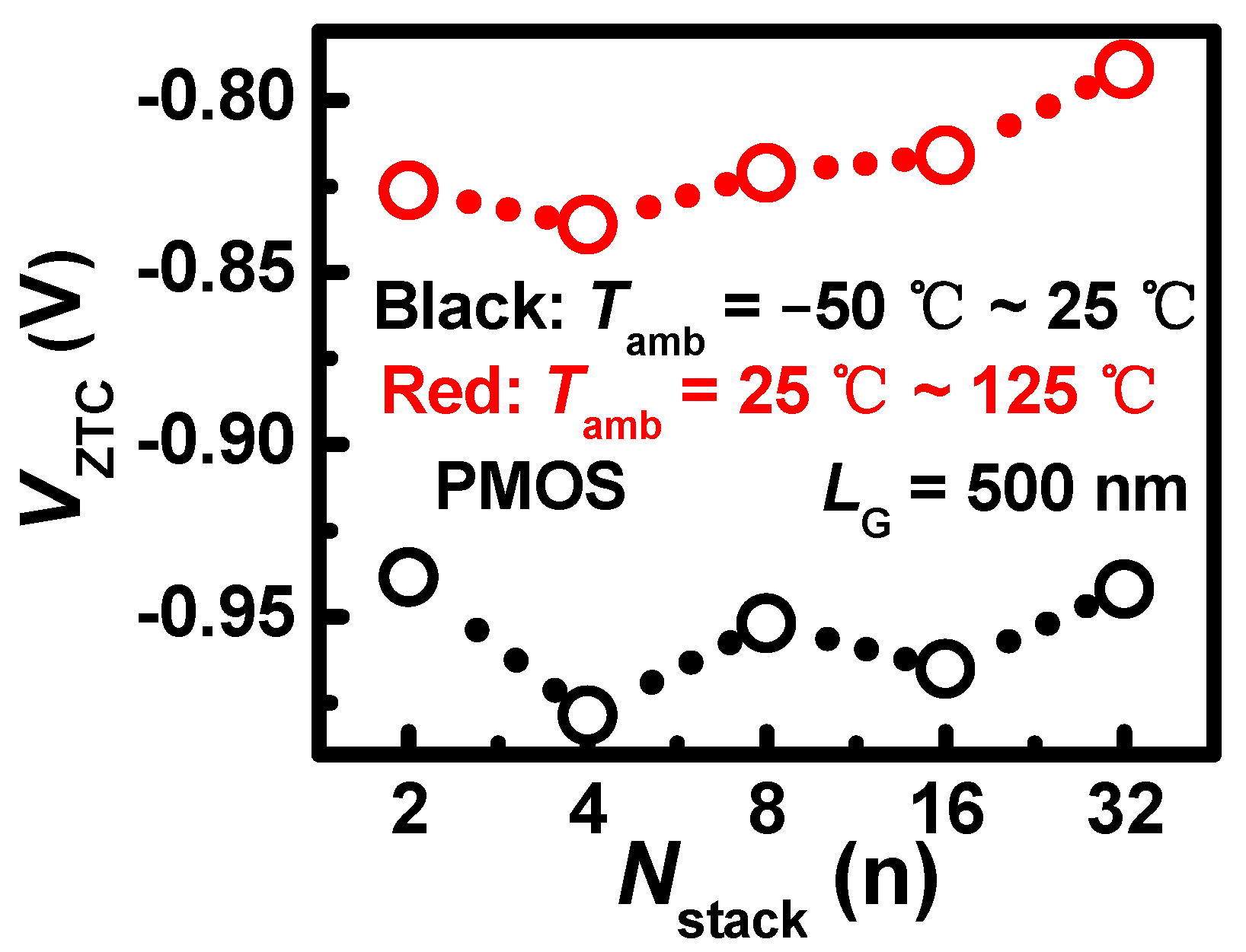
3.1. Electrothermal Performance of Different Numbers of Stacks under the Impact of Ambient Temperature

Since the measurement is dependent on ambient temperature (Tamb), the Tamb-dependent SHE in NSFETs is measured using the Agilent B1500 semiconductor parameter analyzer (Agilent Technologies, Santa Clara, CA, USA). The Tamb varies from −50 °C to 125 °C in a 25 °C step.
As shown in Figure 4, the transfer characteristic curves exhibit a variation in drain current (IDS) as the Tamb increases for NMOS and PMOS. The threshold voltages (Vths) are 300 mV and −300 mV at Tamb = 25 °C of room temperature (Trt) for NMOS and PMOS, respectively. The Vth is extracted using the constant current method. As the Tamb increases, the |Vth| decreases because the carrier concentration is positively correlated with the Tamb. In Figure 4a, the IDS of NMOS shows an increasing trend. Meanwhile, the IDS of PMOS also shows an increasing trend at a lower |VGS|. However, it exhibits a reverse temperature dependence at a larger |VGS|, as shown in Figure 4b. This is because the effect of the Vth reduction exceeds that of the mobility degradation in NMOS. However, the effect of the |Vth| reduction is inferior to that of the mobility degradation at a larger |VGS| in PMOS. Moreover, the IDS of PMOS is higher than that of NMOS at a larger |VGS|. The current degradation indicates that the higher current is more severely impacted by Tamb. In addition, it is found that the zero-temperature coefficient bias point (VZTC) occurs in PMOS, where the VZTC represents the bias voltage point that the IDS is independent of the Tamb [29]. In addition, there are two VZTC under Tamb = −50~25 °C range and Tamb = 25~125 °C range.
To explore the Tamb-dependent relation, Figure 5 shows that the IDS variations with different Nstacks under the impact of Tamb are extracted relative to the IDS at Tamb = −50 °C, and the gate overdrive voltage (Vov = VGSVth) is 0.43 V and −0.43 V for NMOS and PMOS, respectively. The IDS degradation of NMOS is lower than that of PMOS. At high Tamb, The NMOS with Nstack = 4 shows the largest IDS degradation, and other multiple stacks have minor differences. The devices with Nstack = 2 have the lowest IDS degradation at high Tamb in Figure 5a. PMOS shows a different trend when Nstack increases, as shown in Figure 5b. The PMOS with Nstack = 2 shows the largest IDS degradation, and other multiple stacks have minor differences. The PMOS with Nstack = 32 shows the lowest IDS degradation. The IDS variation in NMOS with Nstack = 4 and PMOS with Nstack = 2 may be induced by random structure irregularities.
To analyze the origin of the IDS variation, the temperature coefficients of IDS per stack (β) are extracted, as shown in Figure 6. Figure 6a shows that β in NMOS decreases in the negative direction under Tamb above Trt when Nstack is from 4 to 32. This is induced by the coupling mechanism with the impact of the SHE and Tamb. As the Nstack increases, the thermal crosstalk is enhanced in stacked nanosheets, where the thermal crosstalk is part of the SHE. The SHE can intensify phonon-electron scattering, and then counteract the partial effect of Tamb, resulting in reduced IDS degradation. In Section 3.3, the simulation results will further verify the speculation. The β in NMOS with Nstack = 2 is the lowest [Figure 6a]. This can be caused by difficult heat transport due to the smaller contact area between nanosheets and the S/D region, leading to severe thermal crosstalk. Meanwhile, the β under Tamb below 0 °C is basically larger than that under Tamb above Trt. This is because the impact of thermal crosstalk is weakened by enhanced heat transport ability.
Figure 6b shows that the β in PMOS is larger than that in NMOS. The carrier scattering intensifies by Tamb because the current density (JDS) in PMOS is larger than that in NMOS. The PMOS with Nstack = 2 exhibits the largest β. This reverse behavior is due to the highest JDS in PMOS with Nstack = 2 compared to NMOS. In addition, the difference of β when Nstack = 4~32 is small. This is because the difference in JDS of PMOS is small, and thus the difference in thermal crosstalk is relatively insignificant.
Then, the temperature coefficient of Vth (η) is extracted, as shown in Figure 7. The η in NMOS under Tamb above Trt rapidly decreases in the negative direction with Nstack first, and then the velocity of decrease gradually slows down [Figure 7a]. The η of NMOS with Nstack = 16 is the lowest. This is because the thermal crosstalk becomes severe; therefore, the impact of Tamb is mitigated. However, it increases when the Nstack grows to 32. This can be explained by the heat transport ability that the contact area between nanosheets and S/D regions gradually increases with Nstack, and then the enhanced thermal crosstalk effect is weakened. Therefore, the η with Nstack = 32 increases. The η in NMOS under Tamb below 0 °C rapidly decreases first, and then increases with Nstack = 16. The η in PMOS exhibits a similar trend compared with that in NMOS [Figure 7b]. However, the η value is larger.
The relation between the IDS variation and the η based on the temperature-dependent backscattering model is also further analyzed. In the temperature-dependent backscattering model [30,31], the IDS formula is defined using (1), and the linear relation of IDS and Tamb is given using (2). Finally, the analytic expression for α concerning temperature is given using (3):
I DS = W Q inj v th ( λ 0 / l 0 2 + λ 0 / l 0 )
Δ I DS / I DS = α ( T ( 50   ) )
α = ( 1 2 4 2 + λ 0 / l 0 ) / 298   K η V GS V th 0
In the equations, Qinj is the inverse layer density near the source region; νth is the thermal injection velocity at the thermal source; λ0 is the mean-free path; l0 is the critical distance when the carriers travel over a KT layer from the thermal source, where K and T are Boltzmann constant and temperature, respectively; and Vth0 is the threshold voltage at referenced temperature −50 °C. The α includes the backscattering coefficient term and the voltage-dependence term. In Figure 7, the η in PMOS is higher than that in NMOS significantly, and thus the second term of (3) becomes larger. This leads to a greater degradation of the IDS in PMOS compared to NMOS when Tamb increases, as shown in Figure 5.
As a special thermal phenomenon, the VZTC of PMOS is extracted in Figure 8. It is shown that the VZTC of PMOS decreases in the negative direction under Tamb above Trt when Nstack grows from 4 to 32. The result can be explained by the coupling mechanism with the impact of the SHE and Tamb. As the Nstack increases, the current variation comes to balance at lower |VGS| due to the effect of Vth and mobility. However, the VZTC under Tamb below Trt is 0.1 V higher than that under higher Tamb in the negative direction. This is because the SHE plays a lesser role in the case of Tamb below Trt. Therefore, the effect of Vth and mobility compensate at a higher VGS for the lower Tamb. The investigation of VZTC is useful to explore the working voltage in real applications.

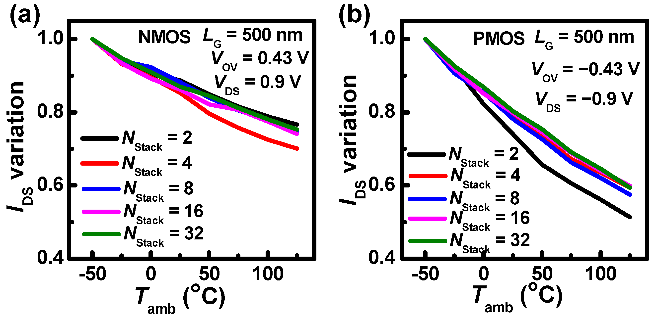
3.2. Electrothermal Performance of Different Gate Lengths with Different Nstacks under the Impact of Tamb

To explore the geometry effect, we further analyze the impact of gate lengths on electrical performance with different Nstacks, as shown in Figure 9. As LG increases, the degradation of IDS becomes severe. This can be explained by the temperature-dependent backscattering model.
As the LG increases, the channel potential decreases, and then l0 increases. Thus, the first term of (3) declines. This is an inverse result with the IDS degradation [Figure 9a]. Furthermore, the η is extracted, as shown in Figure 9b. The η increases in the negative direction as the LG increases at VDS = 0.9 V. Therefore, the IDS degradation is the result of both terms. At the same time, when the Nstack increases at VDS = 0.9 V, the devices with LG = 30, 40 nm show that the η decreases in the negative direction first, then, increases, similar to the trend of devices with LG = 500 nm. Remarkably, when VDS = 0.9 V, the slope of η with Nstack located in the 8 and 16 range is negative first, and then positive when the LG increases from 30 nm to 500 nm.
In addition, the IDS degradation in short gate length devices at VDS = 0.9 V is higher than that at VDS = 0.1 V. The difference gradually becomes larger with Tamb, and the device with LG = 30 nm has the largest difference. Figure 9b shows that the η increases in the negative direction as the VDS increases, and thus the second term of (3) becomes larger. Then, the λ0/l0 also increases with larger VDS, and the first term of (3) becomes larger. Finally, the IDS degradation is higher with larger VDS.

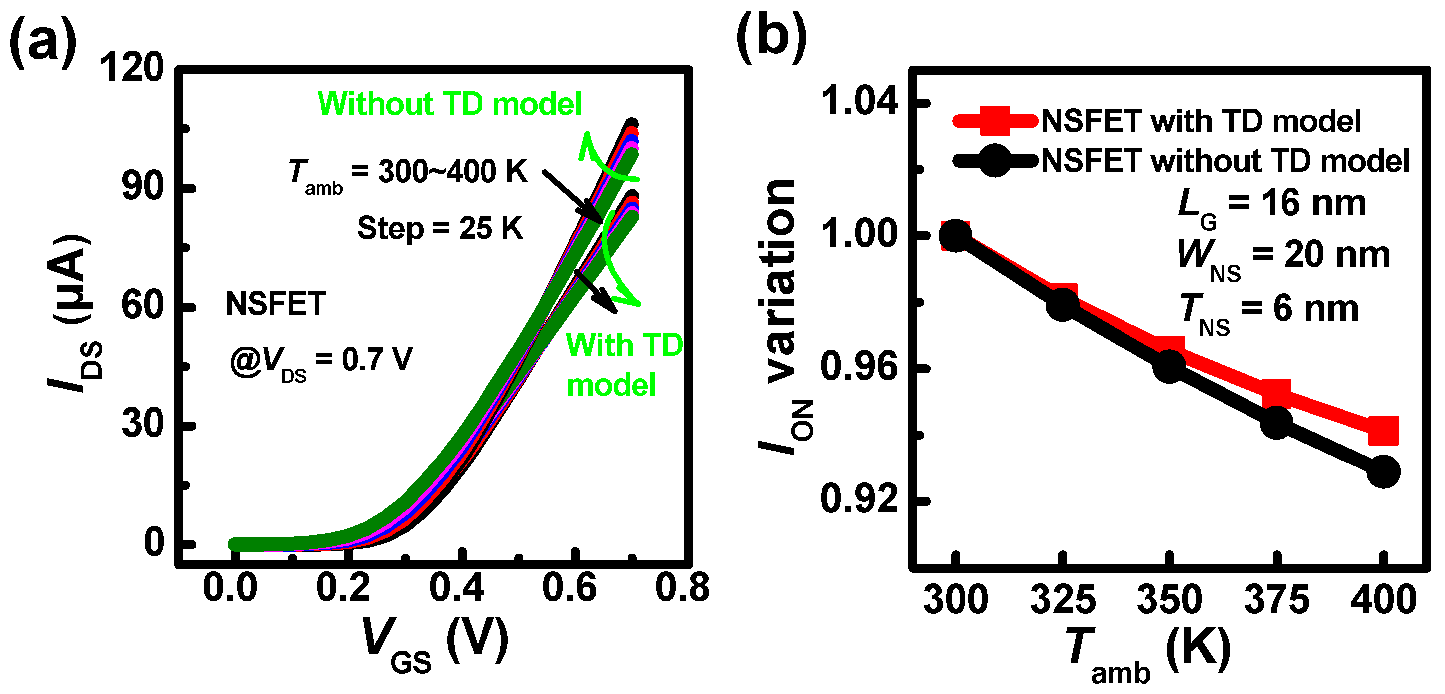
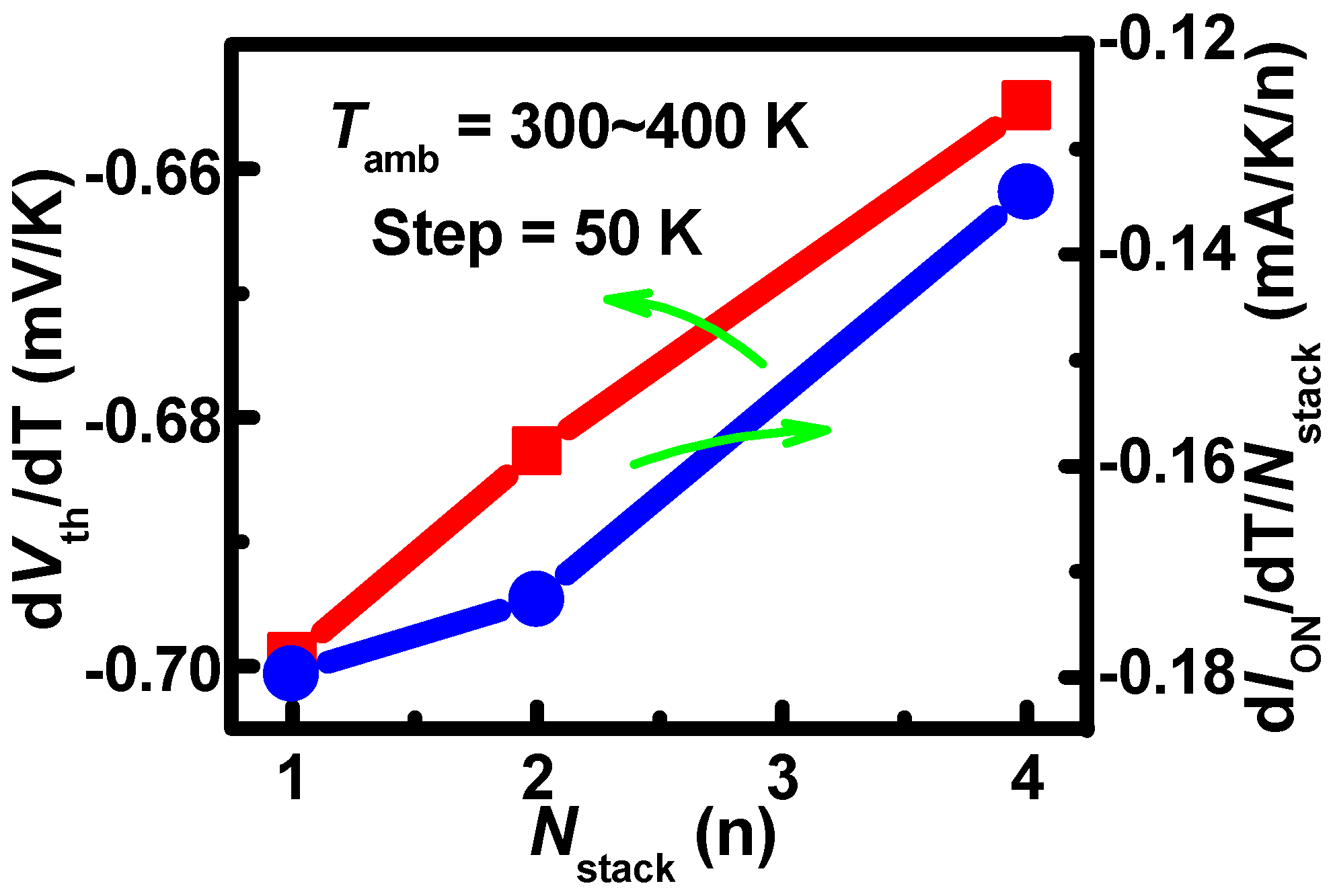
3.3. Simulation Verification

The coupling mechanism with the impact of the SHE and Tamb is verified using the simulation method. To clarify the SHE clearly, the 16 nm gate length devices are simulated. The simulated devices are 3 nm node NSFETs, referring to [1]. The electrothermal parameters are set according to [32], where the LG, WNS, and TNS are set to 16, 20, and 6 nm, respectively. The nanosheets adopt three layers of vertically stacked structure. All simulations are performed using Sentaurus TCAD tools [33]. The SHE is calculated with the thermodynamic model (TD model). Figure 10a shows that the IDS with the SHE is lower than that without the SHE at larger VGS. At VGS = VDS = 0.7 V, the on-state IDS (ION) degradation with the SHE is lower than that without the SHE as Tamb increases, as shown in Figure 10b. The results indicate that the SHE weakened the impact of Tamb. As the Nstack increases, the η declines in the negative direction as shown in Figure 11. At the same time, the β decreases with Nstack. This further verifies that the coupling heat counteracts the partial effect of Tamb.
To further investigate thermal characteristics, the thermal resistance (Rth) and the maximum lattice temperature rise (∆Tmax) with respect to Tamb are extracted. The Rth is defined using (4), where total heat includes Joule heat, Peltier heat, Tompson heat, and recombination heat [34].
Rth = ∆Tmax/total heat (K/μW)
The ∆Tmax and Rth in the devices with Nstack = 1 under Tamb = 300 K are 149 K and 2.59 K/μW, respectively, as shown in Figure 12. In Figure 12a, the ∆Tmax decreases with Tamb. However, the lattice temperature gradually increases. This explains why IDS with the SHE is lower at larger VGS [Figure 10a]. At the same time, the ∆Tmax increases when Nstack is from 1 to 2 first, and then has a minor variation when Nstack is from 2 to 4. This can be explained by the Rth variation with Nstack. In Figure 12b, the Rth per stack decreases with Tamb. This is because the ∆Tmax reduction ratio exceeds the ION degradation. Then, the Rth per stack increases when Nstack is from 1 to 2, and then the rising speed increases when Nstack is from 2 to 4. This is induced by the coupling effect. The rising Rth causes an increase in lattice temperature, leading to a decrease in current density, eventually, the ∆Tmax variation is low when Nstack is from 2 to 4 compared to that when Nstack is from 1 to 2. In addition, when the Tamb increases, the Rth decreases significantly in the devices with Nstack = 4 compared to that with Nstack = 1 and 2. This is because the coupling heat is more severe in the devices with Nstack = 4. These results verify that the SHE counteracts the partial effect of Tamb.

4. Conclusions

In this paper, the impact of Tamb on the SHE in NSFET with different Nstacks is investigated. The results show that the NMOS with Nstack = 2 has the lowest IDS degradation, and the IDS degradation of PMOS with Nstack = 32 is lower than that with Nstack = 2. The results show that the IDS degradation is lowest in the NMOS with Nstack = 2 and the PMOS with Nstack = 32 when the Tamb is at a high level. Due to the coupling mechanism with the impact of the SHE and Tamb, the η exhibits a decrease trend first, and then an increase trend with Nstack when the Tamb is higher than Trt. Remarkably, the VZTC of PMOS decreases with Nstack > 4 in the negative direction when Tamb is higher than Trt. Based on the backscattering theory, the IDS degradation ratio decreases when the LG becomes shorter. Meanwhile, the IDS degradation decreases at VDS = 0.1 V compared to that at VDS = 0.9 V in short gate length devices. Finally, the simulations verify that the SHE counteracts the partial effect of Tamb. The work explores the electrothermal characteristics when NSFETs with different Nstacks work under the impact of Tamb and provides design guidelines for real applications.

Author Contributions

Conceptualization, methodology, formal analysis and writing—original draft preparation, P.Z.; methodology, funding acquisition, formal analysis, supervision, review and editing, H.Y.; software, Z.W.; writing, review and editing, G.W.; investigation and resources, L.C. All authors have read and agreed to the published version of the manuscript.

Funding

This work was supported by the Strategic Priority Research Program of the Chinese Academy of Sciences (Grant No. XDA0330302); in part by the Joint Development Program of Semiconductor Technology Innovation Center (Beijing), Co.

Data Availability Statement

The data presented in this study are available on request from the corresponding author.

Acknowledgments

Thanks to the core CMOS program members of the Integrated Circuit Advanced Process Center (ICAC) at the Institute of Microelectronics of the Chinese Academy of Sciences, and the device fabrication on the ICAC pilot line.

Conflicts of Interest

Author Guilei Wang was employed by the company Process Integration, Beijing Superstring Academy of Memory Technology, China. The remaining authors declare that the research was conducted in the absence of any commercial or financial relationships that could be construed as a potential conflict of interest.

References

  1. International Roadmap for Devices and Systems (IRDS). 2020. Available online: https://irds.ieee.org/editions/2020 (accessed on 1 May 2023).
  2. Bae, G.; Bae, D.-I.; Kang, M.; Hwang, S.M.; Kim, S.S.; Seo, B.; Kwon, T.Y.; Lee, T.J.; Moon, C.; Choi, Y.M.; et al. 3nm GAA Technology Featuring Multi-Bridge-Channel FET for Low Power and High Performance Applications. In Proceedings of the 2018 IEEE International Electron Devices Meeting (IEDM), San Francisco, CA, USA, 1–5 December 2018; IEEE: Piscataway, NJ, USA, 2018; pp. 28.7.1–28.7.4. [Google Scholar]
  3. Loubet, N.; Hook, T.; Montanini, P.; Yeung, C.-W.; Kanakasabapathy, S.; Guillom, M.; Yamashita, T.; Zhang, J.; Miao, X.; Wang, J.; et al. Stacked Nanosheet Gate-All-around Transistor to Enable Scaling beyond FinFET. In Proceedings of the 2017 Symposium on VLSI Technology, Kyoto, Japan, 5–8 June 2017; IEEE: Piscataway, NJ, USA, 2017; pp. T230–T231. [Google Scholar]
  4. Myeong, I.; Song, I.; Kang, M.J.; Shin, H. Self-Heating and Electrothermal Properties of Advanced Sub-5-nm Node Nanoplate FET. IEEE Electron Device Lett. 2020, 41, 977–980. [Google Scholar] [CrossRef]
  5. Vermeersch, B.; Bury, E.; Xiang, Y.; Schuddinck, P.; Bhuwalka, K.K.; Hellings, G.; Ryckaert, J. Self-Heating in iN8–iN2 CMOS Logic Cells: Thermal Impact of Architecture (FinFET, Nanosheet, Forksheet and CFET) and Scaling Boosters. In Proceedings of the 2022 IEEE Symposium on VLSI Technology and Circuits (VLSI Technology and Circuits), Honolulu, HI, USA, 12–17 June 2022; IEEE: Piscataway, NJ, USA, 2022; pp. 371–372. [Google Scholar]
  6. Yoo, C.; Chang, J.; Seon, Y.; Kim, H.; Jeon, J. Analysis of Self-Heating Effects in Multi-Nanosheet FET Considering Bottom Isolation and Package Options. IEEE Trans. Electron Devices 2022, 69, 1524–1531. [Google Scholar] [CrossRef]
  7. Cai, L.; Chen, W.; Du, G.; Zhang, X.; Liu, X. Layout Design Correlated with Self-Heating Effect in Stacked Nanosheet Transistors. IEEE Trans. Electron Devices 2018, 65, 2647–2653. [Google Scholar] [CrossRef]
  8. Chung, C.-C.; Ye, H.-Y.; Lin, H.H.; Wan, W.K.; Yang, M.-T.; Liu, C.W. Self-Heating Induced Interchannel Vt Difference of Vertically Stacked Si Nanosheet Gate-All-Around MOSFETs. IEEE Electron Device Lett. 2019, 40, 1913–1916. [Google Scholar] [CrossRef]
  9. Shin, S.H.; Masuduzzaman, M.; Gu, J.J.; Wahab, M.A.; Conrad, N.; Si, M.; Ye, P.D.; Alam, M.A. Impact of Nanowire Variability on Performance and Reliability of Gate-All-around III-V MOSFETs. In Proceedings of the 2013 IEEE International Electron Devices Meeting, Washington, DC, USA, 9–11 December 2013; IEEE: Piscataway, NJ, USA, 2013; pp. 7.5.1–7.5.4. [Google Scholar]
  10. Myeong, I.; Son, D.; Kim, H.; Shin, H. Analysis of Self Heating Effect in DC/AC Mode in Multi-Channel GAA-Field Effect Transistor. IEEE Trans. Electron Devices 2019, 66, 4631–4637. [Google Scholar] [CrossRef]
  11. Venkateswarlu, S.; Nayak, K. Hetero-Interfacial Thermal Resistance Effects on Device Performance of Stacked Gate-All-Around Nanosheet FET. IEEE Trans. Electron Devices 2020, 67, 4493–4499. [Google Scholar] [CrossRef]
  12. Ahn, W.; Jiang, C.; Xu, J.; Alam, M.A. A New Framework of Physics-Based Compact Model Predicts Reliability of Self-Heated Modern ICs: FinFET, NWFET, NSHFET Comparison. In Proceedings of the 2017 IEEE International Electron Devices Meeting (IEDM), San Francisco, CA, USA, 2–6 December 2017; IEEE: Piscataway, NJ, USA, 2017; pp. 13.6.1–13.6.4. [Google Scholar]
  13. Jiang, H.; Shin, S.; Liu, X.; Zhang, X.; Alam, M.A. The Impact of Self-Heating on HCI Reliability in High-Performance Digital Circuits. IEEE Electron Device Lett. 2017, 38, 430–433. [Google Scholar] [CrossRef]
  14. Qu, Y.; Lin, X.; Li, J.; Cheng, R.; Yu, X.; Zheng, Z.; Lu, J.; Chen, B.; Zhao, Y. Ultra Fast (<1 Ns) Electrical Characterization of Self-Heating Effect and Its Impact on Hot Carrier Injection in 14nm FinFETs. In Proceedings of the 2017 IEEE International Electron Devices Meeting (IEDM), San Francisco, CA, USA, 2–6 December 2017; IEEE: Piscataway, NJ, USA, 2017; pp. 39.2.1–39.2.4. [Google Scholar]
  15. Zhao, Y.; Qu, Y. Impact of Self-Heating Effect on Transistor Characterization and Reliability Issues in Sub-10 nm Technology Nodes. IEEE J. Electron Devices Soc. 2019, 7, 829–836. [Google Scholar] [CrossRef]
  16. Jiang, H.; Xu, N.; Chen, B.; Zeng, L.; He, Y.; Du, G.; Liu, X.; Zhang, X. Experimental Investigation of Self Heating Effect (SHE) in Multiple-Fin SOI FinFETs. Semicond. Sci. Technol. 2014, 29, 115021. [Google Scholar] [CrossRef]
  17. Wang, R.; Zhuge, J.; Liu, C.; Huang, R.; Kim, D.-W.; Park, D.; Wang, Y. Experimental Study on Quasi-Ballistic Transport in Silicon Nanowire Transistors and the Impact of Self-Heating Effects. In Proceedings of the 2008 IEEE International Electron Devices Meeting, San Francisco, CA, USA, 15–17 December 2008; IEEE: Piscataway, NJ, USA, 2008; pp. 1–4. [Google Scholar]
  18. Jain, I.; Gupta, A.; Hook, T.B.; Dixit, A. Modeling of Effective Thermal Resistance in Sub-14-Nm Stacked Nanowire and FinFETs. IEEE Trans. Electron Devices 2018, 65, 4238–4244. [Google Scholar] [CrossRef]
  19. Liu, R.; Li, X.; Sun, Y.; Shi, Y. A Vertical Combo Spacer to Optimize Electrothermal Characteristics of 7-Nm Nanosheet Gate-All-Around Transistor. IEEE Trans. Electron Devices 2020, 67, 2249–2254. [Google Scholar] [CrossRef]
  20. Jang, D.; Bury, E.; Ritzenthaler, R.; Bardon, M.G.; Chiarella, T.; Miyaguchi, K.; Raghavan, P.; Mocuta, A.; Groeseneken, G.; Mercha, A.; et al. Self-Heating on Bulk FinFET from 14nm down to 7nm Node. In Proceedings of the 2015 IEEE International Electron Devices Meeting (IEDM), Washington, DC, USA, 7–9 December 2015; IEEE: Piscataway, NJ, USA, 2015; pp. 11.6.1–11.6.4. [Google Scholar]
  21. Rodriguez, N.; Navarro, C.; Andrieu, F.; Faynot, O.; Gamiz, F.; Cristoloveanu, S. Self-Heating Effects in Ultrathin FD SOI Transistors. In Proceedings of the IEEE 2011 International SOI Conference, Tempe, AZ, USA, 3–6 October 2011; IEEE: Piscataway, NJ, USA, 2011; pp. 1–2. [Google Scholar]
  22. Tu, R.H.; Wann, C.; King, J.C.; Ko, P.K.; Hu, C. An AC Conductance Technique for Measuring Self-Heating in SOI MOSFET’s. IEEE Electron Device Lett. 1995, 16, 67–69. [Google Scholar] [CrossRef]
  23. Venkateswarlu, S.; Sudarsanan, A.; Singh, S.G.; Nayak, K. Ambient Temperature-Induced Device Self-Heating Effects on Multi-Fin Si n-FinFET Performance. IEEE Trans. Electron Devices 2018, 65, 2721–2728. [Google Scholar] [CrossRef]
  24. Kumar, N.; Kaushik, P.K.; Kumar, S.; Gupta, A.; Singh, P. Thermal Conductivity Model to Analyze the Thermal Implications in Nanowire FETs. IEEE Trans. Electron Devices 2022, 69, 6388–6393. [Google Scholar] [CrossRef]
  25. Takahashi, T.; Beppu, N.; Chen, K.; Oda, S.; Uchida, K. Thermal-Aware Device Design of Nanoscale Bulk/SOI FinFETs: Suppression of Operation Temperature and Its Variability. In Proceedings of the 2011 International Electron Devices Meeting, Washington, DC, USA, 5–7 December 2011; IEEE: Piscataway, NJ, USA, 2011; pp. 34.6.1–34.6.4. [Google Scholar]
  26. Venkateswarlu, S.; Nayak, K. Ambient Temperature-Induced Device Self-Heating Effects on Multi-Fin Si CMOS Logic Circuit Performance in N-14 to N-7 Scaled Technologies. IEEE Trans. Electron Devices 2020, 67, 1530–1536. [Google Scholar] [CrossRef]
  27. Mertens, H.; Ritzenthaler, R.; Hikavyy, A.; Kim, M.S.; Tao, Z.; Wostyn, K.; Chew, S.A.; De Keersgieter, A.; Mannaert, G.; Rosseel, E.; et al. Gate-All-around MOSFETs Based on Vertically Stacked Horizontal Si Nanowires in a Replacement Metal Gate Process on Bulk Si Substrates. In Proceedings of the 2016 IEEE Symposium on VLSI Technology, Honolulu, HI, USA, 14–16 June 2016; IEEE: Piscataway, NJ, USA, 2016; pp. 1–2. [Google Scholar]
  28. Zhang, Q.; Gu, J.; Xu, R.; Cao, L.; Li, J.; Wu, Z.; Wang, G.; Yao, J.; Zhang, Z.; Xiang, J.; et al. Optimization of Structure and Electrical Characteristics for Four-Layer Vertically-Stacked Horizontal Gate-All-Around Si Nanosheets Devices. Nanomaterials 2021, 11, 646. [Google Scholar] [CrossRef] [PubMed]
  29. Triantopoulos, K.; Casse, M.; Brunet, L.; Batude, P.; Fenouillet-Beranger, C.; Reimbold, G.; Ghibaudo, G. Self-Heating Assessment and Cold Current Extraction in FDSOI MOSFETs. In Proceedings of the 2017 IEEE SOI-3D-Subthreshold Microelectronics Technology Unified Conference (S3S), Burlingame, CA, USA, 16–19 October 2017; IEEE: Piscataway, NJ, USA, 2017; pp. 1–3. [Google Scholar]
  30. Lundstrom, M. Elementary Scattering Theory of the Si MOSFET. IEEE Electron Device Lett. 1997, 18, 361–363. [Google Scholar] [CrossRef]
  31. Chen, M.-J.; Huang, H.-T.; Huang, K.-C.; Chen, P.-N.; Chang, C.-S.; Diaz, C.H. Temperature Dependent Channel Backscattering Coefficients in Nanoscale MOSFETs. In Proceedings of the Digest. International Electron Devices Meeting, San Francisco, CA, USA, 8–11 December 2002; IEEE: Piscataway, NJ, USA, 2002; pp. 39–42. [Google Scholar]
  32. Zhao, P.; Cao, L.; Zhang, F.; Xu, H.; Gan, W.; Zhang, Q.; Zhang, Z.; Yao, J.; Tian, G.; Luo, K.; et al. Investigation on Dependency of Thermal Characteristics on Gate/Drain Bias Voltages in Stacked Nanosheet Transistors. Microelectron. J. 2023, 141, 105970. [Google Scholar] [CrossRef]
  33. Sentaurus Device User Guide, Version P-2019.03; Synopsys: Mountain View, CA, USA, 2019.
  34. Kang, S.J.; Kim, J.H.; Song, Y.S.; Go, S.; Kim, S. Investigation of Self-Heating Effects in Vertically Stacked GAA MOSFET with Wrap-Around Contact. IEEE Trans. Electron Devices 2022, 69, 910–914. [Google Scholar] [CrossRef]
Figure 1. (a) Process flow of GAA NSFETs adopting the gate last process. (b) Schematic of the NSFET with multiple lateral stacks along the nanosheet width direction.
Nanomaterials 13 02971 g001
Figure 2. The TEM image of GAA NSFETs in this work. The nanosheets are separated from each other.
Nanomaterials 13 02971 g002
Figure 3. The EDS images of NSFETs in this work. The top figures illustrate W, Si, and O elements. The middle figures illustrate Hf, Ti, and N elements. The bottom figures illustrate Al, Ta, and Ge elements. Ge has been removed completely.
Nanomaterials 13 02971 g003
Figure 4. Experimental temperature dependence of transfer characteristics at LG = 500 nm, Nstack = 2, (a) VDS = 0.9 V for NMOS and (b) VDS = −0.9 V for PMOS. It shows two VZTC under Tamb = −50~25 °C range and Tamb = 25~125 °C range.
Nanomaterials 13 02971 g004
Figure 5. (a) IDS variations of NMOS with different Nstacks under the impact of Tamb relative to the IDS at Tamb = −50 °C, (b) IDS variations of PMOS with different Nstacks under the impact of Tamb relative to the IDS at Tamb = −50 °C.
Nanomaterials 13 02971 g005
Figure 6. LG = 500 nm, (a) VDS = 0.9 V, Vov = 0.59 V, the temperature coefficients of IDS per stack in NMOS, (b) VDS = −0.9 V, Vov = −0.59 V, the temperature coefficients of IDS per stack in PMOS under different Tamb ranges.
Nanomaterials 13 02971 g006
Figure 7. LG = 500 nm, the temperature coefficients of Vth (η) with different Nstacks in (a) NMOS and (b) PMOS under different Tamb ranges.
Nanomaterials 13 02971 g007
Figure 8. LG = 500 nm, the VZTC of PMOS with different Nstack under Tamb = −50–25 °C range and Tamb = 25–125 °C range.
Nanomaterials 13 02971 g008
Figure 9. (a) IDS variations with different gate lengths under the impact of Tamb relative to the IDS at Tamb = −50 °C. (b) The temperature coefficients of Vth with different gate lengths when the Nstack increases.
Nanomaterials 13 02971 g009
Figure 10. (a) The transfer characteristics of NSFET (Nstack = 1) with/without the SHE as the Tamb increases from 300 K to 400 K, (b) IDS variations relative to the IDS at Tamb = 300 K with/without the SHE when VGS = VDS = 0.7 V.
Nanomaterials 13 02971 g010
Figure 11. The temperature coefficients of Vth and the temperature coefficients of IDS per stack with different Nstacks.
Nanomaterials 13 02971 g011
Figure 12. When VGS = VDS = 0.7 V, (a) ∆Tmax and (b) Rth variations relative to the devices with Nstack = 1 under Tamb = 300 K.
Nanomaterials 13 02971 g012
Disclaimer/Publisher’s Note: The statements, opinions and data contained in all publications are solely those of the individual author(s) and contributor(s) and not of MDPI and/or the editor(s). MDPI and/or the editor(s) disclaim responsibility for any injury to people or property resulting from any ideas, methods, instructions or products referred to in the content.

