Direct Imprinting of Large-Area Metallic Photonic Lattices for Infrared Polarization Filters with Broadband Tunability
Abstract
:1. Introduction
2. Materials and Methods
2.1. Materials
2.2. Fabrication Processes
- (i)
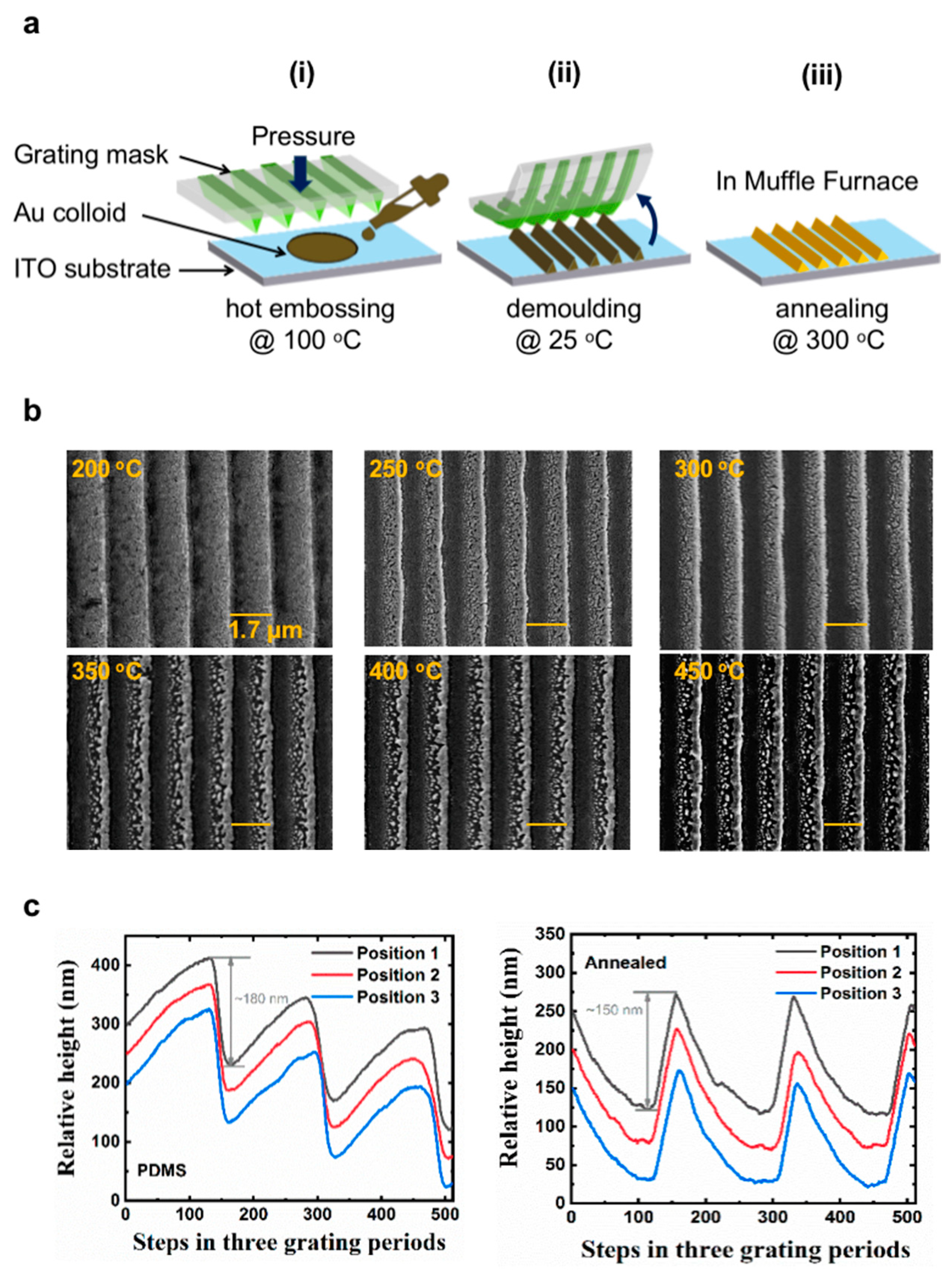
- Hot embossing: the Au nanoparticle colloidal (10 μL) is drop-cast on an ITO (indium tin oxide) substrate on a hot plate at 100 °C. A PDMS mold is pressed on the Au nanoparticle colloid with a pressure of 0.25 kg/cm2 before the colloid dries. The thickness of the grating can be tuned by altering the pressure, the volume, and the concentration of the Au nanoparticle colloidal.
- (ii)
- Demolding: after hot embossing, the sample is removed from the hot plate to room temperature. When the temperature cools sufficiently (within about 1 min), the PDMS stamp can be demolded from the solidified Au nanoparticle colloid. The surface energy of ITO is higher than the PDMS stamp, and thus the Au nanoparticle colloid will stay on the ITO surface during demolding. The grating is therefore copied from the PDMS stamp to the solidified Au nanoparticle colloid, which will show up on top of the ITO substrate.
- (iii)
- Annealing: the solidified Au nanoparticle colloid is annealed in a Muffle Furnace at 300 °C for 10 min to let the Au nanoparticle fully melt and aggregate. The temperature of annealing is important; when the temperature is too low (200 °C), the nanoparticles cannot be melted: note that the 200 °C image in Figure 1b is similar to that of the sample before annealing (Figure S2). Once the temperature reaches 250 °C, the Au nanoparticles melt. The SEM image shows confined structures because, after the phase transition, melted Au nanoparticles can flow within a limited space to meet other melted nanoparticles. Thus, aggregates form and solidify. Continuous Au wires can be realized via the optimization of parameters, such as embossing pressure, colloid concentration, etc. However, if the annealing temperature is too high, the agglomerate nanoparticles formed can further be melted at this temperature, which means they may flow to meet other agglomerate nanoparticles. This results in the formation of large, solidified Au-bulk, leaving space in the grooves, as illustrated in Figure 1b’s 350 °C, 400 °C, and 450 °C cases. More parameter-dependent structures are illustrated in the supporting information in Figures S3–S6.
3. Results and Discussion
3.1. Structure Characterization
3.2. Measurements of Polarization Selectivity and Angle Tuning Properties
3.2.1. Broadband Polarization Selectivity
3.2.2. Broadband Angle-Tuning Properties
3.3. Metallic Photonic Lattices with Different Structures
4. Conclusions
Supplementary Materials
Author Contributions
Funding
Institutional Review Board Statement
Informed Consent Statement
Data Availability Statement
Conflicts of Interest
References
- Zeng, B.; Gao, Y.; Bartoli, F.J. Ultrathin Nanostructured Metals for Highly Transmissive Plasmonic Subtractive Color Filters. Sci. Rep. 2013, 3, 2840. [Google Scholar] [CrossRef] [PubMed]
- Neutens, P.; Lagae, L.; Borghs, G.; Dorpe, P.V. Plasmon FIlters and metal-insulator-metal waveguides. Opt. Express 2012, 20, 3408–3423. [Google Scholar] [CrossRef] [PubMed]
- Wang, Y.; Zhang, X. Ultrafast Optical Switching Based on Mutually Enhanced Resonance Modes in Gold Nanowire Gratings. Nanoscale 2019, 11, 17807–17814. [Google Scholar] [CrossRef] [PubMed]
- Gao, H.; Henzie, J.; Odom, T.W. Direct Evidence for Surface Plasmon-Mediated Enhanced Light Transmission through Metallic Nanohole Arrays. Nano Lett. 2006, 6, 2104–2108. [Google Scholar] [CrossRef] [PubMed]
- Tvingstedt, K.; Persson, N.-K.; Inganas, O.; Rahachou, A.; Zozoulenko, I.V. Surface Plasmon Increase Absorption in Polymer Photovoltaic Cells. Appl. Phys. Lett. 2007, 91, 113514. [Google Scholar] [CrossRef]
- Atwater, H.A.; Polman, A. Plasmonics for Improved Photovoltaic Devices. Nat. Mater. 2010, 9, 205–213. [Google Scholar] [CrossRef]
- Gan, Q.; Bartoli, F.J.; Kafafi, Z.H. Plasmonic-Enhanced Organic Photovoltaics: Breaking the 10% Efficiency Barrier. Adv. Mater. 2013, 25, 2385–2396. [Google Scholar] [CrossRef]
- Xiang, J.; Wang, Y.; Wu, Y.; Fang, H.; Shui, L.; Liu, Z.; Ding, T. Ordered Hierarchical Ag Nanostructures as Surface-Enhanced Raman Scattering Platforms for (Bio)Chemical Sensing and Pollutant Monitoring. ACS Appl. Nano Mater. 2021, 4, 11644–11650. [Google Scholar] [CrossRef]
- Zhang, X.; Feng, S.; Zhang, J.; Zhai, T.; Liu, H.; Pang, Z. Sensors Based on Plasmonic-Photonic Coupling in Metallic Photonic Crystals. Sensors 2012, 12, 12082–12097. [Google Scholar] [CrossRef]
- Zhang, X.; Liu, H.; Tian, J.; Song, Y.; Wang, L. Band-Selective Optical Polarizer Based on Gold-Nanowire Plasmonic Diffraction Gratings. Nano Lett. 2008, 8, 2653–2658. [Google Scholar] [CrossRef]
- Shi, S.; Lu, N.; Lu, Y.; Wang, Y.; Qi, D.; Xu, H.; Chi, L. Fabrication of Periodic Metal Nanowires with Microscale Mold by Nanoimprint Lithography. ACS Appl. Mater. Interfaces 2011, 3, 4174–4179. [Google Scholar] [CrossRef] [PubMed]
- Grande, M.; Vincenti, M.A.; Stomeo, T.; Morea, G.; Marani, R.; Marrocco, V.; Petruzzelli, V.; D’Orazio, A.; Cingolani, R.; De Vittorio, M.; et al. Experimental Demonstration of a Novel Bio-sensing Platform via Plasmonic Band Gap Formation in Gold Nano-patch Arrays. Opt. Express 2011, 19, 21385. [Google Scholar] [CrossRef] [PubMed]
- Grande, M.; Marani, R.; Portincasa, F.; Morea, G.; Petruzzelli, V.; D’Orazio, A.; Marrocco, V.; De Ceglia, D.; Vincenti, M.A. Asymmetric Plasmonic Grating for Optical Sensing of Thin Layers of Organic Materials. Sensors Actuators, B Chem. 2011, 160, 1056–1062. [Google Scholar] [CrossRef]
- Ibbotson, L.A.; Demetriadou, A.; Croxall, S.; Hess, O.; Baumberg, J.J. Optical Nano-Woodpiles: Large-Area Metallic Photonic Crystals and Metamaterials. Sci. Rep. 2015, 5, 8313. [Google Scholar] [CrossRef] [PubMed]
- Garcia, J.A.; Hrelescu, C.; Zhang, X.; Grosso, D.; Abbarchi, M.; Bradley, A.L. Quasi-Guided Modes in Titanium Dioxide Arrays Fabricated via Soft Nanoimprint Lithography. ACS Appl. Mater. Interfaces 2021, 13, 47860–47870. [Google Scholar] [CrossRef]
- Bruchhaus, L.; Mazarov, P.; Bischoff, L.; Gierak, J.; Wieck, A.D.; Hövel, H. Comparison of Technologies for Nano Device Prototyping with a Special Focus on Ion Beams: A Review. Appl. Phys. Rev. 2017, 4, 011302. [Google Scholar] [CrossRef]
- Dan, V.; Dmitruk, M.; Indutnyi, I.; Mamykin, S.; Myn, V.; Lukaniuk, M. Fabrication of Periodic Plasmonic Structures Using Interference Lithography and Chalcogenide Photoresist. Nanoscale Res. Lett. 2015, 10, 1–8. [Google Scholar] [CrossRef]
- Guo, L.J. Nanoimprint Lithography: Methods and Material Requirements. Adv. Mater. 2007, 19, 495–513. [Google Scholar] [CrossRef]
- Kothari, R.; Beaulieu, M.R.; Hendricks, N.R.; Li, S.; Watkins, J.J. Direct Patterning of Robust One-Dimensional, Two-Dimensional, and Three-Dimensional Crystalline Metal Oxide Nanostructures Using Imprint Lithography and Nanoparticle Dispersion Inks. Chem. Mater. 2017, 29, 3908–3918. [Google Scholar] [CrossRef]
- Zhai, T.; Zhang, X.; Pang, Z.; Dou, F. Direct Writing of Polymer Lasers Using Interference Ablation. Adv. Mater. 2011, 23, 1860–1864. [Google Scholar] [CrossRef]
- Chou, S.Y.; Krauss, P.R.; Renstrom, P.J. Imprint of Sub-25 Nm Vias and Trenches in Polymers. Appl. Phys. Lett. 1995, 67, 3114. [Google Scholar] [CrossRef]
- Mcdonald, J.C.; Duffy, D.C.; Anderson, J.R.; Chiu, D.T. Review General Fabrication of Microfluidic Systems in Poly (Dimethylsiloxane). Electrophoresis 2000, 21, 27–40. [Google Scholar] [CrossRef]
- Hu, Y.; Li, G.; Cai, J.; Zhang, C.; Li, J.; Chu, J.; Huang, W. Facile Fabrication of Functional PDMS Surfaces with Tunable Wettablity and High Adhesive Force via Femtosecond Laser Textured Templating. AIP Adv. 2014, 4, 127141. [Google Scholar] [CrossRef]
- Nanoparticles, S.G.; Zhang, X.; Sun, B.; Friend, R.H. Metallic Photonic Crystals Based On. Nano Lett. 2006, 6, 651–655. [Google Scholar]
- Zhang, X.; Liu, H.; Feng, S. Solution-Processible Fabrication of Large-Area Patterned and Unpatterned Gold Nanostructures. Nanotechnology 2009, 20, 425303. [Google Scholar] [CrossRef] [PubMed]
- Modaresialam, M.; Chehadi, Z.; Bottein, T.; Abbarchi, M.; Grosso, D. Nanoimprint Lithography Processing of Inorganic-Based Materials. Chem. Mater. 2021, 33, 5464–5482. [Google Scholar] [CrossRef]
- Halas, N.J.; Lal, S.; Chang, W.; Link, S.; Nordlander, P. Halas_ChemRev_2011_Plasmons in Strongly Coupled Metallic Nanostructures.Pdf. Chem. Rev. 2011, 111, 3913–3961. [Google Scholar] [CrossRef]
- Liu, F.; Zhang, X. Fano Coupling between Rayleigh Anomaly and Localized Surface Plasmon Resonance for Sensor Applications. Biosens. Bioelectron. 2015, 68, 719–725. [Google Scholar] [CrossRef]
- Shah, Y.D.; Grant, J.; Hao, D.; Kenney, M.; Pusino, V.; Cumming, D.R.S. Ultra-Narrow Line Width Polarization-Insensitive Filter Using a Symmetry-Breaking Selective Plasmonic Metasurface. ACS Photonics 2018, 5, 663–669. [Google Scholar] [CrossRef]
- Ng, R.C.; Garcia, J.C.; Greer, J.R.; Fountaine, K.T. Polarization-Independent, Narrow-band, Near-IR Spectral Filters via Guided Mode Resonances in Ultrathin a-Si Nanopillar Arrays. ACS Photonics 2019, 6, 265–271. [Google Scholar] [CrossRef]
- Wang, R.; Wang, R.; Gong, Q.H.; Chen, J.J.; Chen, J.J.; Chen, J.J. Extra-Narrowband Metallic Filters with an Ultrathin Single-Layer Metallic Grating. Chin. Phys. B 2020, 29, 064215. [Google Scholar] [CrossRef]
- Barrow, M.; Phillips, J. Mid-Wave Infrared Transmittance Filters in Suspended GaAs Subwavelength Gratings. Appl. Phys. Lett. 2021, 119, 031103. [Google Scholar] [CrossRef]
- Shi, X.; Chen, C.; Liu, S.; Li, G. Nonvolatile, Reconfigurable and Narrow-band Mid-Infrared Filter Based on Surface Lattice Resonance in Phase-Change Ge2sb2te5. Nanomaterials 2020, 10, 2530. [Google Scholar] [CrossRef]
- Chen, Y.G.; Kao, T.S.; Ng, B.; Li, X.; Luo, X.G.; Luk’yanchuk, B.; Maier, S.A.; Hong, M.H. Hybrid Phase-Change Plasmonic Crystals for Active Tuning of Lattice Resonances. Opt. Express 2013, 21, 13691. [Google Scholar] [CrossRef] [PubMed]
- Li, H.J.; Wang, L.L.; Sun, B.; Huang, Z.R.; Zhai, X. Controlling Mid-Infrared Surface Plasmon Polaritons in the Parallel Graphene Pair. Appl. Phys. Express 2014, 7, 125101. [Google Scholar] [CrossRef]
- Ko, Y.H.; Lee, K.J.; Simlan, F.A.; Gupta, N.; Magnusson, R. Dual Angular Tunability of 2D Ge/ZnSe Notch Filters: Analysis, Experiments, Physics. Adv. Opt. Mater. 2022, 11, 2202390. [Google Scholar] [CrossRef]
- Mao, H.; Dong, X.; Liu, Y.; Silva, K.K.M.B.D.; Faraone, L. A Suspended Metamaterial Mirror for Hyperspectral Shortwave Infrared Fabry-Perot Filters. J. Microelectromechanical Syst. 2022, 31, 644–652. [Google Scholar] [CrossRef]


| Incident Angle (°) | Center Wavelength (nm) | Cutoff Wavelength (nm) | Filter Ratio (%) | Bandwidth (FWHM) (nm) |
|---|---|---|---|---|
| 0 | 1893 | 1721 | 88.6 | 258 ± 2 |
| 4 | 2006 | 1862 | 50.7 | 243 ± 2 |
| 8 | 2113 | 1994 | 61.4 | 286 ± 2 |
| 12 | 2210 | 2100 | 61.6 | 224 ± 2 |
| 16 | 2314 | 2206 | 62.3 | / |
| Angle-Tuning (°) | Center Wavelength (nm) | Filter Ratio (%) | Bandwidth (FWHM) (nm) | Reported Polarization Filters |
|---|---|---|---|---|
| yes | 1893 | 88.6 | 258 | This work |
| no | 1640 | 44 | 79 | [29] |
| no | 1540 | 90 | 20 | [30] |
| no | 900 | 80 | 3 | [31] |
| no | 6310 | 57 | 113 | [32] |
| no | 3179 | 72.6 | 162 | [33] |
| no | 1890 | 83 | 111 | [34] |
| no | 8480 | / | 237 | [35] |
| yes | 9680–10,970 | >90 | 180–580 | [36] |
| no | 2458 | 80 | 4 | [37] |
Disclaimer/Publisher’s Note: The statements, opinions and data contained in all publications are solely those of the individual author(s) and contributor(s) and not of MDPI and/or the editor(s). MDPI and/or the editor(s) disclaim responsibility for any injury to people or property resulting from any ideas, methods, instructions or products referred to in the content. |
© 2023 by the authors. Licensee MDPI, Basel, Switzerland. This article is an open access article distributed under the terms and conditions of the Creative Commons Attribution (CC BY) license (https://creativecommons.org/licenses/by/4.0/).
Share and Cite
Dou, F.; Peng, C.; Zou, M.; Zhang, X. Direct Imprinting of Large-Area Metallic Photonic Lattices for Infrared Polarization Filters with Broadband Tunability. Nanomaterials 2023, 13, 1022. https://doi.org/10.3390/nano13061022
Dou F, Peng C, Zou M, Zhang X. Direct Imprinting of Large-Area Metallic Photonic Lattices for Infrared Polarization Filters with Broadband Tunability. Nanomaterials. 2023; 13(6):1022. https://doi.org/10.3390/nano13061022
Chicago/Turabian StyleDou, Fei, Chen Peng, Miaomiao Zou, and Xinping Zhang. 2023. "Direct Imprinting of Large-Area Metallic Photonic Lattices for Infrared Polarization Filters with Broadband Tunability" Nanomaterials 13, no. 6: 1022. https://doi.org/10.3390/nano13061022
APA StyleDou, F., Peng, C., Zou, M., & Zhang, X. (2023). Direct Imprinting of Large-Area Metallic Photonic Lattices for Infrared Polarization Filters with Broadband Tunability. Nanomaterials, 13(6), 1022. https://doi.org/10.3390/nano13061022


