
Hollow Spherical Pd/CdS/NiS with Carrier Spatial Separation for Photocatalytic Hydrogen Generation
Abstract
:1. Introduction
2. Experimental Details
2.1. Materials
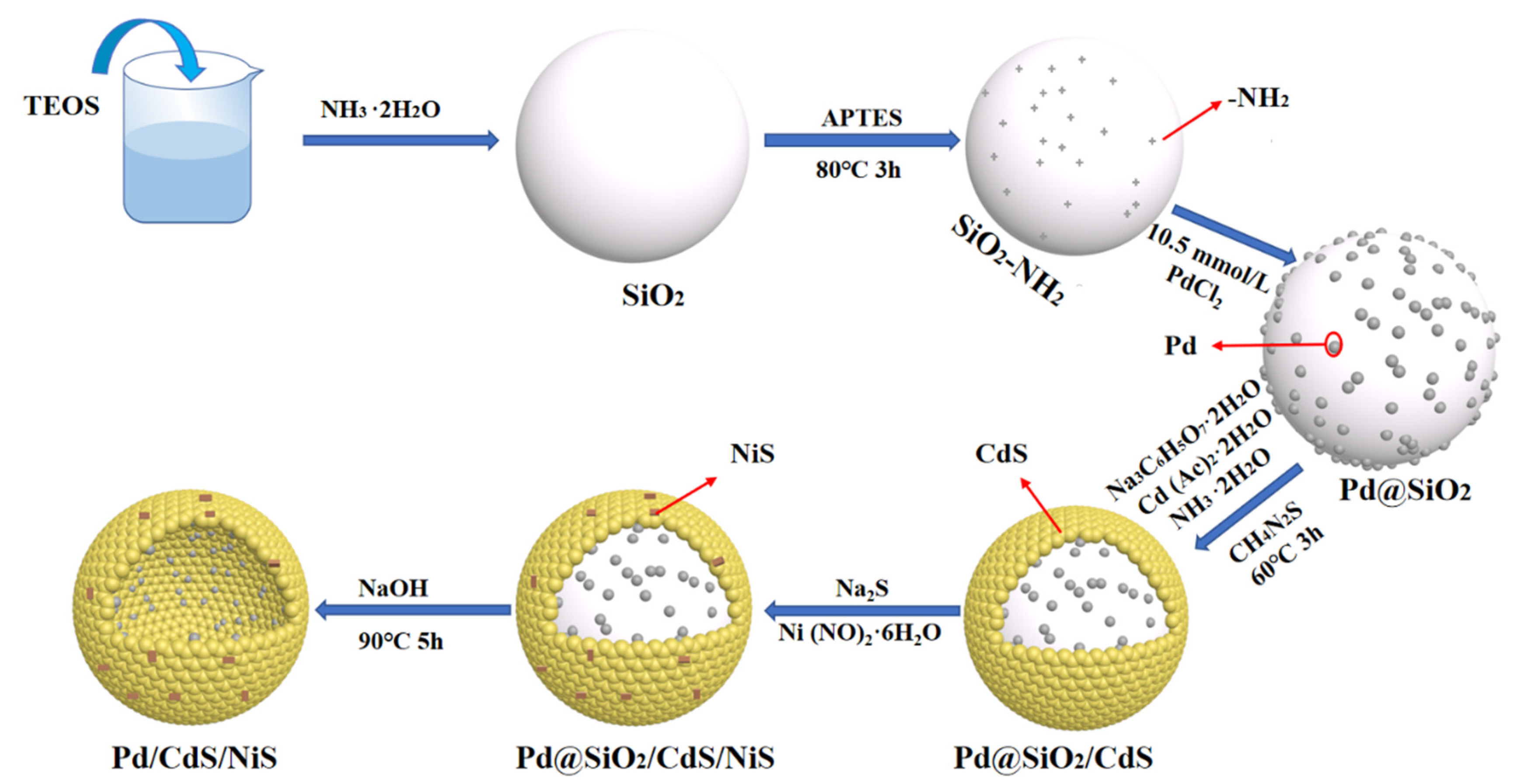
2.2. Synthesis
2.3. Characterization
2.4. Photocatalytic Activity
3. Results and Discussion
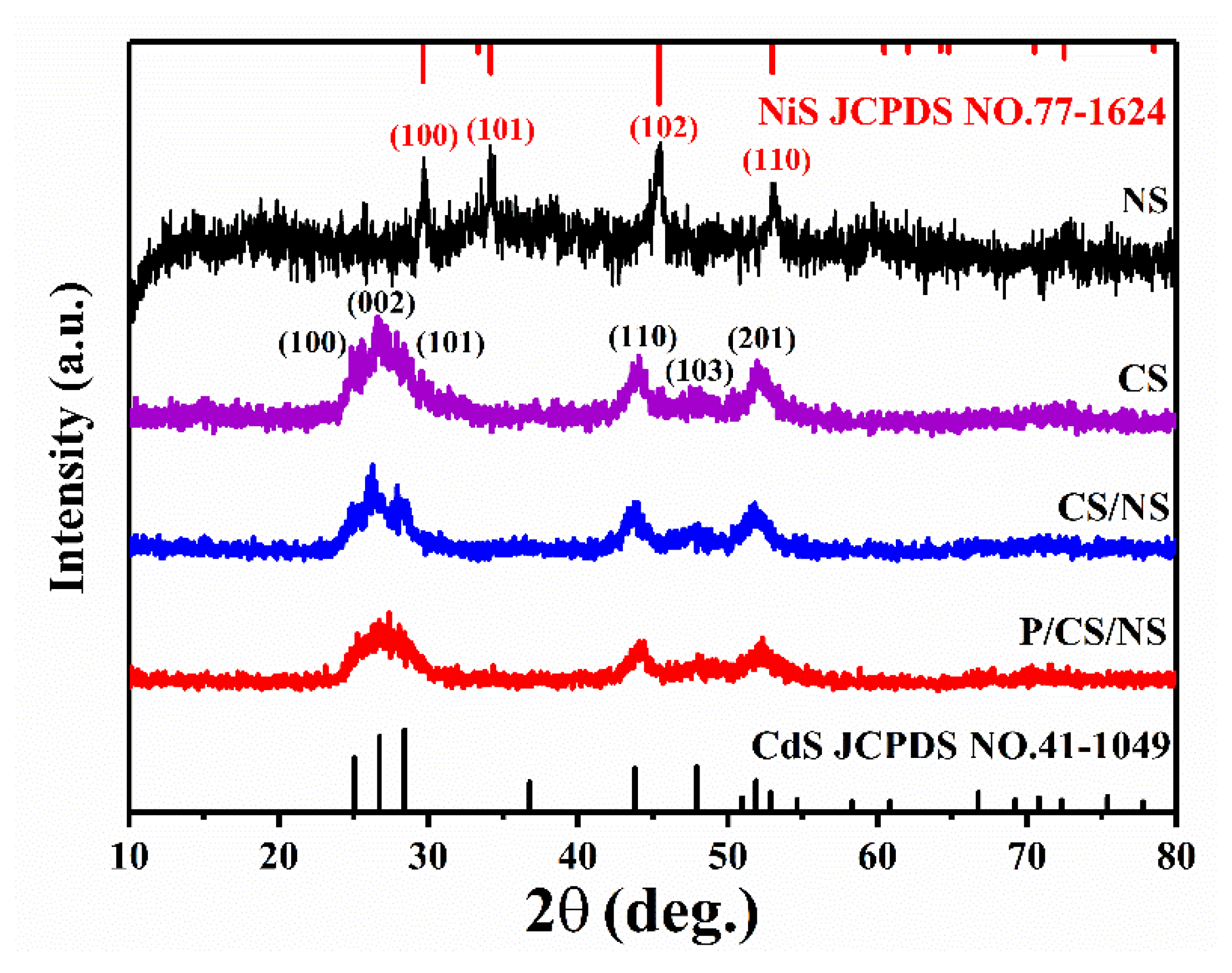
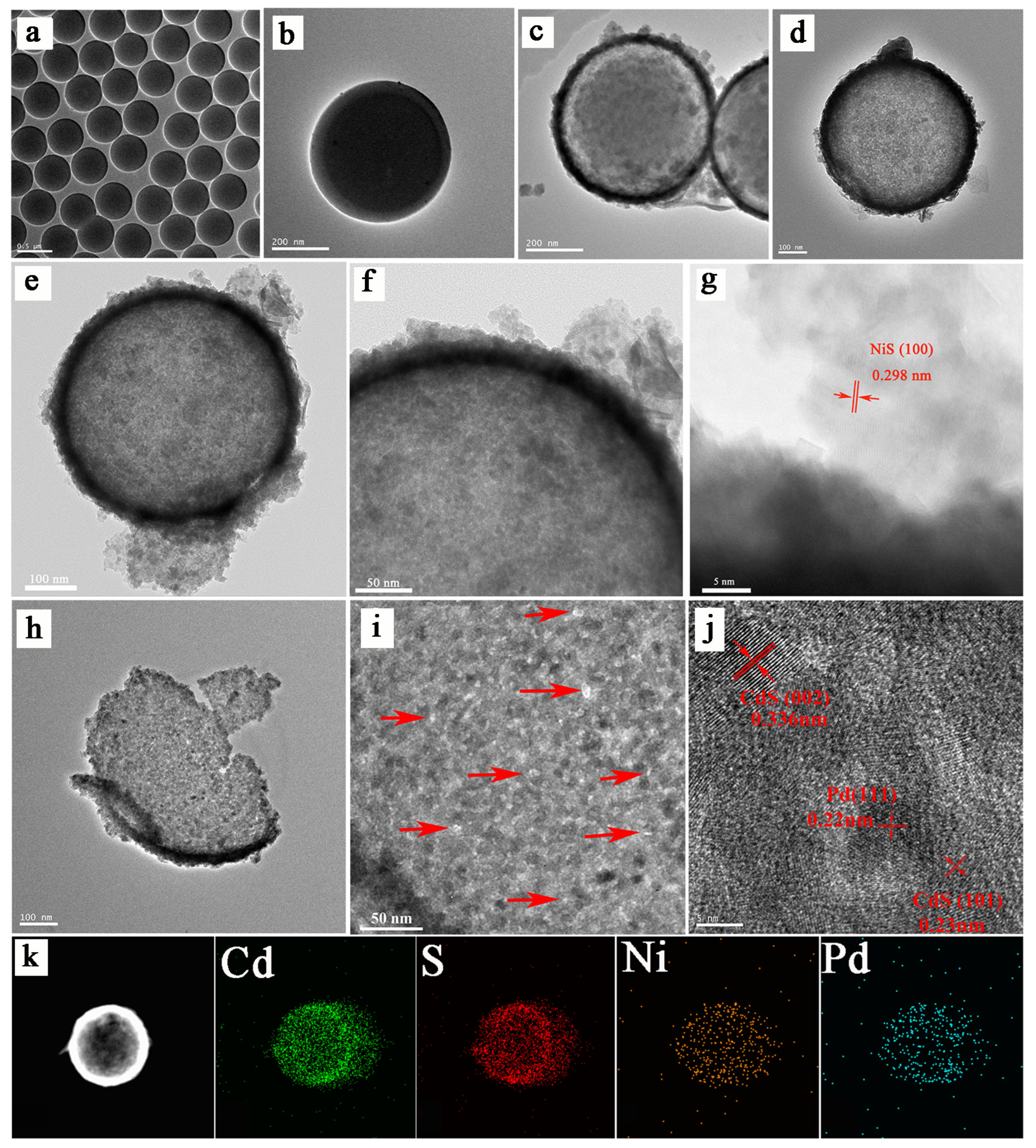
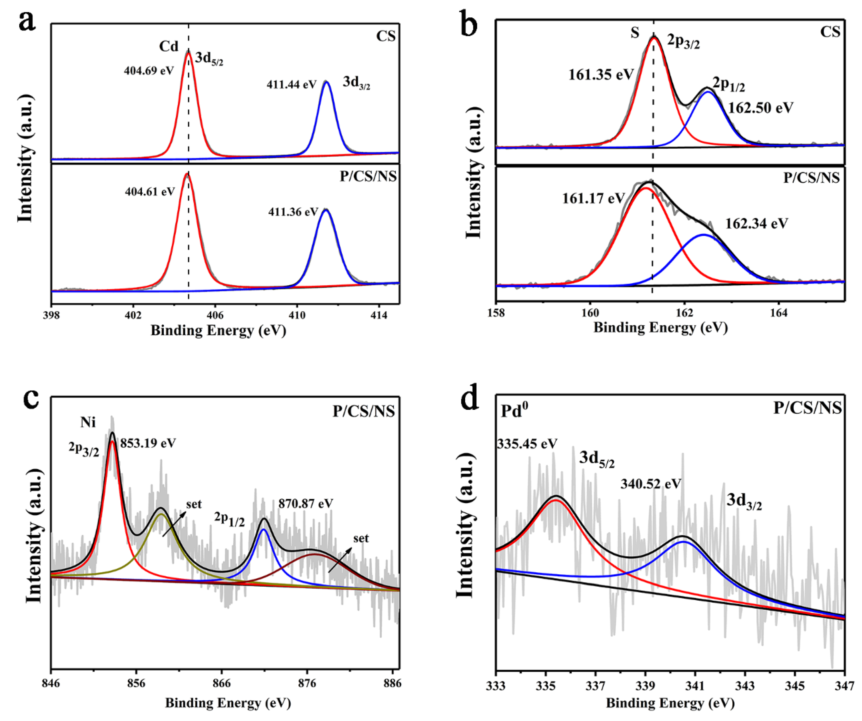
3.1. Characterizations of As-Prepared Photocatalysts
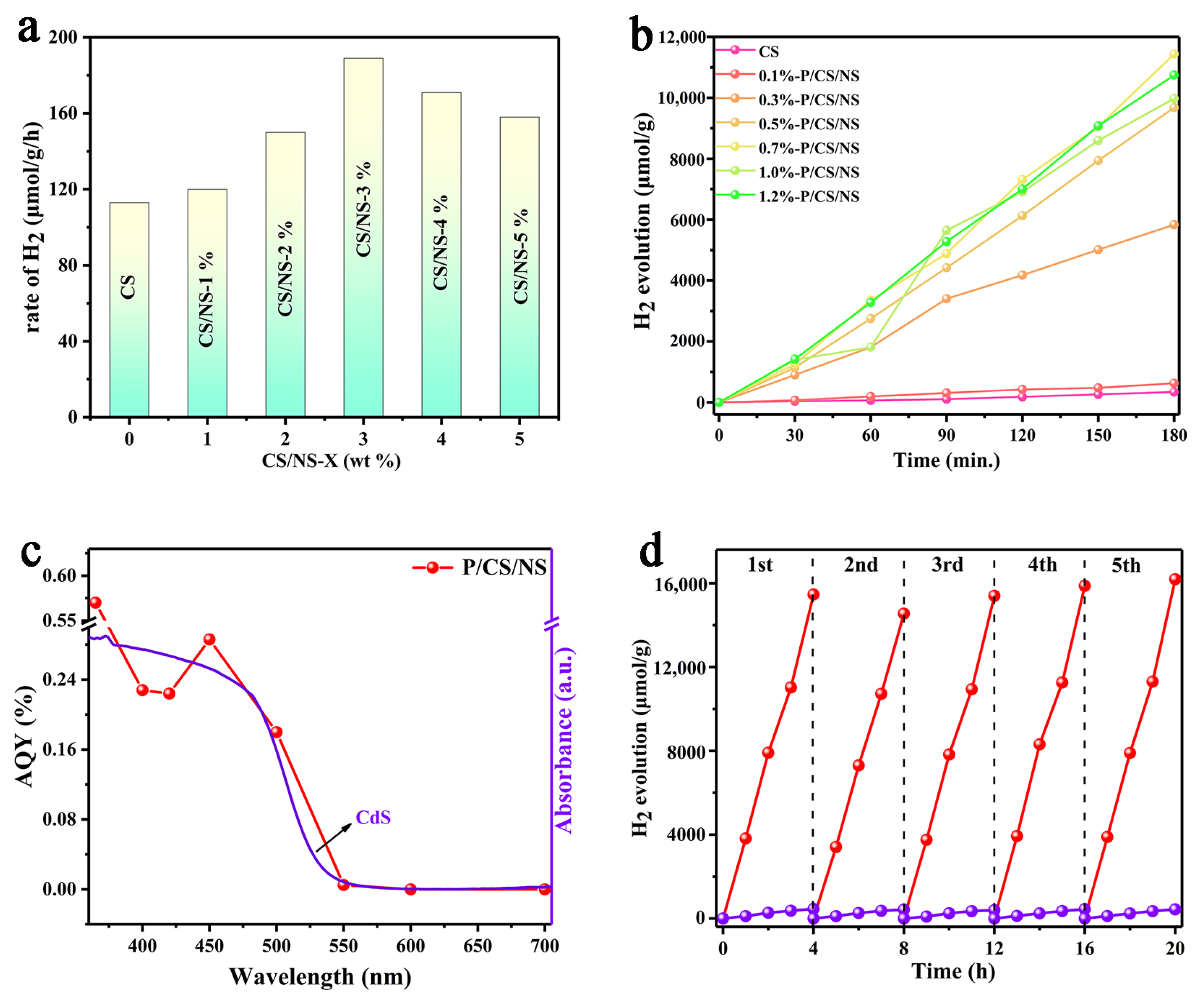
3.2. Photocatalytic H2 Evolution Activity Measurements
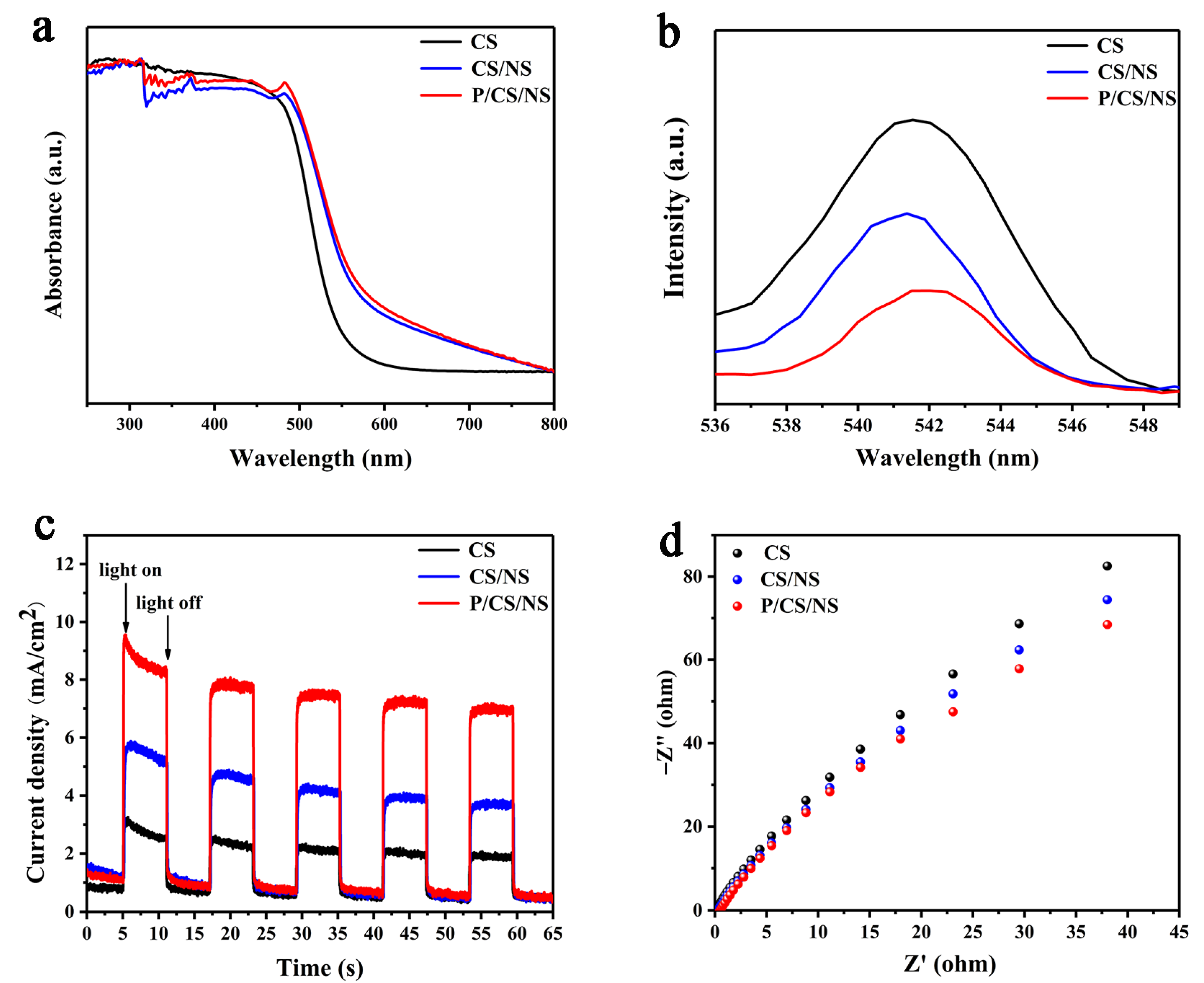
3.3. Photophysical and Electrochemical Properties
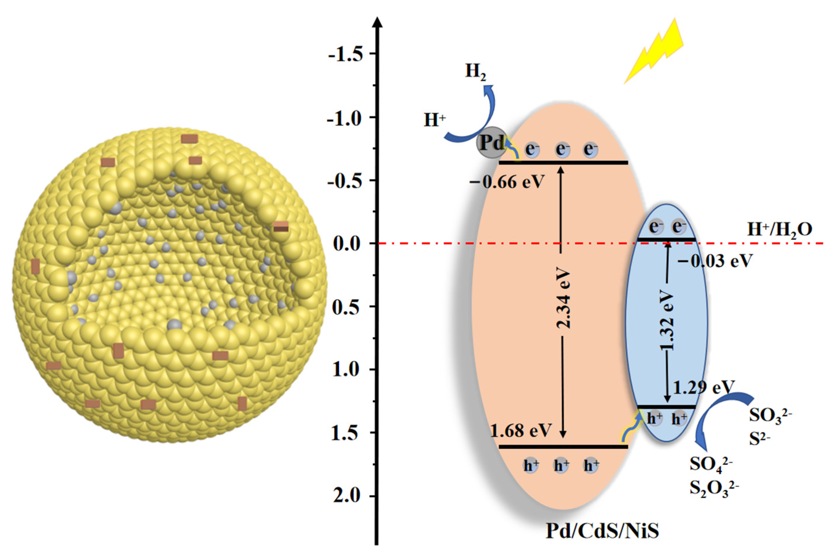
3.4. Photocatalytic Mechanism Analysis
4. Conclusions
Supplementary Materials
Author Contributions
Funding
Data Availability Statement
Conflicts of Interest
References
- Chu, S.; Majumdar, A. Opportunities and challenges for a sustainable energy future. Nature 2012, 488, 294–303. [Google Scholar] [CrossRef] [PubMed]
- Staffell, I.; Scamman, D.; Abad, A.V.; Balcombe, P.; Dodds, P.; Ekins, P.; Shah, N.; Ward, K. The role of hydrogen and fuel cells in the global energy system. Energy Environ. Sci. 2019, 12, 463–491. [Google Scholar] [CrossRef] [Green Version]
- Wang, Z.; Li, C.; Domen, K. Recent developments in heterogeneous photocatalysts for solar-driven overall water splitting. Chem. Soc. Rev. 2019, 48, 2109–2125. [Google Scholar] [CrossRef] [PubMed]
- Gao, C.; Low, J.; Long, R.; Kong, T.; Zhu, J.; Xiong, Y. Heterogeneous Single-Atom Photocatalysts: Fundamentals and Applications. Chem. Rev. 2020, 120, 12175–12216. [Google Scholar] [CrossRef] [PubMed]
- Ye, S.; Shi, W.; Liu, Y.; Li, D.; Yin, H.; Chi, H.; Luo, Y.; Ta, N.; Fan, F.; Wang, X.; et al. Unassisted Photoelectrochemical Cell with Multimediator Modulation for Solar Water Splitting Exceeding 4% Solar-to-Hydrogen Efficiency. J. Am. Chem. Soc. 2021, 143, 12499–12508. [Google Scholar] [CrossRef]
- Xiao, J.; Nishimae, S.; Vequizo, J.; Nakabayashi, M.; Hisatomi, T.; Li, H.; Lin, L.; Shibata, N.; Yamakata, A.; Inoue, Y.; et al. Enhanced Overall Water Splitting by a Zirconium-Doped TaON-Based Photocatalyst. Angew. Chem. Int. Ed. Engl. 2022, 61, e202116573. [Google Scholar] [CrossRef]
- Hisatomi, T.; Domen, K. Reaction systems for solar hydrogen production via water splitting with particulate semiconductor photocatalysts. Nat. Catal. 2019, 2, 387–399. [Google Scholar] [CrossRef]
- Lin, L.; Lin, Z.; Zhang, J.; Cai, X.; Lin, W.; Yu, Z.; Wang, X. Molecular-level insights on the reactive facet of carbon nitride single crystals photocatalysing overall water splitting. Nat. Catal. 2020, 3, 649–655. [Google Scholar] [CrossRef]
- Bai, S.; Jiang, J.; Zhang, Q.; Xiong, Y. Steering charge kinetics in photocatalysis: Intersection of materials syntheses, characterization techniques and theoretical simulations. Chem. Soc. Rev. 2015, 44, 2893–2939. [Google Scholar] [CrossRef]
- Li, X.; Yu, J.; Low, J.; Fang, Y.; Xiao, J.; Chen, X. Engineering heterogeneous semiconductors for solar water splitting. J. Mater. Chem. A 2015, 3, 2485–2534. [Google Scholar] [CrossRef]
- Zhang, J.; Liang, X.; Zhang, C.; Lin, L.; Xing, W.; Yu, Z.; Zhang, G.; Wang, X. Improved Charge Separation in Poly (heptazine-triazine) Imides with Semi-coherent Interfaces for Photocatalytic Hydrogen Evolution. Angew. Chem. Int. Ed. Engl. 2022, 61, e202210849. [Google Scholar] [PubMed]
- Shi, Y.; Li, L.; Xu, Z.; Guo, F.; Shi, W. Construction of full solar-spectrum available S-scheme heterojunction for boosted photothermal-assisted photocatalytic H2 production. Chem. Eng. J. 2023, 459, 141549. [Google Scholar] [CrossRef]
- Sun, J.; Xue, H.; Guo, N.; Song, T.; Hao, Y.; Sun, J.; Zhang, J.; Wang, Q. Synergetic Metal Defect and Surface Chemical Reconstruction into NiCoS4 /ZnS Heterojunction to Achieve Outstanding Oxygen Evolution Performance. Angew. Chem. Int. Ed. Engl. 2021, 60, 19435–19441. [Google Scholar] [CrossRef]
- Wang, W.; Zhang, Y.; Xie, J.; Wang, Y.; Cao, S.; Ping, H.; Zou, Z.; Zeng, H.; Wang, W.; Fu, Z. Bioinspired Strategy for Efficient TiO2/Au/CdS Photocatalysts Based On Mesocrystal Superstructures in Biominerals and Charge-Transfer Pathway in Natural Photosynthesis. ACS. Appl. Mater. Interfaces 2023, 15, 2996–3005. [Google Scholar] [CrossRef] [PubMed]
- Zhao, F.; Zhang, N.; Li, H.; Zhang, X.; Luo, Z.; Wang, Y. Photocatalyst with Chloroplast-like Structure for Enhancing Hydrogen Evolution Reaction. Energy Environ. Mater. 2021, 5, 12239. [Google Scholar] [CrossRef]
- Jin, C.; Rao, S.; Xie, J.; Sun, Z.; Gao, J.; Li, Y.; Li, B.; Liu, S.; Liu, L.; Liu, Q.; et al. Enhanced photocatalytic antibacterial performance by hierarchical TiO2/W18O49Z-scheme heterojunction with Ti3C2Tx-MXene cocatalyst. Chem. Eng. J. 2022, 447, 137469. [Google Scholar] [CrossRef]
- Lei, Y.; Ng, K.; Zhu, Y.; Zhang, Y.; Li, Z.; Xu, S.; Huang, J.; Hu, J.; Chen, Z.; Cai, W.; et al. Mo-activated VC as effective cocatalyst for an enhanced photocatalytic hydrogen evolution activity of CdS. Chem. Eng. J. 2023, 452, 139325. [Google Scholar] [CrossRef]
- Zhou, H.; Wang, M.; Kong, F.; Chen, Z.; Dou, Z.; Wang, F. Facet-Dependent Electron Transfer Regulates Photocatalytic Valorization of Biopolyols. J. Am. Chem. Soc. 2022, 144, 21224–21231. [Google Scholar] [CrossRef]
- Tao, X.; Zhao, Y.; Mu, L.; Wang, S.; Li, R.; Li, C. Bismuth Tantalum Oxyhalogen: A Promising Candidate Photocatalyst for Solar Water Splitting. Adv. Energy Mater. 2018, 8, 1701392. [Google Scholar] [CrossRef]
- Du, S.; Lin, S.; Ren, K.; Li, C.; Zhang, F. Revealing the effects of transition metal doping on CoSe cocatalyst for enhancing photocatalytic H2 production. Appl. Catal. B Environ. 2023, 328, 122503. [Google Scholar] [CrossRef]
- Chong, W.-K.; Ng, B.-J.; Kong, X.; Tan, L.-L.; Putri, L.; Chai, S.-P. Non-metal doping induced dual p-n charge properties in a single ZnIn2S4 crystal structure provoking charge transfer behaviors and boosting photocatalytic hydrogen generation. Appl. Catal. B Environ. 2023, 325, 122372. [Google Scholar] [CrossRef]
- Kumar, S.; Kumar, A.; Rao, V.N.; Kumar, A.; Shankar, M.; Krishnan, V. Defect-Rich MoSUltrathin Nanosheets-Coated Nitrogen-Doped ZnO Nanorod Heterostructures: An Insight into in-Situ-Generated ZnS for Enhanced Photocatalytic Hydrogen Evolution. ACS Appl. Energy Mater. 2019, 2, 5622–5634. [Google Scholar] [CrossRef]
- Xu, Z.; Younis, A.; Xu, H.; Li, S.; Chu, D. Improved super-capacitive performance of carbon foam supported CeOxnanoflowers by selective doping and UV irradiation. RSC Adv. 2014, 4, 35067–35071. [Google Scholar] [CrossRef]
- Xu, Z.; Younis, A.; Chu, D.; Ao, Z.; Xu, H.; Li, S. Electrodeposition of Mesoporous Co3O4Nanosheets on Carbon Foam for High Performance Supercapacitors. J. Nanomater. 2014, 2014, 902730. [Google Scholar] [CrossRef] [Green Version]
- Guo, R.; Hu, X.; Chen, X.; Bi, Z.; Wang, J.; Pan, W. Recent Progress of Three-dimensionally Ordered Macroporous (3DOM) Materials in Photocatalytic Applications: A Review. Small 2023, e2207767. [Google Scholar] [CrossRef]
- Gu, Y.; Wu, A.; Jiao, Y.; Zheng, H.; Wang, X.; Xie, Y.; Wang, L.; Tian, C.; Fu, H. Two-Dimensional Porous Molybdenum Phosphide/Nitride Heterojunction Nanosheets for pH-Universal Hydrogen Evolution Reaction. Angew. Chem. Int. Ed. Engl. 2021, 60, 6673–6681. [Google Scholar] [CrossRef]
- Xiao, M.; Wang, Z.; Lyu, M.; Luo, B.; Wang, S.; Liu, G.; Cheng, H.; Wang, L. Hollow Nanostructures for Photocatalysis: Advantages and Challenges. Adv. Mater. 2019, 31, e1801369. [Google Scholar] [CrossRef]
- Fan, H.; Jin, Y.; Liu, K.; Liu, W. One-Step MOF-Templated Strategy to Fabrication of Ce-Doped ZnInSTetrakaidecahedron Hollow Nanocages as an Efficient Photocatalyst for Hydrogen Evolution. Adv. Sci. 2022, 9, e2104579. [Google Scholar] [CrossRef]
- Navakoteswara, V.; Rao, V.N.; Reddy, N.L.; Preethi, V.; Karthik, M.; Yu, Y.-T.; Yang, J.; Kumari, M.M.; Shankar, M. A critical review on core/shell-based nanostructured photocatalysts for improved hydrogen generation. Int. J. Hydrogen Energy 2023, 48, 11754–11774. [Google Scholar] [CrossRef]
- Cheng, H.; Hou, J.; Takeda, O.; Guo, X.-M.; Zhu, H. A unique Z-scheme 2D/2D nanosheet heterojunction design to harness charge transfer for photocatalysis. J. Mater. Chem. A 2015, 3, 11006–11013. [Google Scholar] [CrossRef]
- Zhang, J.; Yu, Z.; Gao, Z.; Ge, H.; Zhao, S.; Chen, C.; Chen, S.; Tong, X.; Wang, M.; Zheng, Z.; et al. Porous TiONanotubes with Spatially Separated Platinum and CoOx Cocatalysts Produced by Atomic Layer Deposition for Photocatalytic Hydrogen Production. Angew. Chem. Int. Ed. Engl. 2017, 56, 816–820. [Google Scholar] [CrossRef] [PubMed]
- Qiu, B.; Zhu, Q.; Du, M.; Fan, L.; Xing, M.; Zhang, J. Efficient Solar Light Harvesting CdS/CoSHollow Cubes for Z-Scheme Photocatalytic Water Splitting. Angew. Chem. Int. Ed. Engl. 2017, 56, 2684–2688. [Google Scholar] [CrossRef] [PubMed]
- Li, C.; Du, X.; Jiang, S.; Liu, Y.; Niu, Z.; Liu, Z.; Yi, S.; Yue, X. Constructing Direct Z-Scheme Heterostructure by Enwrapping ZnIn2S4 on CdS Hollow Cube for Efficient Photocatalytic H2 Generation. Adv. Sci. 2022, 9, e2201773. [Google Scholar] [CrossRef] [PubMed]
- Sun, Q.; Wang, N.; Yu, J.; Yu, J. A Hollow Porous CdS Photocatalyst. Adv. Mater. 2018, 30, e1804368. [Google Scholar] [CrossRef] [PubMed]
- Lakshmana, N.; Reddy, N.L.; Rao, V.; Kumari, M.; Ravi, P.; Sathish, M.; Shankar, M. Effective shuttling of photoexcitons on CdS/NiO core/shell photocatalysts for enhanced photocatalytic hydrogen production. Mater. Res. Bull. 2018, 101, 223–231. [Google Scholar] [CrossRef]
- Mamiyev, Z.; Balayeva, N. Metal Sulfide Photocatalysts for Hydrogen Generation: A Review of Recent Advances. Catalysts 2022, 12, 1316. [Google Scholar] [CrossRef]
- Wang, B.; Chen, C.; Jiang, Y.; Ni, P.; Zhang, C.; Yang, Y.; Lu, Y.; Liu, P. Rational designing 0D/1D Z-scheme heterojunction on CdS nanorods for efficient visible-light-driven photocatalytic H2 evolution. Chem. Eng. J. 2021, 412, 128690. [Google Scholar] [CrossRef]
- Zheng, N.-C.; Ouyang, T.; Chen, Y.; Wang, Z.; Chen, D.-Y.; Liu, Z.-Q. Ultrathin CdS shell-sensitized hollow S-doped CeO2 spheres for efficient visible-light photocatalysis. Catal. Sci. Technol. 2019, 9, 1357–1364. [Google Scholar] [CrossRef]
- Manchala, S.; Gandamalla, A.; Rao, V.; Venkatakrishnan, S.; Shanker, V. Solar-light responsive efficient H2 evolution using a novel ternary hierarchical SrTiO3/CdS/carbon nanospheres photocatalytic system. J. Nanostructure Chem. 2021, 12, 179–191. [Google Scholar] [CrossRef]
- Ramírez, A.; Hillebrand, P.; Stellmach, D.; May, M.; Bogdanoff, P.; Fiechter, S.; MnOx, E. Mn2O3, and Mn3O4 Electrodeposited Films for the Oxygen Evolution Reaction of Water. J. Phys. Chem. C 2014, 118, 14073–14081. [Google Scholar] [CrossRef]
- Ran, J.; Zhang, J.; Yu, J.; Jaroniec, M.; Qiao, S. Earth-abundant cocatalysts for semiconductor-based photocatalytic water splitting. Chem. Soc. Rev. 2014, 43, 7787–7812. [Google Scholar] [CrossRef] [PubMed]
- Li, K.; Lin, Y.-Z.; Wang, K.; Wang, Y.; Zhang, Y.; Zhang, Y.; Liu, F.-T. Rational design of cocatalyst system for improving the photocatalytic hydrogen evolution activity of graphite carbon nitride. Appl. Catal. B Environ. 2020, 268, 118402. [Google Scholar] [CrossRef]
- Xu, Q.; Zhu, B.; Cheng, B.; Yu, J.; Zhou, M.; Ho, W. Photocatalytic H2 evolution on graphdiyne/g-C3N4 hybrid nanocomposites. Appl. Catal. B Environ. 2019, 255, 117770. [Google Scholar] [CrossRef]
- Xing, M.; Qiu, B.; Du, M.; Zhu, Q.; Wang, L.; Zhang, J. Spatially Separated CdS Shells Exposed with Reduction Surfaces for Enhancing Photocatalytic Hydrogen Evolution. Adv. Funct. Mater. 2017, 27, 1702624. [Google Scholar] [CrossRef]
- Ying, Y.; Lin, Z.; Huang, H. “Edge/Basal Plane Half-Reaction Separation” Mechanism of Two-Dimensional Materials for Photocatalytic Water Splitting. ACS Energy Lett. 2023, 8, 1416–1423. [Google Scholar] [CrossRef]
- Zhao, F.; Law, Y.; Zhang, N.; Wang, X.; Wu, W.; Luo, Z.; Wang, Y. Constructing Spatially Separated Cage-Like Z-scheme Heterojunction Photocatalyst for Enhancing Photocatalytic H2 Evolution. Small 2023, e2208266. [Google Scholar] [CrossRef]
- Bie, C.; Zhu, B.; Wang, L.; Yu, H.; Jiang, C.; Chen, T.; Yu, J. A Bifunctional CdS/MoO2/MoS2 Catalyst Enhances Photocatalytic H2 Evolution and Pyruvic Acid Synthesis. Angew. Chem. Int. Ed. Engl. 2022, 61, e202212045. [Google Scholar] [CrossRef]
- Al-Azri, Z.; Chen, W.-T.; Chan, A.; Jovic, V.; Ina, T.; Idriss, H.; Waterhouse, G. The roles of metal co-catalysts and reaction media in photocatalytic hydrogen production: Performance evaluation of M/TiO2 photocatalysts (M = Pd, Pt, Au) in different alcohol–water mixtures. J. Catal. 2015, 329, 355–367. [Google Scholar] [CrossRef]
- Ismail, A.; Al-Sayari, S.; Bahnemann, D. Photodeposition of precious metals onto mesoporous TiO2 nanocrystals with enhanced their photocatalytic activity for methanol oxidation. Catal. Today 2013, 209, 2–7. [Google Scholar] [CrossRef]
- He, B.; Bie, C.; Fei, X.; Cheng, B.; Yu, J.; Ho, W.; Al-Ghamdi, A.; Wageh, S. Enhancement in the photocatalytic H2 production activity of CdS NRs by Ag2S and NiS dual cocatalysts. Appl. Catal. B Environ. 2021, 288, 119994. [Google Scholar] [CrossRef]
- Meng, X.; Wang, S.; Zhang, C.; Dong, C.; Li, R.; Li, B.; Wang, Q.; Ding, Y. Boosting Hydrogen Evolution Performance of a CdS-Based Photocatalyst: In Situ Transition from Type I to Type II Heterojunction during Photocatalysis. ACS Catal. 2022, 12, 10115–10126. [Google Scholar] [CrossRef]
- Zhang, X.; Liu, T.; Zhao, F.; Zhang, N.; Wang, Y. In-situ-formed Cd and Ag2S decorated CdS photocatalyst with boosted charge carrier spatial separation for enhancing UV-vis-NIR photocatalytic hydrogen evolution. Appl. Catal. B Environ. 2021, 298, 120620. [Google Scholar] [CrossRef]
- Hao, X.; Cui, Z.; Zhou, J.; Wang, Y.; Hu, Y.; Wang, Y.; Zou, Z. Architecture of high efficient zinc vacancy mediated Z-scheme photocatalyst from metal-organic frameworks. Nano Energy 2018, 52, 105–116. [Google Scholar] [CrossRef]
- Xu, H.; Yang, S.; Ma, X.; Huang, J.; Jiang, H. Unveiling charge-separation dynamics in CdS/metal–organic framework composites for enhanced photocatalysis. Acs Catal. 2018, 8, 11615–11621. [Google Scholar] [CrossRef]
- Wang, Y.; Zhao, J.; Hou, W.; Xu, Y. Decoration of CdS nanowires with Ni3S4 nanoballs enhancing H2 and H2O2 production under visible light. Appl. Catal. B Environ. 2022, 310, 121350. [Google Scholar] [CrossRef]
- Xu, J.; Zhong, W.; Gao, D.; Wang, X.; Wang, P.; Yu, H. Phosphorus-enriched platinum diphosphide nanodots as a highly efficient cocatalyst for photocatalytic H2 evolution of CdS. Chem. Eng. J. 2022, 439, 135758. [Google Scholar] [CrossRef]
- Yuan, C.; Lv, H.; Zhang, Y.; Fei, Q.; Xiao, D.; Yin, H.; Lu, Z.; Zhang, Y. Three-dimensional nanoporous heterojunction of CdS/np-rGO for highly efficient photocatalytic hydrogen evolution under visible light. Carbon 2023, 206, 237–245. [Google Scholar] [CrossRef]
- Li, X.; Song, S.; Gao, Y.; Ge, L.; Song, W.; Ma, T.; Liu, J. Identification of the Charge Transfer Channel in Cobalt Encapsulated Hollow Nitrogen-Doped Carbon Matrix@CdS Heterostructure for Photocatalytic Hydrogen Evolution. Small 2021, 17, e2101315. [Google Scholar] [CrossRef]
- Wang, W.; Tao, Y.; Fan, J.; Yan, Z.; Shang, H.; Phillips, D.; Chen, M.; Li, G. Fullerene–Graphene Acceptor Drives Ultrafast Carrier Dynamics for Sustainable CdS Photocatalytic Hydrogen Evolution. Adv. Funct. Mater. 2022, 32, 2201357. [Google Scholar] [CrossRef]

Disclaimer/Publisher’s Note: The statements, opinions and data contained in all publications are solely those of the individual author(s) and contributor(s) and not of MDPI and/or the editor(s). MDPI and/or the editor(s) disclaim responsibility for any injury to people or property resulting from any ideas, methods, instructions or products referred to in the content. |
© 2023 by the authors. Licensee MDPI, Basel, Switzerland. This article is an open access article distributed under the terms and conditions of the Creative Commons Attribution (CC BY) license (https://creativecommons.org/licenses/by/4.0/).
Share and Cite
Wang, X.; Zhao, F.; Zhang, N.; Wu, W.; Wang, Y. Hollow Spherical Pd/CdS/NiS with Carrier Spatial Separation for Photocatalytic Hydrogen Generation. Nanomaterials 2023, 13, 1326. https://doi.org/10.3390/nano13081326
Wang X, Zhao F, Zhang N, Wu W, Wang Y. Hollow Spherical Pd/CdS/NiS with Carrier Spatial Separation for Photocatalytic Hydrogen Generation. Nanomaterials. 2023; 13(8):1326. https://doi.org/10.3390/nano13081326
Chicago/Turabian StyleWang, Xiao, Fei Zhao, Nan Zhang, Wenli Wu, and Yuhua Wang. 2023. "Hollow Spherical Pd/CdS/NiS with Carrier Spatial Separation for Photocatalytic Hydrogen Generation" Nanomaterials 13, no. 8: 1326. https://doi.org/10.3390/nano13081326