Article

A 1.6 kV Ga2O3 Schottky Barrier Diode with a Low Reverse Current of 1.2 × 10⁻⁵ A/cm2 Enabled by Field Plates and N Ion-Implantation Edge Termination

School of Microelectronics, Fudan University, Shanghai 200433, China
*
Author to whom correspondence should be addressed.
Nanomaterials 2024, 14(11), 978; https://doi.org/10.3390/nano14110978
Submission received: 29 April 2024 / Revised: 22 May 2024 / Accepted: 3 June 2024 / Published: 5 June 2024
(This article belongs to the Special Issue Wide-Bandgap and Ultrawide-Bandgap Semiconductor Nanomaterials)

Abstract

:
In this work, by employing field plate (FP) and N ion-implantation edge termination (NIET) structure, the electrical performance of the β-Ga2O3 Schottky barrier diode (SBD) was greatly improved. Ten samples of vertical SBDs were fabricated to investigate the influence of the relative positions of field plates (FPs) and ion implantation on the device performance. The device with the FP of 15 μm and the ion implantation at the edge of the Schottky electrode exhibited a breakdown voltage (Vbr) of 1616 V, a specific on-resistance (Ron,sp) of 5.11 mΩ·cm2, a power figure of merit (PFOM) of 0.511 GW/cm2, and a reverse current density of 1.2 × 10⁻⁵ A/cm2 @ −1000 V. Compared to the control device, although the Ron,sp increased by 1 mΩ·cm2, the Vbr of the device increased by 183% and the PFOM increased by 546.8%. Moreover, the reverse leakage current of the device with the FP and NIET structure decreased by three orders of magnitude. The TCAD simulation revealed that the peak electric field at the interface decreased from 7 MV/cm @ −500 V to 4.18 MV/cm @ −1000 V. These results demonstrate the great potential for the β-Ga2O3 SBD with a FP and NIET structure in power electronic applications.

1. Introduction

β-Ga2O3 has garnered significant attention owing to its ultra-wide bandgap of 4.9 eV and high breakdown electric field of 8 MV/cm, making it a promising candidate for next-generation power electronics [1,2]. The development of the large-scale melt-growth technique for the β-Ga2O3 wafer has enabled cost-effective manufacturing approaches [3]. Moreover, thanks to the outstanding chemical and thermal stability of β-Ga2O3 [4,5], Schottky barrier diodes (SBDs) [6,7,8,9] and metal-oxide-semiconductor field-effect transistors (MOSFETs) [10,11,12,13] fabricated on β-Ga2O3 wafers have demonstrated strong competitiveness. However, there remains a significant disparity in the breakdown electric field between the material’s theoretical prediction and the fabricated β-Ga2O3 SBDs. This discrepancy is primarily owing to the material defects and the electric field concentration at the Schottky electrode edge. Various approaches, such as field plates (FPs) [14,15], the trench structure [16,17,18], thermally oxidized termination [19], and heterogeneous termination [20,21], have been proposed to suppress the electric field concentration. Meanwhile, the ion implantation technique [22,23,24,25], which creates a high-resistance region in β-Ga2O3, is considered highly effective for increasing the breakdown voltage (Vbr) while reducing the reverse leakage current.
Zhou et al. [22] reported a β-Ga2O3 SBD with Mg-implanted edge termination, achieving a Vbr of 1500 V. He and Mg ion implantation were utilized to fabricate β-Ga2O3 SBDs, resulting in a reduced reverse leakage current and enhanced Vbr [26]. Yet, the influence of the ion implantation position and the relative position between the FP and ion implantation on the device performance has not been studied, which could have a significant impact on the electrical characteristics.
Here, β-Ga2O3 SBDs with FP and N ion-implantation edge termination (NIET) have been demonstrated. The device with the FP of 15 μm and the ion implantation at the edge of the Schottky electrode improved the Vbr from 572 V to 1616 V and achieved the power figure of merit (PFOM) of 0.511 GW/cm2. TCAD simulations were employed to analyze the electric field distribution in β-Ga2O3 SBDs, revealing that the FP and NIET structure significantly enhances the device performance.

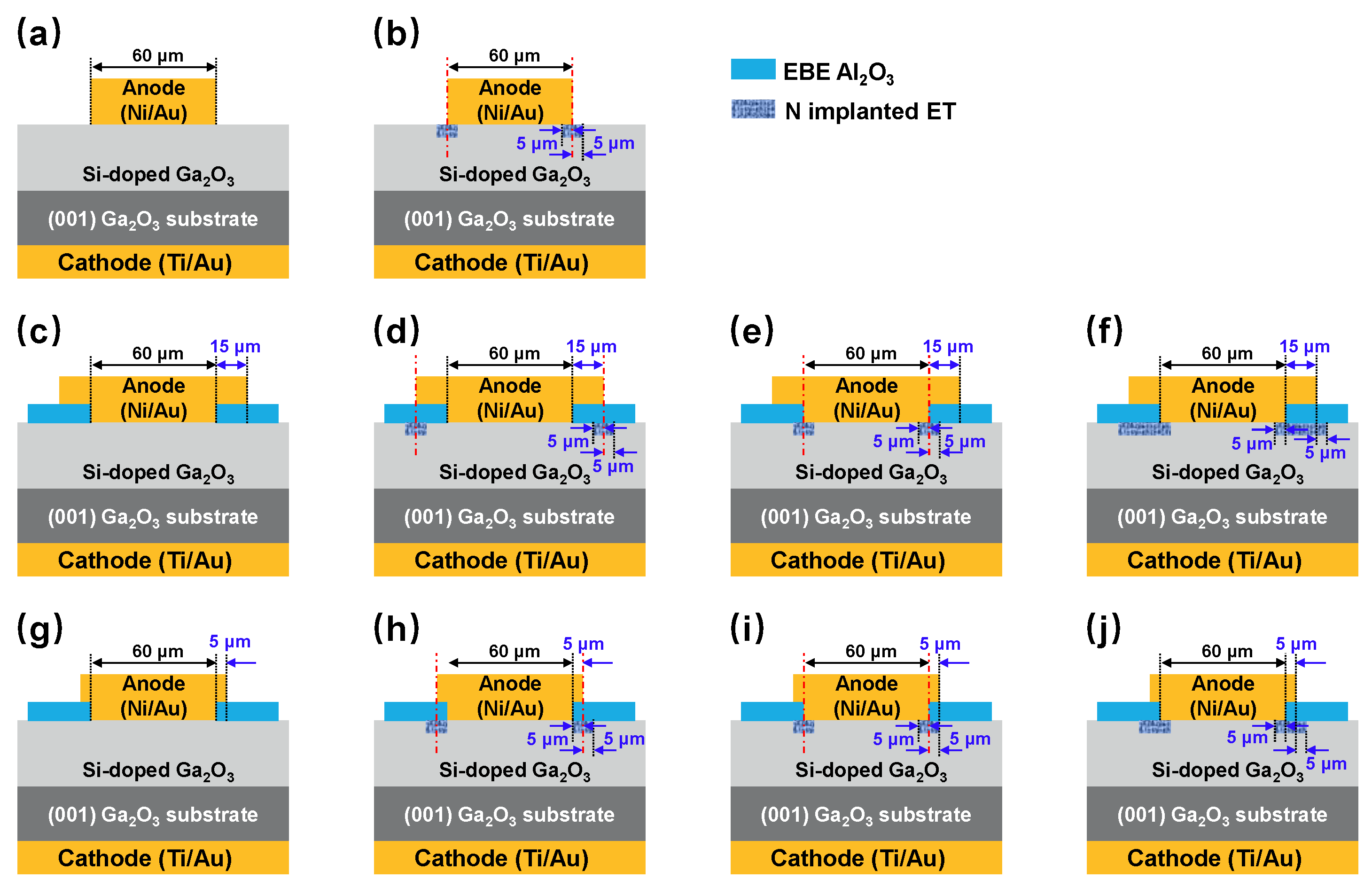
2. Device Structure and Fabrication Process

The β-Ga2O3 SBDs were fabricated on a β-Ga2O3 wafer acquired from Novel Crystal Technology (NCT, Tokyo, Japan). The wafer consists of a 587 μm thick β-Ga2O3 (001) substrate with a Sn doping concentration of ~5.1 × 1018 cm−3 and a 11 μm~3.2 × 1016 cm−3 Si doping epitaxial layer by halide vapor phase epitaxy (HVPE) [27,28]. To investigate the effect of the FP and NIET structure on the device performance, ten samples, shown in Figure 1, were prepared and categorized into three groups based on the FP dimensions. Group 1, Group 2, and Group 3 had FP lengths of 0, 15, and 5 μm, respectively. Sample 1 served as a control without any special treatment.
The device fabrication process is illustrated in Figure 2. Initially, the β-Ga2O3 wafer underwent sequential cleaning with acetone, isopropanol, and deionized (DI) water for 10 min each to eliminate surface contaminants. N ion implantation was performed three times on the wafer to form a 500 nm deep box profile with a simulated doping concentration of around 2~3 × 1019 cm−3. The implantation was carried out at energies/concentrations of 50 keV/5 × 1012 cm−2, 150 keV/1 × 1013 cm−2, and 230 keV/2 × 1013 cm−2 in sequence, as plotted in Figure 3. Then, thermal annealing was executed at 1100 °C for 30 min in N2 to recover the implantation damage and activate the implanted N atoms. The back-Ohmic contact was formed by the electron-beam evaporation (EBE) of Ti/Au (30 nm/100 nm), followed by rapid thermal annealing (RTA) for 60 s at 470 °C in N2. Additionally, 100 nm of Al2O3 was deposited onto the β-Ga2O3 surface via EBE as the FP oxide. The Al2O3 layer was amorphous. During the process, the vacuum was maintained below 5 × 10⁻⁵ Pa, and the growth rate was kept at ~0.1 nm/s. Finally, Schottky anode electrodes were fabricated by evaporating Ni/Au (50 nm/100 nm). The forward current–voltage (IV) and Vbr characteristics were measured using the semiconductor device analyzers Keysight B1500A and B1505A (Santa Rosa, CA, USA), respectively, at room temperature. To evaluate the impact of the NIET on the breakdown performance of the β-Ga2O3 SBD, a physics-based technology computer-aided design (TCAD) simulation in Sentaurus was performed, where the parameters of the β-Ga2O3 in this simulation are shown in Table 1. The Okuto impact ionization model, field-dependent mobility, Shockley Read Hall recombination, and bandgap-narrowing effect were also taken into account.

3. Results and Discussion

3.1. Electrical Properties and Simulations of Devices in Group 1

Figure 4a shows the linear forward current density–voltage (JV) characteristics of Sample 1 and Sample 2. The specific on-resistances (Ron,sp) of Sample 1 and Sample 2 are 4.16 mΩ·cm2 and 4.68 mΩ·cm2, respectively. The increase in the Ron,sp post-ion implantation is attributed to the N-implanted Ga2O3 acting as a current-blocking layer [29,30], thereby reducing the effective area of the Schottky contact. Figure 4b depicts the semi-logarithmic JV curves of Sample 1 and Sample 2, where the turn-on voltage (Von) is extracted at the current density of 1 A/cm2. The Von also increases from 0.84 V to 0.89 V by ion implantation. This could be mainly due to the lateral depletion problem of edge termination [26].
Figure 5a presents the reverse breakdown characteristics, indicating that Sample 2 has a higher Vbr and significantly lower leakage current compared to Sample 1. The leakage current of Sample 2 is less than 1/100th of that of Sample 1 at −500 V. Figure 5b shows the surface electric field distributions of Sample 1 and Sample 2 simulated by the TCAD. The implanted region with a depth of 500 nm is set as the semi-insulating layer because the crystal lattice is damaged by the high-energy N ion implant. The peak electric fields of both samples are located at 30 μm, the edge of the Schottky electrode. Additionally, the vertical electric field distributions along Line Y, which is shown in Figure 2, are plotted in the inset of Figure 5b. The right half of the device is set as the simulation cell, with the center of the device as the origin. The positive x-axis extends to the right, parallel to the material surface, and the positive y-axis extends downward, perpendicular to the material surface. The peak electric field of Sample 1 exceeds 7 MV/cm at −500 V, while, for Sample 2, it is around 6.5 MV/cm. These results show that the ion-implantation ET structure can reduce the peak electric field at the interface and prevent premature device breakdown. Figure 5c,d display the statistical distributions of the reverse breakdown and the leakage current @ −500 V for Sample 1 and Sample 2. The average breakdown voltages of Sample 1 and Sample 2 are 572 V and 920 V, respectively, illustrating a 60.8% increase after ion implantation, which is mainly owing to the electric field concentration suppressed with the ion-implanted ET structure. On the other hand, the average leakage current density @ −500 V of Sample 2 is 5.2 × 10⁻⁷ A/cm2, an approximately nearly three orders of magnitude reduction in the reverse leakage current.

3.2. Electrical Properties and Simulations of Devices in Group 2

Figure 6a depicts the forward JV characteristics of Sample 3 to Sample 6, where the specific on-resistances of Sample 3, Sample 4, Sample 5, and Sample 6 are 4.20 mΩ·cm2, 4.67 mΩ·cm2, 5.11 mΩ·cm2, and 6.31 mΩ·cm2, respectively. Sample 6 shows a 23.4% decrease in the Ron,sp compared to Sample 5, which could be ascribed to the fact that a larger ion-implanted region of Sample 6 leads to more N ion diffusion after annealing. The semi-logarithmic J–V characteristics of Sample 3 to Sample 6 are shown in Figure 6b. The turn-on vlotages of Sample 3, Sample 4, Sample 5, and Sample 6 are 0.84 V, 0.85 V, 0.90 V, and 0.91 V, respectively, where the turn-on voltages of Sample 5 and Sample 6 show a more significant increase. This implies that the ion implantation close to the edge of the Schottky electrode has a greater impact on the Von of the devices.
Figure 7a conveys the reverse breakdown characteristics of Sample 3 to Sample 6. Under the same reverse bias, Sample 3 has a significantly higher leakage current than other samples, confirming that the combined FP and NIET structure results in lower reverse leakage current compared to the conventional FP structure. Figure 7b shows the surface electric field distributions of Sample 3 to Sample 6, with two peak positions at 30 μm and 45 μm, corresponding to the edge of the Schottky electrode and the edge of the FP, respectively. The higher electric field at 30 μm can trigger premature breakdown. The inset displays the vertical electric field along Line Y, revealing that, at 30 μm, the peak electric fields of Sample 5 and Sample 6 are nearly equivalent and significantly lower than those of Sample 3 and Sample 4. This demonstrates that ion implantation at the edge of the Schottky electrode in Sample 5 and Sample 6 effectively suppresses the peak electric field. Meanwhile, the peak electric field of Sample 4 is slightly lower than that of Sample 3, indicating that ion implantation at the edge of the FP has little effect on the peak electric field. Figure 7c,d plot the statistical distributions of Vbr and the reverse leakage current density @ −1000 V for Sample 3 to Sample 6. The average breakdown voltages for Sample 3, Sample 4, Sample 5, and Sample 6 are 1276 V, 1422 V, 1616 V, and 1610 V, respectively, while the average leakage current densities are 2.6 × 10⁻² A/cm2, 4.4 × 10⁻⁴ A/cm2, 1.2 × 10⁻⁵ A/cm2, and 4.1 × 10⁻⁶ A/cm2, respectively. These results suggest that the FP and NIET structure significantly improves the reverse characteristics, with ion implantation at the Schottky electrode edge offering greater enhancement compared to implantation at the FP edge.

3.3. Electrical Properties and Simulations of Devices in Group 3

Figure 8a depicts the linear forward JV characteristics of Sample 7 to Sample 10, with specific on-resistances of 4.05 mΩ·cm2, 4.29 mΩ·cm2, 5.16 mΩ·cm2, and 5.34 mΩ·cm2, respectively. The Ron,sp of Sample 4 increased by 0.47 mΩ·cm² compared to Sample 3, while the Ron,sp of Sample 8 increased by 0.24 mΩ·cm² compared to Sample 7. The smaller increase in Ron,sp for Sample 8 compared to Sample 7 could be mainly caused by the current crowding in the 5 μm FP and NIET composite structure, which results in a lower Ron,sp for the device. Figure 8b presents the semi-logarithmic JV curves of Sample 7 to Sample 10, with turn-on voltages of 0.89 V, 0.90 V, 0.95 V, and 0.95 V, respectively. The Ron,sp and Von of the samples in Group 3 exhibit analogous tendencies to those in Group 2, indicative of a positive correlation between Von and the distance from the ion implantation position to the Schottky contact area, as well as the ion implantation area.
Figure 9a presents the reverse breakdown characteristics of Sample 7 to Sample 10, showing that Sample 7 has a significantly higher leakage current than the other samples, consistent with the results of the Group 2. Figure 9b displays the surface electric field distributions of Sample 7 to Sample 10, with the inset portraying the vertical electric field along Line Y. The electric field at 30 μm remains higher than that at 45 μm. Figure 9c,d depict the Vbr and the reverse leakage current density @ −1000 V statistics for Sample 7 to Sample 10, with average breakdown voltages of 1223 V, 1307 V, 1454 V, and 1469 V, respectively, and average leakage current densities of 4.1 × 10⁻² A/cm2, 3.8 × 10⁻⁵ A/cm2, 6.4 × 10⁻⁶ A/cm2, and 5.5 × 10⁻⁶ A/cm2, respectively. The tendencies of the Vbr and reverse leakage current densities of the samples in Group 3 are consistent with those in Group 2. Additionally, the breakdown voltages of Sample 5 and Sample 6 are higher than those of Sample 9 and Sample 10. This reveals that ion implantation at the edge of the Schottky electrode enhances Vbr more effectively when the FP length is 15 μm.

3.4. Comprehensive Comparisons and Analysis

Table 2 summarizes the Vbr, Ron,sp, Von, and reverse leakage current densities (Jrev) of Samples 1–10. Figure 10a–c show the benchmark plots of Ron,sp versus Vbr, Von versus PFOM, and Jrev versus PFOM, respectively. Sample 5 achieves the highest PFOM, with a very low reverse leakage current of 1.2 × 10⁻⁵ A/cm2 @ −1000 V, although it has a relatively high Von. On the other hand, Sample 4 shows little increase in Von compared to the conventional device; however, its reverse characteristics are inferior to Sample 5. Figure 10d sums up the simulated peak electric fields of Group 2 and Group 3, where the former is generally lower than the latter, suggesting that the devices in Group 2 exhibit superior breakdown tolerance compared to the devices in Group 3. Ion implantation with an FP length of 15 μm significantly improves device electrical performance. Figure 10e,f compare the electrical characteristics of Sample 1 and Sample 5, showing that the β-Ga2O3 SBD with the FP and NIET structure shows a 183% increase in Vbr and a reduction in the reverse leakage current by three orders of magnitude relative to the conventional device. Although the Ron,sp increases by 1 mΩ·cm2, the PFOM of the device increases by 546.8%.

4. Conclusions

In summary, we have examined the effects of the FP and NIET structure on the performance of β-Ga2O3 SBDs. The TCAD simulation suggests that the surface peak electric field of the sample is significantly decreased by the FP and NIET structure. The device with the FP and NIET structure achieves a Vbr of 1616 V, a Ron,sp of 5.11 mΩ·cm2, a PFOM of 0.511 GW/cm2, and a reverse leakage current density of 1.2 × 10⁻⁵ A/cm2 @ −1000 V. These results demonstrate that the FP and NIET structure is highly promising for boosting the performance of β-Ga2O3 power electronics.

Author Contributions

Conceptualization, X.Z. and W.L.; methodology, X.Z. and W.L.; software, X.Z.; validation, X.Z., J.Y., H.Z. and W.L.; formal analysis, X.Z. and J.Y.; investigation, X.Z., H.Z., Y.L. and G.X.; resources, X.Z. and W.L.; data curation, X.Z., J.Y., Y.L., H.Z. and G.X.; writing—original draft preparation, X.Z.; writing—review and editing, X.Z. and W.L.; visualization, X.Z., J.Y., Y.L., H.Z. and G.X.; supervision, J.Y. and H.Z.; project administration, X.Z. and W.L.; funding acquisition, W.L. All authors have read and agreed to the published version of the manuscript.

Funding

This research was funded by Shanghai Municipal Science and Technology Commission under grant 23511102300.

Data Availability Statement

Data are contained within the article.

Acknowledgments

The authors would like to thank Xing Lu and Yuxin Deng, Sun Yat-Sen University, Guangzhou, China, for constructive advice and conducting the ion implantation in this work.

Conflicts of Interest

The authors declare no conflicts of interest.

References

  1. Pearton, S.J.; Yang, J.; Cary, P.H., IV; Ren, F.; Kim, J.; Tadjer, M.J.; Mastro, M.A. A Review of Ga2O3 Materials, Processing, and Devices. Appl. Phys. Rev. 2018, 5, 011301. [Google Scholar] [CrossRef]
  2. Xiao, M.; Wang, B.; Liu, J.; Zhang, R.; Zhang, Z.; Ding, C.; Lu, S.; Sasaki, K.; Lu, G.-Q.; Buttay, C.; et al. Packaged Ga2O3 Schottky Rectifiers with over 60-A Surge Current Capability. IEEE Trans. Power Electron. 2021, 36, 8565–8569. [Google Scholar] [CrossRef]
  3. Kuramata, A.; Koshi, K.; Watanabe, S.; Yamaoka, Y.; Masui, T.; Yamakoshi, S. High-Quality β-Ga2O3 Single Crystals Grown by Edge-Defined Film-Fed Growth. Jpn. J. Appl. Phys. 2016, 55, 1202A2. [Google Scholar] [CrossRef]
  4. Togashi, R.; Nomura, K.; Eguchi, C.; Fukizawa, T.; Goto, K.; Thieu, Q.T.; Murakami, H.; Kumagai, Y.; Kuramata, A.; Yamakoshi, S.; et al. Thermal Stability of β-Ga2O3 in Mixed Flows of H2 and N2. Jpn. J. Appl. Phys. 2015, 54, 041102. [Google Scholar] [CrossRef]
  5. Gucmann, F.; Nadazdy, P.; Husekova, K.; Dobrocka, E.; Priesol, J.; Egyenes, F.; Satka, A.; Rosova, A.; Tapajna, M. Thermal Stability of Rhombohedral α- and Monoclinic β-Ga2O3 Grown on Sapphire by Liquid-Injection MOCVD. Mater. Sci. Semicond. Process. 2023, 156, 107289. [Google Scholar] [CrossRef]
  6. Konishi, K.; Goto, K.; Murakami, H.; Kumagai, Y.; Kuramata, A.; Yamakoshi, S.; Higashiwaki, M. 1-kV Vertical Ga2O3 Field-Plated Schottky Barrier Diodes. Appl. Phys. Lett. 2017, 110, 103506. [Google Scholar] [CrossRef]
  7. Sasaki, K.; Wakimoto, D.; Thieu, Q.T.; Koishikawa, Y.; Kuramata, A.; Higashiwaki, M.; Yamakoshi, S. First Demonstration of Ga2O3 Trench MOS-Type Schottky Barrier Diodes. IEEE Electron Device Lett. 2017, 38, 783–785. [Google Scholar] [CrossRef]
  8. Hu, Z.; Lv, Y.; Zhao, C.; Feng, Q.; Feng, Z.; Dang, K.; Tian, X.; Zhang, Y.; Ning, J.; Zhou, H.; et al. Beveled Fluoride Plasma Treatment for Vertical β-Ga2O3 Schottky Barrier Diode with High Reverse Blocking Voltage and Low Turn-On Voltage. IEEE Electron Device Lett. 2020, 41, 441–444. [Google Scholar] [CrossRef]
  9. Yang, J.; Fares, C.; Elhassani, R.; Xian, M.; Ren, F.; Pearton, S.J.; Tadjer, M.; Kuramata, A. Reverse Breakdown in Large Area, Field-Plated, Vertical β-Ga2O3 Rectifiers. ECS J. Solid State Sci. Technol. 2019, 8, Q3159. [Google Scholar] [CrossRef]
  10. Lv, Y.; Zhou, X.; Long, S.; Song, X.; Wang, Y.; Liang, S.; He, Z.; Han, T.; Tan, X.; Feng, Z.; et al. Source-Field-Plated β-Ga2O3 MOSFET with Record Power Figure of Merit of 50.4 MW/cm2. IEEE Electron Device Lett. 2019, 40, 83–86. [Google Scholar] [CrossRef]
  11. Lv, Y.; Liu, H.; Zhou, X.; Wang, Y.; Song, X.; Cai, Y.; Yan, Q.; Wang, C.; Liang, S.; Zhang, J.; et al. Lateral β-Ga2O3 MOSFETs with High Power Figure of Merit of 277 MW/cm2. IEEE Electron Device Lett. 2020, 41, 537–540. [Google Scholar] [CrossRef]
  12. Montgomery, R.H.; Zhang, Y.; Yuan, C.; Kim, S.; Shi, J.; Itoh, T.; Mauze, A.; Kumar, S.; Speck, J.; Graham, S. Thermal Management Strategies for Gallium Oxide Vertical Trench-Fin MOSFETs. J. Appl. Phys. 2021, 129, 085301. [Google Scholar] [CrossRef]
  13. Zhou, X.; Ma, Y.; Xu, G.; Liu, Q.; Liu, J.; He, Q.; Zhao, X.; Long, S. Enhancement-Mode β-Ga2O3 U-Shaped Gate Trench Vertical MOSFET Realized by Oxygen Annealing. Appl. Phys. Lett. 2022, 121, 223501. [Google Scholar] [CrossRef]
  14. Roy, S.; Bhattacharyya, A.; Peterson, C.; Krishnamoorthy, S. 2.1 kV (001) β-Ga2O3 Vertical Schottky Barrier Diode with High-k Oxide Field Plate. Appl. Phys. Lett. 2023, 122, 152101. [Google Scholar] [CrossRef]
  15. Allen, N.; Xiao, M.; Yan, X.; Sasaki, K.; Tadjer, M.J.; Ma, J.; Zhang, R.; Wang, H.; Zhang, Y. Vertical Ga2O3 Schottky Barrier Diodes with Small-Angle Beveled Field Plates: A Baliga’s Figure-of-Merit of 0.6 GW/cm2. IEEE Electron Device Lett. 2019, 40, 1399–1402. [Google Scholar] [CrossRef]
  16. Li, W.; Hu, Z.; Nomoto, K.; Jinno, R.; Zhang, Z.; Tu, T.Q.; Sasaki, K.; Kuramata, A.; Jena, D.; Xing, H.G. 2.44 kV Ga2O3 Vertical Trench Schottky Barrier Diodes with Very Low Reverse Leakage Current. In Proceedings of the IEEE Annual International Electron Devices Meeting (IEDM), San Francisco, CA, USA, 1–5 December 2018. [Google Scholar]
  17. Li, W.; Nomoto, K.; Hu, Z.; Jena, D.; Xing, H.G. Fin-Channel Orientation Dependence of Forward Conduction in kV-Class Ga2O3 Trench Schottky Barrier Diodes. Appl. Phys. Express 2019, 12, 061007. [Google Scholar] [CrossRef]
  18. Li, W.; Nomoto, K.; Hu, Z.; Jena, D.; Xing, H.G. Field-Plated Ga2O3 Trench Schottky Barrier Diodes With a BV2/Ron,sp of up to 0.95 GW/cm2. IEEE Electron Device Lett. 2020, 41, 107–110. [Google Scholar] [CrossRef]
  19. Wang, Y.; Lv, Y.; Long, S.; Zhou, X.; Song, X.; Liang, S.; Han, T.; Tan, X.; Feng, Z.; Cai, S.; et al. High-Voltage (−201) β-Ga2O3 Vertical Schottky Barrier Diode with Thermally-Oxidized Termination. IEEE Electron Device Lett. 2020, 41, 131–134. [Google Scholar] [CrossRef]
  20. Yan, Q.; Gong, H.; Zhang, J.; Ye, J.; Zhou, H.; Liu, Z.; Xu, S.; Wang, C.; Hu, Z.; Feng, Q.; et al. β-Ga2O3 Hetero-Junction Barrier Schottky Diode with Reverse Leakage Current Modulation and BV2/Ron,sp Value of 0.93 GW/cm2. Appl. Phys. Lett. 2021, 118, 122102. [Google Scholar] [CrossRef]
  21. Gong, H.H.; Yu, X.X.; Xu, Y.; Chen, X.H.; Kuang, Y.; Lv, Y.J.; Yang, Y.; Ren, F.-F.; Feng, Z.H.; Gu, S.L.; et al. β-Ga2O3 Vertical Heterojunction Barrier Schottky Diodes Terminated with p-NiO Field Limiting Rings. Appl. Phys. Lett. 2021, 118, 202102. [Google Scholar] [CrossRef]
  22. Zhou, H.; Yan, Q.; Zhang, J.; Lv, Y.; Liu, Z.; Zhang, Y.; Dang, K.; Dong, P.; Feng, Z.; Feng, Q.; et al. High-Performance Vertical β-Ga2O3 Schottky Barrier Diode with Implanted Edge Termination. IEEE Electron Device Lett. 2019, 40, 1788–1791. [Google Scholar] [CrossRef]
  23. Yang, J.; Ren, F.; Tadjer, M.; Pearton, S.J.; Kuramata, A. 2300V Reverse Breakdown Voltage Ga2O3 Schottky Rectifiers. ECS J. Solid State Sci. Technol. 2018, 7, Q92. [Google Scholar] [CrossRef]
  24. Lin, C.-H.; Yuda, Y.; Wong, M.H.; Sato, M.; Takekawa, N.; Konishi, K.; Watahiki, T.; Yamamuka, M.; Murakami, H.; Kumagai, Y.; et al. Vertical Ga2O3 Schottky Barrier Diodes with Guard Ring Formed by Nitrogen-Ion Implantation. IEEE Electron Device Lett. 2019, 40, 1487–1490. [Google Scholar] [CrossRef]
  25. Gao, Y.; Li, A.; Feng, Q.; Hu, Z.; Feng, Z.; Zhang, K.; Lu, X.; Zhang, C.; Zhou, H.; Mu, W.; et al. High-Voltage β-Ga2O3 Schottky Diode with Argon-Implanted Edge Termination. Nanoscale Res. Lett. 2019, 14, 8. [Google Scholar] [CrossRef] [PubMed]
  26. Zhang, Y.; Zhang, J.; Feng, Z.; Hu, Z.; Chen, J.; Dang, K.; Yan, Q.; Dong, P.; Zhou, H.; Hao, Y. Impact of Implanted Edge Termination on Vertical β-Ga2O3 Schottky Barrier Diodes under OFF-State Stressing. IEEE Trans. Electron Devices 2020, 67, 3948–3953. [Google Scholar] [CrossRef]
  27. Murakami, H.; Nomura, K.; Goto, K.; Sasaki, K.; Kawara, K.; Thieu, Q.T.; Togashi, R.; Kumagai, Y.; Higashiwaki, M.; Kuramata, A.; et al. Homoepitaxial Growth of β-Ga2O3 Layers by Halide Vapor Phase Epitaxy. Appl. Phys. Express 2014, 8, 015503. [Google Scholar] [CrossRef]
  28. Goto, K.; Konishi, K.; Murakami, H.; Kumagai, Y.; Monemar, B.; Higashiwaki, M.; Kuramata, A.; Yamakoshi, S. Halide Vapor Phase Epitaxy of Si Doped β-Ga2O3 and Its Electrical Properties. Thin Solid Films 2018, 666, 182–184. [Google Scholar] [CrossRef]
  29. Wong, M.H.; Goto, K.; Murakami, H.; Kumagai, Y.; Higashiwaki, M. Current Aperture Vertical β-Ga2O3 MOSFETs Fabricated by N- and Si-Ion Implantation Doping. IEEE Electron Device Lett. 2019, 40, 431–434. [Google Scholar] [CrossRef]
  30. Wong, M.H.; Lin, C.-H.; Kuramata, A.; Yamakoshi, S.; Murakami, H.; Kumagai, Y.; Higashiwaki, M. Acceptor Doping of β-Ga2O3 by Mg and N Ion Implantations. Appl. Phys. Lett. 2018, 113, 102103. [Google Scholar] [CrossRef]
Figure 1. Cross-sectional schematics of (a) Sample 1, (b) Sample 2, (c) Sample 3, (d) Sample 4, (e) Sample 5, (f) Sample 6, (g) Sample 7, (h) Sample 8, (i) Sample 9, and (j) Sample 10.
Nanomaterials 14 00978 g001
Figure 2. Process flow of the fabricated β-Ga2O3 SBDs with the FP and NIET structure.
Nanomaterials 14 00978 g002
Figure 3. N-implanted total concentration after three N ion implantations.
Nanomaterials 14 00978 g003
Figure 4. (a) Forward J–V characteristics and Ron,sp; (b) semi-log scale J–V characteristics and Von of Sample 1 and Sample 2.
Nanomaterials 14 00978 g004
Figure 5. (a) Reverse characteristics; (b) simulations of the surface electric field distributions; (c) statistical plots of Vbr; (d) statistical plots of the reverse leakage current densities of Sample 1 and Sample 2.
Nanomaterials 14 00978 g005
Figure 6. (a) Forward J–V characteristics and Ron,sp; (b) semi-log scale JV characteristics and Von of Sample 3 to Sample 6.
Nanomaterials 14 00978 g006
Figure 7. (a) Reverse characteristics; (b) simulations of the surface electric field distributions; (c) statistical plots of Vbr; (d) statistical plots of reverse leakage current densities of Sample 3 to Sample 6.
Nanomaterials 14 00978 g007
Figure 8. (a) Forward JV characteristics and Ron,sp; (b) semi-log scale JV characteristics and Von of Sample 7 to Sample 10.
Nanomaterials 14 00978 g008
Figure 9. (a) Reverse characteristics; (b) simulations of the surface electric field distributions; (c) statistical plots of Vbr; (d) statistical plots of reverse leakage current densities of Sample 7 to Sample 10.
Nanomaterials 14 00978 g009
Figure 10. Benchmark plots of (a) Ron,sp vs. Vbr, (b) Von vs. PFOM, (c) and reverse leakage current densities @ −1000 V vs. PFOM. (d) The peak electric fields of Group 2 and Group 3. (e) Forward J–V characteristics. (f) Reverse characteristics of Sample 1 and Sample 5.
Nanomaterials 14 00978 g010
Table 1. Material parameters used in this simulation.
Parametersβ-Ga2O3
Bandgap (eV)4.8
Affinity (eV)4.0
NC (cm−3)3.7 × 10¹⁸
NV (cm−3)5.0 × 10¹⁸
Relative permittivity10.0
Electron mobility (cm2 V−1 s−1)200
Saturation velocity (cm s−1)2 × 10⁷
Table 2. Vbr, Ron,sp, Von, and reverse leakage current densities of Samples 1–10.
DeviceVbr (V)Ron,sp (mΩ·cm2)Von (V)Jrev (A/cm2 @ −1000 V)
Sample 15724.160.84
Sample 29204.680.89
Sample 312764.200.842.6 × 10−2
Sample 414224.670.854.4 × 10−4
Sample 516165.110.901.2 × 10−5
Sample 616106.310.914.1 × 10−6
Sample 712234.050.894.1 × 10−2
Sample 813074.290.903.8 × 10−5
Sample 914545.160.956.4 × 10−6
Sample 1014695.340.955.5 × 10−6
Disclaimer/Publisher’s Note: The statements, opinions and data contained in all publications are solely those of the individual author(s) and contributor(s) and not of MDPI and/or the editor(s). MDPI and/or the editor(s) disclaim responsibility for any injury to people or property resulting from any ideas, methods, instructions or products referred to in the content.

