Article

Distinguishing the Charge Trapping Centers in CaF2-Based 2D Material MOSFETs

1
School of Physical Science and Technology, Inner Mongolia University, Hohhot 010021, China
2
State Key Laboratory of Superlattices and Microstructures, Institute of Semiconductors, Chinese Academy of Sciences, Beijing 100083, China
3
Ordos Institute of Technology, Ordos 017000, China
*
Authors to whom correspondence should be addressed.
Nanomaterials 2024, 14(12), 1038; https://doi.org/10.3390/nano14121038
Submission received: 24 April 2024 / Revised: 1 June 2024 / Accepted: 11 June 2024 / Published: 16 June 2024

Abstract

:
Crystalline calcium fluoride (CaF2) is drawing significant attention due to its great potential of being the gate dielectric of two-dimensional (2D) material MOSFETs. It is deemed to be superior to boron nitride and traditional silicon dioxide (SiO2) because of its larger dielectric constant, wider band gap, and lower defect density. Nevertheless, the CaF2-based MOSFETs fabricated in the experiment still present notable reliability issues, and the underlying reason remains unclear. Here, we studied the various intrinsic defects and adsorbates in CaF2/molybdenum disulfide (MoS2) and CaF2/molybdenum disilicon tetranitride (MoSi2N4) interface systems to reveal the most active charge-trapping centers in CaF2-based 2D material MOSFETs. An elaborate Table comparing the importance of different defects in both n-type and p-type devices is provided. Most impressively, the oxygen molecules (O2) adsorbed at the interface or surface, which are inevitable in experiments, are as active as the intrinsic defects in channel materials, and they can even change the MoSi2N4 to p-type spontaneously. These results mean that it is necessary to develop a high-vacuum packaging process, as well as prepare high-quality 2D materials for better device performance.

1. Introduction

Two-dimensional (2D) materials offer new possibilities for advancing Moore’s Law due to their ultra-thin thickness and smooth surface with no dangling bonds [1,2,3,4,5,6,7,8,9]. The ultra-scaled channel places higher demands on the quality and reliability of gate dielectric materials. However, common oxides (such as SiO2 [10], hafnium dioxide (HfO2) [11], and aluminum trioxide (Al2O3) [12]) that are used in silicon technologies are non-layered, which makes it difficult for them to form a good interface with 2D channels. To deal with the problem, 2D dielectrics such as hexagonal boron nitride (h-BN) have been studied [13]. However, the band gap (~6 eV) and dielectric constant (5.06 ε) of h-BN are not satisfying for dielectric materials [14]. Its band offset with 2D materials is not large enough, which will lead to many reliability problems [15].
Recent experimental preparation of crystalline CaF2 provides a promising solution to the dilemma [16,17]. By using molecular beam epitaxy (MBE), crystalline CaF2 can be grown on a silicon or germanium substrate [18]. It has a larger bandgap (12.1 eV) and dielectric constant (8.43 ε) than h-BN [19]. The grown CaF2 is terminated by F atoms, which means that there are no dangling bond on its surface [20]. At the same time, wafer-scale CaF2 was prepared by the magnetron sputtering method as a substrate for optoelectronic devices, resulting in the formation of good van der Waals devices with Tin disulfide (SnS2) and Tungsten disulfide (WS2). The electronic mobility and photoresponsivity of the devices were improved by an order of magnitude higher compared to SiO2-based devices [21]. Another important point is that CaF2 itself is stable in air, and is not easily dissolved in water [22]. CaF2 can form good I-band alignment with many 2D materials, such as silicon carbide (SiC). The valence band offset of 2D SiC/CaF2 is as high as 3.5 eV, and even if there are carbon antisite and interstitial defects on the 2D SiC surface, it will not affect CaF2 [23]. This means that it will be very advantageous as a gate dielectric for semiconductor devices.
Nevertheless, notable device reliability issues were still observed in CaF2-based MOSFETs [19,22,24,25], which contradicts the perfect electrical properties of CaF2. For example, the ID-VG hysteresis is significant (although, lower than that in MoS2/SiO2 FET), and it shows obvious variability when the same device is operated at different scanning times. On the other hand, when different devices are operated under the same VD, the ID-VG characteristics such as on/off current ratio and subthreshold swing (SS) (150–90 mV dec−1) differ greatly [19]. In addition, some devices with large negative threshold voltage (Vth) are prone to fail due to the bias overload of the CaF2 layer. The physical origin of hysteresis and threshold voltage shift is widely attributed to the charge trapping and de-trapping of microscopic defects [26,27,28,29,30,31,32], and the strength of the charge trapping effect is closely related to the type of defects [33,34,35,36]. In graphene/CaF2 FETs, the hysteresis and bias–temperature instabilities (BTI) phenomenon are both observed due to the presence of defects. They are not detrimental to device performance due to the intrinsic advantage of CaF2, but the problem cannot be avoided [37]. The hysteresis is also observed in ReS2 FETs, and it is subjected to variations in temperature, sweeping gate voltage, and pressure during experiments, demonstrating the existence of a charge-trapping and de-trapping effect [38].
The presence of trapping centers at the interface not only affects the reliability of transistors, but also has an impact on other kinds of semiconductor devices, such as thermoelectric devices composed of tin dioxide (SnO2) [39] and solar cell devices composed of perovskite materials such as perovskite solar cells (PSCs) [40]. Therefore, distinguishing active trapping centers, and then finding ways to eliminate them, is crucial for the improvement of semiconductor devices. Unfortunately, it is difficult to determine the specific contribution of each kind of defect to the charge-trapping process through experiments. Under such circumstances, we decides to use principles calculations to distinguish the active charge-trapping centers in CaF2-based 2D MOSFETs first, and then provide guidance to experimental researchers to analyze and improve the performance and reliability of their devices.
In this work, realistic MoS2/CaF2 and MoSi2N4/CaF2 interface models have been constructed to study the charge-trapping centers in various positions. CaF2 is designed as a 5-layer structure, which is consistent with the experimental report [19,41]. The fabricated device in the experiment contains a 2-layer MoS2 and a 2 nm thick CaF2, which is 5 layers. At the same time, 13 types of defects were systematically investigated, and several positions for each type of defect were studied to avoid randomness. When analyzing defects, we not only considered the defect energy levels, but also the defect formation energy and their importance in n-type and p-type transistors, respectively. To ensure the accuracy of the data, Heyd–Scuseria–Ernzerhof (HSE) hybrid functionals were used, even though they require a large amount of computing resources.

2. Materials and Methods
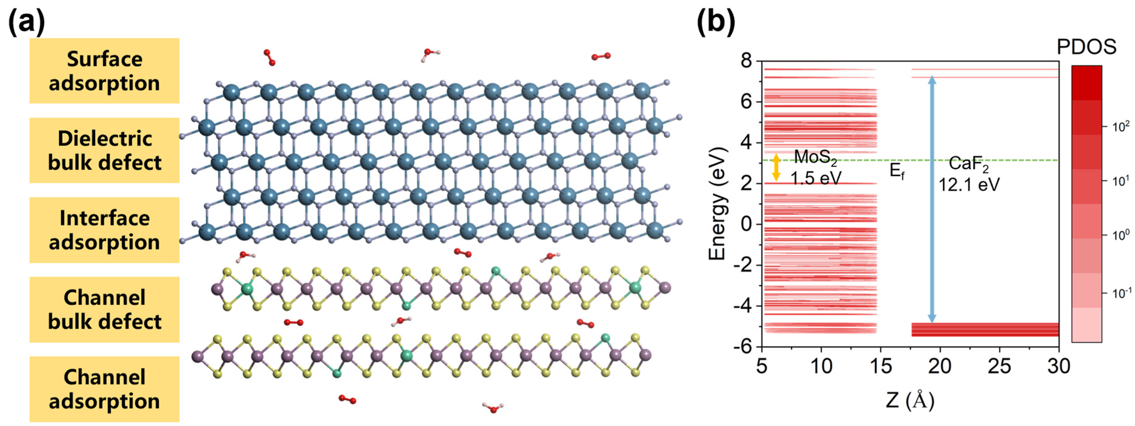
Among the 2D materials, MoS2 is one of the most widely used semiconductors [42,43,44,45]. It has a direct band gap of 1.8 eV, and has been used to design high-performance electronic and optoelectronic devices [5]. On the other hand, there are also some new materials being synthetized, such as the MoSi2N4 [46]. MoSi2N4 is very promising because of the excellent photocatalytic performance [47], mechanical strength [48], and electrical transportability [49]. Therefore, we construct both MoS2/CaF2 and MoSi2N4/CaF2 interface models to make the simulation results representative. The lattice parameter of CaF2, MoS2, and MoSi2N4 is 3.90 Å, 3.16 Å, and 2.91 Å, respectively. To achieve good lattice matching, the primary cell of MoS2 is repeated five times to contact the CaF2 cell, which is repeated four times. The final CaF2 deformation is only 1.28%. Similarly, the primary cell of MoSi2N4 is repeated four times to contact the CaF2, while the CaF2 deformation is repeated three times and is only 0.52%.
To make the results reliable, different types of defects/impurities, not only within the material, but also at the interfaces and surfaces, were studied. For CaF2, even though previous studies have shown that it only contains a very small number of F defects (VF), for the sake of data reliability, research was still conducted on VF defects. Meanwhile, our research found that VF contributes two electrons to CBM, which had not been discovered by previous researchers. For MoS2, we considered S vacancy defect (VS), Mo vacancy defects (VMo), MoS3 vacancy defect (VMoS3) and MoS6 vacancy defect (VMoS6) at different spatial locations. MoS2 is composed of one Mo atom in the middle and three S atoms on the upper and lower surfaces. A MoS3 defect is defined as the loss of a Mo atom and three S atoms connected to it, either in the upper or lower layers. The MoS6 defect is formed by the loss of both the Mo atom in the middle and the six S atoms connected to it. On the other hand, considering that gas adsorption is occurs very easily in the process of device manufacturing, we also studied the water and oxygen molecules that adsorbed at different positions. For a more intuitive display of defects and adsorption, the related structural diagrams are shown in following figures. For MoSi2N4, both its N vacancies (VN) and Si vacancies (VN) were studied simultaneously. Same as MoS2, gas adsorption in MoSi2N4 during preparation is also a factor that may affect device stability. The adsorption of O2 and water molecules (H2O) was studied in CaF2-MoSi2N4.
All the first-principles calculations were performed by the software PWmat [50,51]. The SG15 pseudopotential [52] was adopted, and the plane wave cutoff energy was 50 Ry. The Perdew–Burke–Ernzerhof (PBE) functional was used for structural relaxation with a convergence criterion of 10−5 eV/Å. The HSE [53] functional was used in the calculation of electronic structures to improve the accuracy of calculations. All calculations were performed using gamma points (0,0,0) considering the largeness of the supercells, and this is a common strategy to deal with large models [34,35]. VdW-D3 was used to correct the interlayer interaction of the material. The DFT-D3 energy formula is as follows: E D F T D 3 = E K S D F T E d i s p , E K S D F T is the usual self-consistent KS energy and E d i s p is the dispersion correction as a sum of two- and three-body energies [54]. The equilibrium distance between the MoS2 and CaF2 and between the CaF2 and MoSi2N4 was 2.89 Å and 2.93 Å, respectively. For MoS2, the impact of point defects on the equilibrium distance was not significant, only 1.04%. For larger defects, there may have been some impacts, among which VMoS3 decreased the distance by 8.65% to 2.64 Å. O2 adsorption resulted in an equilibrium distance of 3.03 Å, which represented an increase of 5.21%. For MoSi2N4, the VN defect showed a change in the equilibrium distance between CaF2-MoSi2N4, with an equilibrium position of 2.72 Å, representing a 7.17% decrease. H2O adsorption resulted in an equilibrium position of 3.10 Å, which represented an increase of 5.80%. The data above show that defects and adsorption can slightly change the equilibrium distance between interfaces, but their impact is not significant. All the calculation processes are shown in Figure 1.

3. Results

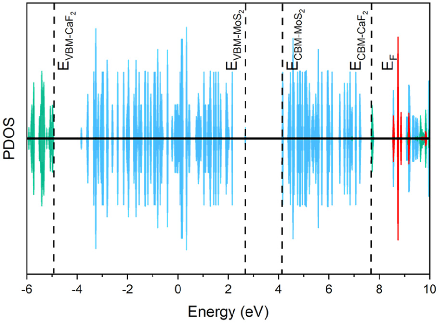
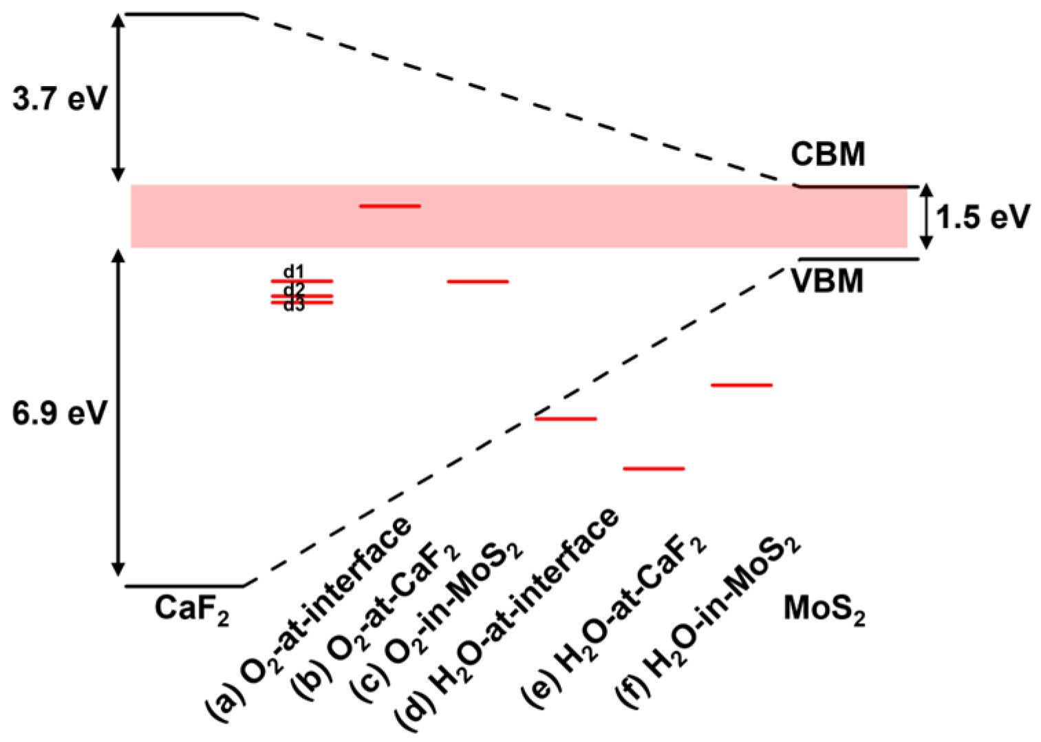
3.1. The Charge-Trapping Centers in CaF2-MoS2

The CaF2-MoS2 interface models are shown in Figure 2a. Blue, gray, purple, yellow, white, and red spheres are used in the figure to represent Ca, F, Mo, S, H, and O atoms. Figure 2a shows the adsorption and defects (green spheres) present at different interfaces and surfaces of CaF2-MoS2. A 5-layer CaF2 is adopted because the experimental MBE grown CaF2 is about 2 nm thick. The band alignments that manifested by the projected density of states (PDOS) are shown in Figure 2b. The red part in the figure represents the data of DOS, and the depth of the color represents the size of PDOS values. It can be seen that the VBM (valence band maximum) and CBM (conduction band minimum) are provided by MoS2, and the band offsets are greater than 2 eV, which makes charge tunneling difficult. All Fermi energy levels have been reset to zero, indicated by a green dotted line in the graph. The defect energy level and band offset have a direct impact on the charge-trapping activity. Although the vacuum levels were not adjusted, this does not affect the conclusions reached. This confirms that using CaF2 as the gate of 2D material MOSFETs is likely to obtain good device reliability [41]. Therefore, when considering practical applications, we believe that the reliability issues should stem from some intrinsic or external charge-trapping centers.

3.1.1. The Charge-Trapping Centers in CaF2

Intuitively, we should first study the F vacancy defect in the CaF2 layer. However, it has been demonstrated in experiments that generating defects in CaF2 is not easy [19]. Furthermore, it has been proven by a first-principle calculation that even though F vacancies (VF) and Ca vacancies (VGa) exist, there is no defect state near the band edge of channel material due to the large band offset between the two materials [55]. Nevertheless, to make the conclusion more rigorous, we still conducted relevant calculations on the VF. In Figure 3, the energy levels of CaF2, MoS2, and VF are represented by green, blue, and red, respectively. In the calculation, both vdW and electron spin are considered, and the randomness of VF positions is also taken into account. For ease of observation, the PDOS value of VF in Figure 3 has been expanded 50 times. As the focus is on the defect energy level of VF, it does not affect the results. The band alignment of CaF2 and MoS2 here is consistent with Figure 2b, and MoS2 provides VBM and CBM. The offset between the VF defect energy level and CBM is 4.43 eV, indicating that even with defects, it is not easy to trap charges. Consequently, we turn our attention to the trapping centers inside the channel material, in the semiconductor/dielectric interface, and at the dielectric surface.

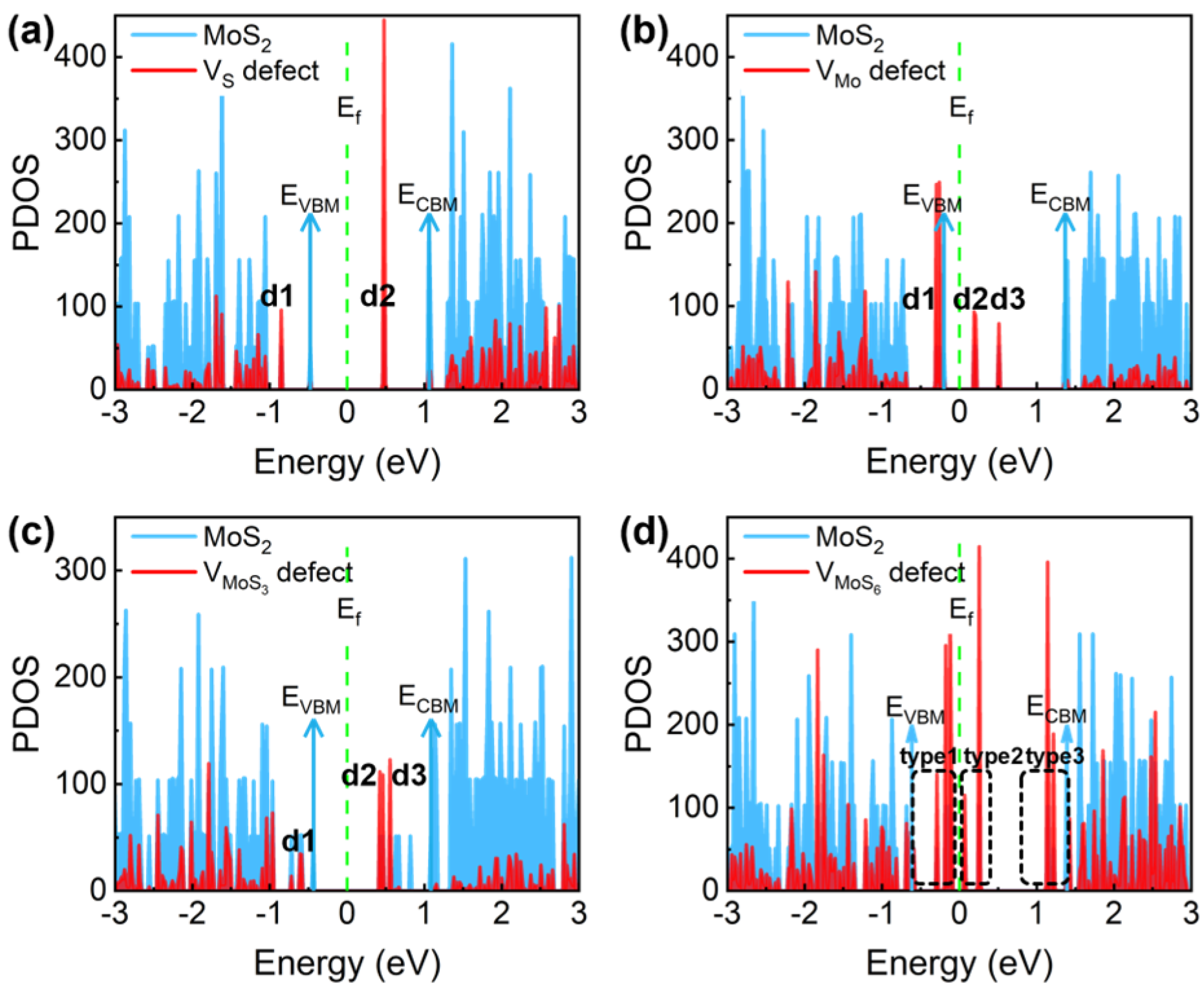
3.1.2. The Charge-Trapping Centers in the Channel

The energy level distribution of different defects in MoS2 is shown in Figure 4. First, in Figure 4a, there is an occupied defect state denoted by d1 for the vs. in MoS2, whose energy is 0.38 eV below VBM, and there are two empty defect states with similar energy denoted by d2, whose energy is 0.57 eV below CBM. According to charge transfer theories, the charge-trapping rate will decrease exponentially with the increasing energy barrier between the initial and final electronic states; thus, we can consider that only the defect levels located less than 1 eV away from the MoS2 band edge are active trapping centers. Therefore, it can be concluded that d1 is an important hole-trapping state in p-FETs, and d2 is an important electron-trapping state in n-FETs. Similarly, in Figure 4b, the Mo vacancy is active in trapping holes and electrons, but not as active as the S vacancy in electron trapping because the VMo defect levels are farther away from the CBM. In addition to the common vs. and VMo, experiments have reported that complex vacancy defects (such as VMoS3 and VMoS6, as shown in Figure 4c and Figure 4d, respectively) are found in MoS2 [56]. These two complex vacancies contain many dangling bonds, and thus, can introduce a series of defect states (up to 13) located either close to VBM or to CBM. Consequently, they will be very active charge-trapping centers. However, the energy of the formation of these complex defects is very high, resulting in a low density. More details of the defect levels have been listed in Table 1.

3.1.3. The Charge-Trapping Centers in the Interface and Surface

It has been mentioned in previous reports that the hysteresis of CaF2-MoS2 devices can be reduced after they are heated and dried [19]. This indicates that molecules had been adsorbed during device preparation, so the activity of these adsorbates needs to be discussed. Figure 5 shows the adsorption of O2 at the CaF2-MoS2 interface, and three defect levels denoted by d1, d2 and d3 are observed. They are only 1 eV, 0.85 eV and 0.54 eV below VBM, respectively. Therefore, they will be active hole traps in p-MOSFETs. In contrast, the adsorption of water molecules at the interface is much less important because they do not induce obvious defect states near the band edge of MoS2.
In discussing the adsorption of O2, we first tested different placement methods, including those parallel and perpendicular to the interface, as shown in Figure 6a. To ensure the reliability of our conclusion, we tested O2 at three different positions, as shown in Figure 6b. The CaF2 layer was removed from the atomic schematic for ease of observation. Moreover, all of our defects and adsorption structures were tested in at least three different locations to prevent randomness. All results demonstrate the reliability of the existing data. To further check the importance of oxygen, we studied the oxygen that adsorbed in other positions. Figure 5 shows the situation where oxygen molecules are adsorbed in the interlayer of MoS2. It can be seen that the defect state is only 0.37 eV below VBM, which will trap holes easily, and thus, affects the device performance. Figure 5 shows the case where oxygen is adsorbed on the surface of CaF2. An occupied defect state that is close to CBM rather than CBM is seen. Considering that the negative gate voltage in a p-FET will drag the defect level down toward the VBM, the oxygen on the CaF2 surface will form very active hole-trapping centers with large gate voltage.
To exhibit the importance of different defects more clearly, Table 1 summarizes the information of all defects. The defect levels that are more than 1 eV away from the MoS2 band edge are regarded as electronically unimportant [57,58,59]. The ΔEVBM/CBM is calculated as; moreover, the formation of energy/adsorption energy is considered to provide an overall evaluation of their importance.

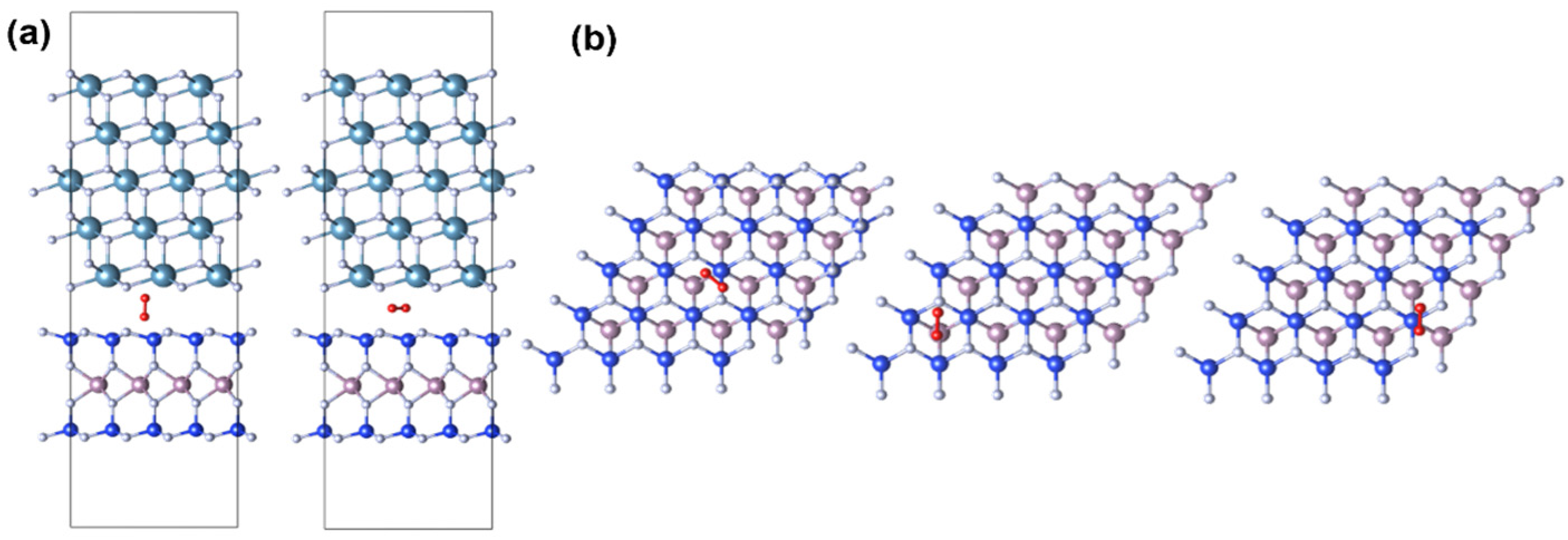
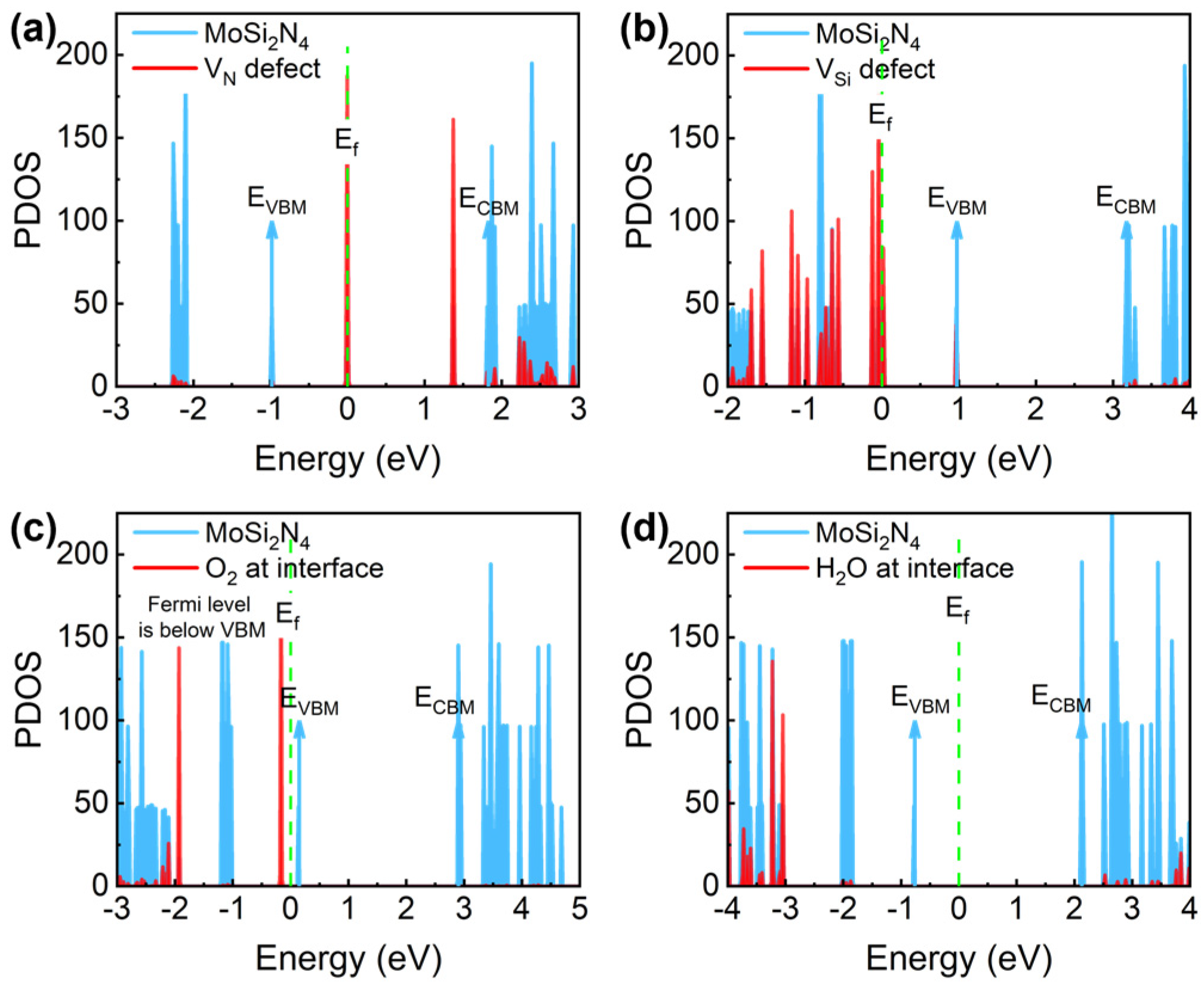
3.2. The Charge-Trapping Centers in CaF2-MoSi2N4

Now, we study the MoSi2N4-CaF2 system. MoSi2N4 is a 2D material with seven atomic layers. One Mo atomic layer lies in the middle while two Si-N-Si tri-layers lie on the top and bottom surfaces symmetrically. It can be seen that the VBM and CBM are provided by MoSi2N4 (Figure 7b), and the band offsets are greater than 2 eV, which makes charge tunneling difficult. Vacancy defects caused by the shedding of N atoms and Si (Figure 7a) atoms on the surface layer are the primary problems to be considered. At the same time, the influence of the adsorption of oxygen molecules and water molecules (Figure 7a) during device manufacture is also considered. The atoms highlighted in green in Figure 7a represent defects and adsorption sites.
For the N vacancy (VN) (Figure 8a), two defect levels are induced into the band gap, of which the half-occupied d1 state is 0.98 eV above VBM and the empty d2 state is 0.45 eV below CBM. Such small energy barriers make them very active hole/electron-trapping centers. In contrast, the VSi defect induces no defect levels close to the CBM, as is shown in Figure 8b, but it induces many defect levels below the VBM. Specifically, the electrons in VBM have spontaneously transferred to the defect sites, shifting the Fermi level below the VBM and making the CaF2-MoSi2N4 a whole p-type heterostructure. Interestingly, the adsorption of oxygen in the CaF2-MoSi2N4 interface has a very similar effect, as is shown in Figure 8c, the electrons in VBM are spontaneously captured by the oxygen, and the MoSi2N4 becomes a p-type material. If the oxygen density is high, the performance and reliability of the device will be greatly reduced. In comparison, the adsorption of water molecules in the interface does not have such an effect, as is shown in Figure 8d. The water-related defect energy level is far from the band edge of MoSi2N4. This further confirms that water molecule adsorption is less important than oxygen adsorption in impacting device performance and reliability. To present the importance of different defects more intuitively, Table 2 summarizes and compares the information of all defects in the CaF2-MoSi2N4 system.

4. Conclusions

In conclusion, we have investigated the various defects and adsorbates in CaF2-based 2D material MOSFET structures to distinguish their importance in degrading device performance and reliability. First, the intrinsic defects in channel materials, including the Vs. and VMo in MoS2, and VSi and VN in MoSi2N4, are very active charge-trapping centers. At the same time, although the intrinsic defect VMoS6 causes many defect states in the band gap, it is not a significant defect due to its large formation energy. Second, the adsorbed oxygen molecules in the channel/CaF2 interface or CaF2 surface are very important trap centers, and they can even spontaneously change the MoSi2N4 to p-type. Third, the adsorbed water molecules are inactive in capture charges, and thus, are much less important in affecting device performance. An elaborate table comparing the detailed properties of different defects is provided so that both experimental researchers and theorists can refer to it easily. Moreover, the intrinsic defect VSi in CaF2-MoSi2N4 can also lead to conversion to p-type transistors. Finally, we found that VF in CaF2 spontaneously contributes two electrons to CBM.
The significance of defects or adsorption in CaF2-based 2D material MOSFETs is not solely contingent upon the defect energy level; rather, it is also contingent upon the formation energy and transport type of the device. The two tables presented in the article provide a comprehensive demonstration of the impact of defects on performance. Furthermore, this methodology can facilitate the development of a system tool in the future, which will enable the determination of the impact of defects on device performance. Especially worth mentioning is the adsorption of oxygen molecules, which is a more problematic phenomenon than the adsorption of water molecules. To avoid this issue, it is advisable to isolate oxygen as much as possible during device preparation or use objects that do not introduce additional pollution sources to adsorb oxygen. These results mean that the exclusion of adsorbates in device fabrication is as important as growing high-quality channel material to obtain better device performance. The findings of our research can be extrapolated to the significance of different capture centers in a variety of 2D material MOSFETs.

Author Contributions

Conceptualization, Z.Z. and Y.-Y.L.; methodology, Z.Z. and Y.-Y.L.; formal analysis, Z.Z., J.G. and Y.-Y.L.; resources, J.G. and Y.-Y.L.; writing—original draft preparation, Z.Z.; writing—review and editing, T.X., J.G. and Y.-Y.L.; funding acquisition, J.G. and Y.-Y.L. All authors have read and agreed to the published version of the manuscript.

Funding

This research was funded by the National Natural Science Foundation of China (Grant No. 62174155 and No. T2293702), CAS Project for Young Scientists in Basic Research (No. YSBR-056), the Inner Mongolia Natural Science Foundation No. 2023ZD27, and the National Natural Science Foundation of China Grant No. 11964022.

Data Availability Statement

The data presented in this study are available on request from the corresponding author.

Acknowledgments

This work acknowledges the support from the School of Physical Science and Technology, Inner Mongolia University and Institute of semiconductors, Chinese Academy of Sciences.

Conflicts of Interest

The authors declare no conflicts of interest.

References

  1. Novoselov, K.S.; Geim, A.K.; Morozov, S.V.; Jiang, D.; Zhang, Y.; Dubonos, S.V.; Grigorieva, I.V.; Firsov, A.A. Electric Field Effect in Atomically Thin Carbon Films. Science 2004, 306, 666–669. [Google Scholar] [CrossRef] [PubMed]
  2. Novoselov, K.S.; Geim, A.K.; Morozov, S.V.; Jiang, D.; Katsnelson, M.I.; Grigorieva, I.V.; Dubonos, S.V.; Firsov, A.A. Two-Dimensional Gas of Massless Dirac Fermions in Graphene. Nature 2005, 438, 197–200. [Google Scholar] [CrossRef] [PubMed]
  3. Benka, S.G. Two-Dimensional Atomic Crystals. Proc. Natl. Acad. Sci. USA 2005, 102, 10451–10453. [Google Scholar] [CrossRef]
  4. Geim, A.K.; Novoselov, K.S. The Rise of Graphene. Nat. Mater. 2007, 6, 183–191. [Google Scholar] [CrossRef] [PubMed]
  5. Mak, K.F.; Lee, C.; Hone, J.; Shan, J.; Heinz, T.F. Atomically Thin MoS2: A New Direct-Gap Semiconductor. Phys. Rev. Lett. 2010, 105, 136805. [Google Scholar] [CrossRef] [PubMed]
  6. Radisavljevic, B.; Radenovic, A.; Brivio, J.; Giacometti, V.; Kis, A. Single-Layer MoS2 Transistors. Nat. Nanotechnol. 2011, 6, 147–150. [Google Scholar] [CrossRef] [PubMed]
  7. Li, L.; Yu, Y.; Ye, G.J.; Ge, Q.; Ou, X.; Wu, H.; Feng, D.; Chen, X.H.; Zhang, Y. Black Phosphorus Field-Effect Transistors. Nat. Nanotechnol. 2014, 9, 372–377. [Google Scholar] [CrossRef] [PubMed]
  8. Novoselov, K.S.; Mishchenko, A.; Carvalho, A.; Castro Neto, A.H. 2D Materials and van Der Waals Heterostructures. Science 2016, 353, aac9439. [Google Scholar] [CrossRef] [PubMed]
  9. Ortiz Balbuena, J.; Tutor De Ureta, P.; Rivera Ruiz, E.; Mellor Pita, S. Enfermedad de Vogt-Koyanagi-Harada. Med. Clin. 2016, 146, 93–94. [Google Scholar] [CrossRef]
  10. Wse, L.; Allain, A.; Kis, A. Terms of Use Electron and Hole Mobilities in Single-layer WSe2. ACS Nano 2014, 8, 7180–7185. [Google Scholar]
  11. Pan, Y.; Jia, K.; Huang, K.; Wu, Z.; Bai, G.; Yu, J.; Zhang, Z.; Zhang, Q.; Yin, H. Near-Ideal Subthreshold Swing MoS 2 Back-Gate Transistors with an Optimized Ultrathin HfO2 Dielectric Layer. Nanotechnology 2019, 30, 095202. [Google Scholar] [CrossRef] [PubMed]
  12. Bolshakov, P.; Zhao, P.; Azcatl, A.; Hurley, P.K.; Wallace, R.M.; Young, C.D. Improvement in Top-Gate MoS2 Transistor Performance Due to High Quality Backside Al2O3 Layer. Appl. Phys. Lett. 2017, 111, 032110. [Google Scholar] [CrossRef]
  13. Lee, C.; Rathi, S.; Khan, M.A.; Lim, D.; Kim, Y.; Yun, S.J.; Youn, D.H.; Watanabe, K.; Taniguchi, T.; Kim, G.H. Comparison of Trapped Charges and Hysteresis Behavior in HBN Encapsulated Single MoS2 Flake Based Field Effect Transistors on SiO2 and HBN Substrates. Nanotechnology 2018, 29, 335202. [Google Scholar] [CrossRef] [PubMed]
  14. Cassabois, G.; Valvin, P.; Gil, B. Hexagonal Boron Nitride Is an Indirect Bandgap Semiconductor. Nat. Photonics 2016, 10, 262–266. [Google Scholar] [CrossRef]
  15. Geick, R.; Perry, C.H.; Rupprecht, G. Normal Modes in Hexagonal Boron Nitride. Phys. Rev. 1966, 146, 543–547. [Google Scholar] [CrossRef]
  16. Illarionov, Y.Y.; Vexler, M.I.; Fedorov, V.V.; Suturin, S.M.; Sokolov, N.S. Electrical and Optical Characterization of Au/CaF2/p-Si(111) Tunnel-Injection Diodes. J. Appl. Phys. 2014, 115, 223706. [Google Scholar] [CrossRef]
  17. Usiskin, R.; Sigle, W.; Kelsch, M.; van Aken, P.A.; Maier, J. Ion Transport in Nanocrystalline CaF2 Films. J. Appl. Phys. 2021, 130, 105301. [Google Scholar] [CrossRef]
  18. Tyaginov, S.E.; Illarionov, Y.Y.; Vexler, M.I.; Bina, M.; Cervenka, J.; Franco, J.; Kaczer, B.; Grasser, T. Modeling of Deep-Submicron Silicon-Based MISFETs with Calcium Fluoride Dielectric. J. Comput. Electron. 2014, 13, 733–738. [Google Scholar] [CrossRef]
  19. Illarionov, Y.Y.; Banshchikov, A.G.; Polyushkin, D.K.; Wachter, S.; Knobloch, T.; Thesberg, M.; Mennel, L.; Paur, M.; Stöger-Pollach, M.; Steiger-Thirsfeld, A.; et al. Ultrathin Calcium Fluoride Insulators for Two-Dimensional Field-Effect Transistors. Nat. Electron. 2019, 2, 230–235. [Google Scholar] [CrossRef]
  20. Foster, A.S.; Trevethan, T.; Shluger, A.L. Structure and Diffusion of Intrinsic Defects, Adsorbed Hydrogen, and Water Molecules at the Surface of Alkali-Earth Fluorides Calculated Using Density Functional Theory. Phys. Rev. B Condens. Matter Mater. Phys. 2009, 80, 115421. [Google Scholar] [CrossRef]
  21. Song, H.; Zhou, F.; Yan, S.; Su, X.; Wu, H.; Wu, Q.; Gao, Y.; Chen, R.; Chen, T.; Yao, J.; et al. Enhanced Transport and Optoelectronic Properties of van Der Waals Materials on CaF2 Films. Nano Lett. 2023, 23, 4983–4990. [Google Scholar] [CrossRef] [PubMed]
  22. Wen, C.; Banshchikov, A.G.; Illarionov, Y.Y.; Frammelsberger, W.; Knobloch, T.; Hui, F.; Sokolov, N.S.; Grasser, T.; Lanza, M. Dielectric Properties of Ultrathin CaF2 Ionic Crystals. Adv. Mater. 2020, 32, e2002525. [Google Scholar] [CrossRef] [PubMed]
  23. Huang, L.; Liu, H.; Cui, W. High-k Monolayer CaF2 as the Gate Dielectric for Two-Dimensional SiC-Based Field-Effect Transistors. ACS Appl. Electron. Mater. 2023, 5, 5082–5092. [Google Scholar] [CrossRef]
  24. Vishwanath, S.; Liu, X.; Rouvimov, S.; Mende, P.C.; Azcatl, A.; McDonnell, S.; Wallace, R.M.; Feenstra, R.M.; Furdyna, J.K.; Jena, D.; et al. Comprehensive Structural and Optical Characterization of MBE Grown MoSe2 on Graphite, CaF2 and Graphene. 2D Mater. 2015, 2, 024007. [Google Scholar] [CrossRef]
  25. Wen, C.; Lanza, M. Calcium Fluoride as High-k Dielectric for 2D Electronics. Appl. Phys. Rev. 2021, 8, 021307. [Google Scholar] [CrossRef]
  26. Grasser, T.; Kaczer, B.; Goes, W.; Reisinger, H.; Aichinger, T.; Hehenberger, P.; Wagner, P.J.; Schanovsky, F.; Franco, J.; Toledano Luque, M.; et al. The Paradigm Shift in Understanding the Bias Temperature Instability: From Reaction-Diffusion to Switching Oxide Traps. IEEE Trans. Electron Devices 2011, 58, 3652–3666. [Google Scholar] [CrossRef]
  27. Guo, Y.; Wei, X.; Shu, J.; Liu, B.; Yin, J.; Guan, C.; Han, Y.; Gao, S.; Chen, Q. Charge Trapping at the MoS2-SiO2 Interface and Its Effects on the Characteristics of MoS2 Metal-Oxide-Semiconductor Field Effect Transistors. Appl. Phys. Lett. 2015, 106, 103109. [Google Scholar] [CrossRef]
  28. Illarionov, Y.Y.; Waltl, M.; Bartolomeo, A.D.; Genovese, L.; Illarionov, Y.Y.; Rzepa, G.; Waltl, M.; Knobloch, T.; Grill, A. The Role of Charge Trapping in MoS2/SiO2 and MoS2/HBN Field-Effect Transistors. 2D Mater. 2016, 3, 035004. [Google Scholar] [CrossRef]
  29. Di Bartolomeo, A.; Genovese, L.; Giubileo, F.; Iemmo, L.; Luongo, G.; Foller, T.; Schleberger, M. Hysteresis in the Transfer Characteristics of MoS2 Transistors. 2D Mater. 2018, 5, 015014. [Google Scholar] [CrossRef]
  30. Late, D.J.; Liu, B.; Matte, H.S.S.R.; Dravid, V.P.; Rao, C.N.R. Hysteresis in Single-Layer MoS2 Field Effect Transistors. ACS Nano 2012, 6, 5635–5641. [Google Scholar] [CrossRef]
  31. Park, Y.; Baac, H.W.; Heo, J.; Yoo, G. Thermally Activated Trap Charges Responsible for Hysteresis in Multilayer MoS2 Field-Effect Transistors. Appl. Phys. Lett. 2016, 108, 083102. [Google Scholar] [CrossRef]
  32. Ma, X.; Liu, Y.Y.; Zeng, L.; Chen, J.; Wang, R.; Wang, L.W.; Wu, Y.; Jiang, X. Defects Induced Charge Trapping/Detrapping and Hysteresis Phenomenon in MoS2 Field-Effect Transistors: Mechanism Revealed by Anharmonic Marcus Charge Transfer Theory. ACS Appl. Mater. Interfaces 2022, 14, 2185–2193. [Google Scholar] [CrossRef]
  33. Xiong, T.; Yang, J.; Deng, H.-X.; Wei, Z.; Liu, Y.-Y. The Mechanism of Improving Germanium Metal–Oxide–Semiconductor Field-Effect Transistors’ Reliability by High-k Dielectric and Yttrium-Doping: From the View of Charge Trapping. J. Appl. Phys. 2022, 132, 174506. [Google Scholar] [CrossRef]
  34. Liu, Y.Y.; Liu, F.; Wang, R.; Luo, J.W.; Jiang, X.; Huang, R.; Li, S.S.; Wang, L.W. Characterizing the Charge Trapping across Crystalline and Amorphous Si/SiO2/HfO2 Stacks from First-Principle Calculations. Phys. Rev. Appl. 2019, 12, 064012. [Google Scholar] [CrossRef]
  35. Liu, Y.Y.; Zheng, F.; Jiang, X.; Luo, J.W.; Li, S.S.; Wang, L.W. Ab Initio Investigation of Charge Trapping Across the Crystalline- Si -Amorphous- SiO2 Interface. Phys. Rev. Appl. 2019, 11, 044058. [Google Scholar] [CrossRef]
  36. Liu, Y.Y.; Jiang, X. Physics of Hole Trapping Process in High-k Gate Stacks: A Direct Simulation Formalism for the Whole Interface System Combining Density-Functional Theory and Marcus Theory. In Proceedings of the 2018 IEEE International Electron Devices Meeting (IEDM), San Francisco, CA, USA, 1–5 December 2018. [Google Scholar] [CrossRef]
  37. Illarionov, Y.Y.; Knobloch, T.; Uzlu, B.; Banshchikov, A.G.; Ivanov, I.A.; Sverdlov, V.; Otto, M.; Stoll, S.L.; Vexler, M.I.; Waltl, M.; et al. Variability and High Temperature Reliability of Graphene Field-Effect Transistors with Thin Epitaxial CaF2 Insulators. npj 2D Mater. Appl. 2024, 8, 1–10. [Google Scholar] [CrossRef]
  38. Durante, O.; Intonti, K.; Viscardi, L.; De Stefano, S.; Faella, E.; Kumar, A.; Pelella, A.; Romeo, F.; Giubileo, F.; Alghamdi, M.S.G.; et al. Subthreshold Current Suppression in ReS2 Nanosheet-Based Field-Effect Transistors at High Temperatures. ACS Appl. Nano Mater. 2023, 6, 21663–21670. [Google Scholar] [CrossRef] [PubMed]
  39. Ishibe, T.; Tomeda, A.; Komatsubara, Y.; Kitaura, R.; Uenuma, M.; Uraoka, Y.; Yamashita, Y.; Nakamura, Y. Carrier and Phonon Transport Control by Domain Engineering for High-Performance Transparent Thin Film Thermoelectric Generator. Appl. Phys. Lett. 2021, 118, 151601. [Google Scholar] [CrossRef]
  40. Xia, J.; Sohail, M.; Nazeeruddin, M.K. Efficient and Stable Perovskite Solar Cells by Tailoring of Interfaces. Adv. Mater. 2023, 35, e2211324. [Google Scholar] [CrossRef]
  41. Li, Z.; Baskurt, M.; Sahin, H.; Gao, S.; Kang, J. Electronic Properties of Intrinsic Vacancies in Single-Layer CaF2 and Its Heterostructure with Monolayer MoS2. J. Appl. Phys. 2021, 130, 055301. [Google Scholar] [CrossRef]
  42. Zhang, H.; Shi, B.; Xu, L.; Yan, J.; Zhao, W.; Zhang, Z.; Zhang, Z.; Lu, J. Sub-5 Nm Monolayer MoS2 Transistors toward Low-Power Devices. ACS Appl. Electron. Mater. 2021, 3, 1560–1571. [Google Scholar] [CrossRef]
  43. Hua, Q.; Gao, G.; Jiang, C.; Yu, J.; Sun, J.; Zhang, T.; Gao, B.; Cheng, W.; Liang, R.; Qian, H.; et al. Atomic Threshold-Switching Enabled MoS2 Transistors towards Ultralow-Power Electronics. Nat. Commun. 2020, 11, 6207. [Google Scholar] [CrossRef] [PubMed]
  44. Huang, B.; Li, N.; Wang, Q.; Ouyang, C.; He, C.; Zhang, L.; Du, L.; Yang, W.; Yang, R.; Shi, D.; et al. Optoelectronic Synapses Based on MoS2 Transistors for Accurate Image Recognition. Adv. Mater. Interfaces 2022, 9, 2201558. [Google Scholar] [CrossRef]
  45. Di Bartolomeo, A.; Kumar, A.; Durante, O.; Sessa, A.; Faella, E.; Viscardi, L.; Intonti, K.; Giubileo, F.; Martucciello, N.; Romano, P.; et al. Temperature-Dependent Photoconductivity in Two-Dimensional MoS2 Transistors. Mater. Today Nano 2023, 24, 100382. [Google Scholar] [CrossRef]
  46. Hong, Y.L.; Liu, Z.; Wang, L.; Zhou, T.; Ma, W.; Xu, C.; Feng, S.; Chen, L.; Chen, M.L.; Sun, D.M.; et al. Chemical Vapor Deposition of Layered Two-Dimensional MoSi2N4 Materials. Science 2020, 369, 670–674. [Google Scholar] [CrossRef] [PubMed]
  47. Zhao, P.; Jiang, Z.Y.; Zheng, J.M.; Lin, Y.M.; Du, A. Theoretical Study of a Novel WSi2N4/MoSi2N4 Heterostructure with Ultrafast Carrier Transport. J. Phys. Chem. C 2022, 126, 11380–11388. [Google Scholar] [CrossRef]
  48. Mortazavi, B.; Javvaji, B.; Shojaei, F.; Rabczuk, T.; Shapeev, A.V.; Zhuang, X. Exceptional Piezoelectricity, High Thermal Conductivity and Stiffness and Promising Photocatalysis in Two-Dimensional MoSi2N4 Family Confirmed by First-Principles. Nano Energy 2021, 82, 105716. [Google Scholar] [CrossRef]
  49. Yang, J.-S.; Zhao, L.; LI, S.-Q.; Liu, H.; Wang, L.; Chen, M.; Gao, J.; Zhao, J. Accurate Electronic Properties and Non-Linear Optical Response of Two-Dimensional MA2Z4. Nanoscale 2021, 13, 5479–5488. [Google Scholar] [CrossRef]
  50. Jia, W.; Fu, J.; Cao, Z.; Wang, L.; Chi, X.; Gao, W.; Wang, L.W. Fast Plane Wave Density Functional Theory Molecular Dynamics Calculations on Multi-GPU Machines. J. Comput. Phys. 2013, 251, 102–115. [Google Scholar] [CrossRef]
  51. Jia, W.; Cao, Z.; Wang, L.; Fu, J.; Chi, X.; Gao, W.; Wang, L.W. The Analysis of a Plane Wave Pseudopotential Density Functional Theory Code on a GPU Machine. Comput. Phys. Commun. 2013, 184, 9–18. [Google Scholar] [CrossRef]
  52. Hamann, D.R. Optimized Norm-Conserving Vanderbilt Pseudopotentials. Phys. Rev. B Condens. Matter Mater. Phys. 2013, 88, 085117. [Google Scholar] [CrossRef]
  53. Heyd, J.; Peralta, J.E.; Scuseria, G.E.; Martin, R.L. Energy Band Gaps and Lattice Parameters Evaluated with the Heyd-Scuseria-Ernzerhof Screened Hybrid Functional. J. Chem. Phys. 2005, 123, 174101. [Google Scholar] [CrossRef] [PubMed]
  54. Grimme, S.; Antony, J.; Ehrlich, S.; Krieg, H. A Consistent and Accurate Ab Initio Parametrization of Density Functional Dispersion Correction (DFT-D) for the 94 Elements H-Pu. J. Chem. Phys. 2010, 132, 154104–154119. [Google Scholar] [CrossRef] [PubMed]
  55. Chen, J.; Zhang, Z.; Guo, Y.; Robertson, J. Electronic Properties of CaF2 bulk and Interfaces. J. Appl. Phys. 2022, 131, 215302. [Google Scholar] [CrossRef]
  56. Zhou, W.; Zou, X.; Najmaei, S.; Liu, Z.; Shi, Y.; Kong, J.; Lou, J.; Ajayan, P.M.; Yakobson, B.I.; Idrobo, J.C. Intrinsic Structural Defects in Monolayer Molybdenum Disulfide. Nano Lett. 2013, 13, 2615–2622. [Google Scholar] [CrossRef] [PubMed]
  57. Robertson, J.; Falabretti, B. Band Offsets of High K Gate Oxides on III-V Semiconductors. J. Appl. Phys. 2006, 100, 014111. [Google Scholar] [CrossRef]
  58. Robertson, J. Band Offsets, Schottky Barrier Heights, and Their Effects on Electronic Devices. J. Vac. Sci. Technol. A Vacuum Surfaces Film. 2013, 31, 050821. [Google Scholar] [CrossRef]
  59. Robertson, J. Band Offsets of Wide-Band-Gap Oxides and Implications for Future Electronic Devices. J. Vac. Sci. Technol. B Microelectron. Nanometer Struct. 2000, 18, 1785. [Google Scholar] [CrossRef]
Figure 1. Flowchart of calculation method.
Nanomaterials 14 01038 g001
Figure 2. Atomic structure and type-I band alignment of CaF2-MoS2 interface models. (a) Atomic structure of 5-layer CaF2 and 2-layer MoS2, as well as (b) band alignment along the Z-axis direction.
Nanomaterials 14 01038 g002
Figure 3. The position of the F vacancy (VF) defect energy level in the CaF2 band. The blue, green, and red lines represent the PDOS of CaF2, MoS2, and VF, respectively.
Nanomaterials 14 01038 g003
Figure 4. The energy level distribution of different defects. (a) S vacancy (VS), (b) Mo vacancy (VMo), (c) MoS3 vacancy (VMoS3), and (d) MoS6 vacancy (VMoS6).
Nanomaterials 14 01038 g004
Figure 5. The energy level distribution of different molecules adsorbed on the surface and interface of CaF2-MoS2.
Nanomaterials 14 01038 g005
Figure 6. Different situations of O2 adsorption. (a) Compare O2 perpendicular/parallel to the interface; (b) compare different adsorption positions.
Nanomaterials 14 01038 g006
Figure 7. Atomic structure and type-I band alignment of CaF2-MoS2 interface models. (a,b) The atomic structure of 5-layer CaF2, and 1-layer MoSi2N4, as well as the band alignment along the Z-axis direction.
Nanomaterials 14 01038 g007
Figure 8. The energy level distribution of different molecules adsorbed on the surface and interface of CaF2-MoS2. (a) N vacancy (VN), (b) Si vacancy (VSi), (c) O2 at interface, and (d) H2O at interface.
Nanomaterials 14 01038 g008
Table 1. Importance of different trapping centers in CaF2-MoS2.
Defect
Types
Defect
State
ΔE-
VBM
(eV)
ΔE-
CBM
(eV)
n-FET
Importance
p-FET
Importance
Fromation Energy (eV)Overall
Importance
VSd1−0.38−1.912.91
d20.95−0.57
VMod1−0.06−1.638.52
d20.40−1.17
d30.71−0.86
VMoS3d1−0.25−1.7811.81
d20.89−0.64
d30.99−0.53
VMoS6type1<0.50>1.5021.41
type2<1.00>1.00
type3>1.75<0.25
O2 at interfaced1−0.99−2.450.68
d2−0.55−2.00
d3−0.85−2.31
H2O at interface −3.42−4.910.61
O2 in MoS2 −0.37−2.012.35
O2 at surface 1.11−0.412.25
Table 2. Importance of different capture centers in CaF2-MoSi2N4.
Defect
Types
Defect
State
ΔE-
VBM
(eV)
ΔE-
CBM
(eV)
n-FET
Importance
p-FET
Importance
Fromation
Energy (eV)
Overall
Importance
VNd10.98−1.835.97
d22.36−0.45
VSid1−1.01−3.2311.15
d20.00−2.22
O2 at interface −0.32−3.070.19
H2O at interface −2.29−5.170.34
Disclaimer/Publisher’s Note: The statements, opinions and data contained in all publications are solely those of the individual author(s) and contributor(s) and not of MDPI and/or the editor(s). MDPI and/or the editor(s) disclaim responsibility for any injury to people or property resulting from any ideas, methods, instructions or products referred to in the content.

