Article

Optimization of Thermoelectric Nanoantenna for Massive High-Output-Voltage Arrays

by
Mohamad Khoirul Anam
1,
Yudhistira Yudhistira
2 and
Sangjo Choi
2,*
1
Research Center for Testing Technology and Standard, National Research and Innovation Agency (BRIN), South Tangerang 15314, Indonesia
2
School of Electronics Engineering, Kyungpook National University, Daegu 41566, Republic of Korea
*
Author to whom correspondence should be addressed.
Nanomaterials 2024, 14(13), 1159; https://doi.org/10.3390/nano14131159
Submission received: 2 June 2024 / Revised: 3 July 2024 / Accepted: 4 July 2024 / Published: 7 July 2024

Abstract

:
Thermoelectric nanoantennas have been extensively investigated due to their ability to directly convert infrared (IR) radiation into direct current without an additional rectification device. In this study, we introduce a thermoelectric nanoantenna geometry for maximum output voltage (Voc) and propose an optimal series array configuration with a finite number of antennas to enhance the Voc. A finite and open-ended SiO2 substrate, with a thickness of a quarter-effective wavelength at a frequency of 28.3 THz, is used to generate standing waves within the substrate. An array of antennas is then positioned optimally on the substrate to maximize the temperature difference ( T ) between hot and cold areas, thereby increasing the average Voc per antenna element. In numerical simulations, a linearly polarized incident wave with a power density of 1.42 W/cm2 is applied to the structure. The results show that a single antenna with the optimum geometry on a substrate measuring 35 µm × 35 µm generates a T of 64.89 mK, corresponding to a Voc of 1.75 µV. Finally, a series array of 5 × 6 thermoelectric nanoantennas on a 150 µm × 75 µm substrate including measurement pads achieves an average T of 49.60 mK with a total Voc of 40.18 µV, resulting in an average Voc of 1.34 µV per antenna element and a voltage responsivity (βv) of 0.77 V/W. This value, achieved solely by optimizing the antenna geometry and open-ended substrate, matches or exceeds the Voc and βv of approximately 1 µV and 0.66 V/W, respectively, from suspended thermoelectric antenna arrays over air cavities. Therefore, the proposed thermoelectric nanoantenna array device, characterized by high stability and ease of fabrication, is suitable for manufacturing massive nanoantenna arrays for high-output IR-DC energy harvesters.

1. Introduction

Infrared (IR) radiation emitted by artificial sources such as heating devices covers a wide range of IR wavelengths. However, a large portion of this IR energy is typically unused as thermal waste energy [1,2,3]. This has motivated the development of systems for capturing IR waste energy and converting it into another form of energy, such as electricity. Among various methods, thermoelectric nanoantennas represent highly cost-effective devices for directly converting IR radiation into electricity without requiring additional rectification devices such as metal–insulator–metal and metal–oxide–semiconductor-based nanoantennas [4,5].
Generally, the antenna structure in thermoelectric devices consists of a dipole nanoantenna as an efficient receiver for capturing external IR radiation. The center of this nanoantenna is connected with a nano-thermocouple that converts the captured IR radiation into an open-circuit voltage (Voc). The electrical length of the nanoantenna typically matches the half-effective wavelength of the incident IR wave, resulting in a strong current at the center [6,7,8]. This current increases the antenna temperature at its center due to the kinetic energy from interactions between charge carriers and quasi-particles from the antenna element [9,10,11,12]. The resulting temperature gradient causes the thermally excited electrons from the antenna to travel with higher energy along the nano-thermocouple, resulting in the generation of Voc [13]. The Voc can be calculated by multiplying the relative Seebeck coefficient (ΔS) of the nano-thermocouple and the temperature difference between hot and cold areas (ΔT) [14,15,16]. Although materials such as telluride-based materials and carbon nanotubes with high Seebeck coefficients can be used for the thermocouple in the thermoelectric nanoantenna design, we aimed to find the optimum nanoantenna using a metal-based thermocouple [17,18,19].
Thermoelectric nanoantennas with metal-based thermocouples mounted on a grounded substrate were used for IR-DC conversion [20,21]. However, this structure provided a low Voc as only one antenna element contributed to the total Voc. To achieve a higher Voc, several thermoelectric nanoantennas were electrically connected in series [20,22,23,24]. Specifically, an array concept was realized using a series connection of dipole-shaped nanoantennas integrated with a single metal thermocouple composed of Ni, achieving a Voc of 3.25 µV with a ∆T of 15.5 mK between the hot and cold junctions [22]. Although this structure incorporated a large number (>400) of nanoantennas coupled with thermocouples, the average Voc per antenna element (7.38 nV) was too low due to a small Seebeck coefficient difference associated with the single metal thermocouple.
To increase the average Voc, researchers have proposed a nanoantenna array structure combined with a bimetal thermocouple to achieve a higher Seebeck coefficient difference. For example, Szakmany et al. designed a dipole nanoantenna array combined with a bimetal thermocouple (Au-Pd), achieving an improved average Voc of 0.12 µV due to the higher difference in the Seebeck coefficient [20]. The Voc was further improved by designing an antenna array structure on a thermally insulated area to prevent heat transfer from the antenna center [23,25,26]. To implement this concept, Szakmany et al. suspended a large array of thermoelectric nanoantennas (>200 elements) in a series connection over an air-filled cavity, resulting in a Voc of 200 µV, with an average Voc of 1 µV per antenna [23]. However, the use of a single metal thermocouple with a low Seebeck coefficient difference limited the Voc, despite a high temperature difference in the array. Bimetal versions of similar air-cavity-based arrays with 48 antennas have been reported, but only the relative differences in Voc depending on the atmospheric pressure, without absolute Voc levels from the arrays, were presented [27]. To the best of the authors’ knowledge, a single antenna utilizing a bimetal thermocouple and an air-cavity demonstrated a high Voc of 38 µV, but such a high Voc per antenna from its array has not yet been reported [21]. Recently, Anam et al. designed a bimetal thermoelectric nanoantenna on a grounded and open-ended SiO2 substrate with a quarter-wavelength thickness and increased the Voc to 2 µV [28]. The SiO2 substrate acted as a cavity and maximized the field at the antenna center through standing waves launched inside the substrate [28]. This device geometry was also more durable than air-cavity-based nanoantennas. Therefore, it is worthwhile to investigate the optimum thermoelectric nanoantenna geometry on a SiO2-based cavity and its array design to maximize the Voc from thermoelectric nanoantenna devices.
In this study, we investigated the optimal geometry for a bimetal thermoelectric nanoantenna to achieve the maximum Voc by optimizing the coupling between the antenna’s electric field and the standing wave in a grounded and open-ended SiO2 cavity. Based on the optimum single antenna geometry, we designed nanoantenna array structures, optimizing the vertical and horizontal distances between the antennas to maximize the Voc. Using these optimum distances, a 5 × 6 thermoelectric nanoantenna array structure achieved a Voc of 40.18 µV, with an average Voc of 1.31 µV per antenna and a voltage responsivity (βv) of 0.77 V/W. The increased average Voc was attributed to the enhanced field at the antenna elements due to the standing wave in the SiO2 cavity. The average Voc and βv were higher than the Voc of 1 µV per antenna and βv of 0.66 V/W from the existing thermoelectric nanoantenna array suspended over an air cavity [23]. The proposed thermoelectric nanoantenna array structure mounted on the SiO2 cavity provided a superior Voc and greater fabrication stability, rendering it promising for the development of high-output IR-energy-harvesting devices or sensors.

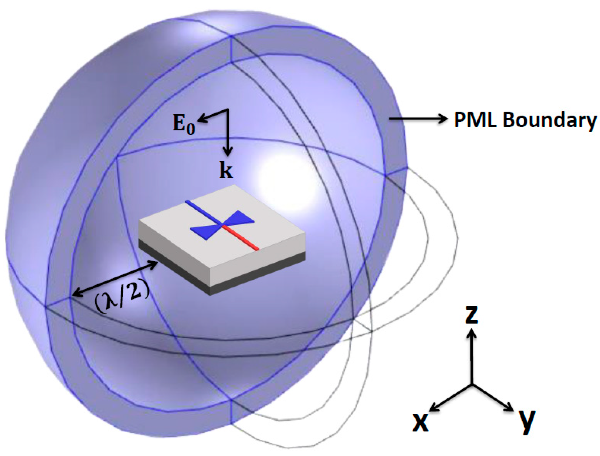
2. Simulation Methods

A numerical study was conducted to calculate the current density and temperature difference ( T) between the hot and cold junctions of a thermoelectric nanoantenna using heat transfer modules in COMSOL Multiphysics 5.0. Ti and Ni were used as metallic traces for the antenna and thermocouple, respectively. SiO2 and Al were used for the substrate and reflector, respectively. The relative permittivity ( ε ) and conductivity ( σ ) of the materials in the far IR region were calculated as ε = n 2 k 2 and σ = ε 0 × ε 2 × ω , respectively. Here, n and k denote the real and imaginary parts of the refractive index, respectively; and ε 0 ,   ε 2 , and ω are the vacuum permittivity, the imaginary part of the relative permittivity, and the angular frequency, respectively [29,30,31]. For heat transfer calculations, the thermal conductivity, heat capacity, and mass density were extracted from a previous study [32]. Overall, the scope of the simulation was based on microscopic or continuum-level properties of the materials instead of atomistic modeling including the topological heterostructure in the nanoantenna structure [33]. Although the junctions between the thermocouple and the nanoantenna could be analyzed more accurately by atomistic modeling, this was beyond the scope of this study.
In the simulation, the device was illuminated by a linearly polarized plane wave propagating along the negative z-direction, with the simulation boundary set by a perfectly matched layer (PML) with a thickness of ( λ / 2 ) to absorb outgoing waves without reflection, as shown in Figure 1. The vector component of the incident electric field (E0) with a power density of 1.42 W/cm2 was aligned with the antenna axis for the highest current excitation at the antenna center. To calculate the temperature difference (ΔT), heat transfer analysis was used by employing a convective boundary condition with a heat transfer coefficient of 5 W/m2·K from metal to free space [34]. The ΔT of the structure was calculated using ΔT = ThotTcold, where Thot and Tcold are the temperatures at the hot and cold junctions, located at the antenna center and ends of the nano-thermocouple, respectively. Finally, using the Seebeck coefficients of Ti (STi) and Ni (SNi) of 7.19 and −19.5 µV/K [35], respectively, ΔT was translated into Voc using ΔS × ΔT, where ΔS is STiSNi, the Seebeck coefficient difference between Ti and Ni [36]. It is noted that the ΔS of the bimetal junction in the thermocouple can vary compared to the values from their bulk materials due to the nanometer dimensions [37,38,39]. In simulations, the bulk values were used based on the reported measured data where a Pd-Ni junction of 75 nm2 using Ni showed a similar ΔS compared to the bulk value, and a Ti-Ni-junction-coupled nanoantenna demonstrated good agreement between the measured Voc and the simulated values using bulk Seebeck coefficients [28,38]. Nevertheless, the direct experimental verification of ΔS for the nanometer Ti-Ni junction will be worth investigating.

3. Results and Discussion

First, we investigated the optimal geometry for a single thermoelectric nanoantenna to achieve the maximum Voc in a given substrate. Using this optimal geometry, we arranged the antennas into a finite-series array structure to enhance the Voc. To this end, we tuned the array parameter, such as the nano-thermocouple length (Lt), antenna pitch size (P), and distance from the antenna to the substrate boundary (G) of the antennas in a finite SiO2 substrate. Finally, a 5 × 6 finite array with 30 antennas was designed using the optimum array parameters, and the device’s Voc and βv were calculated and analyzed.

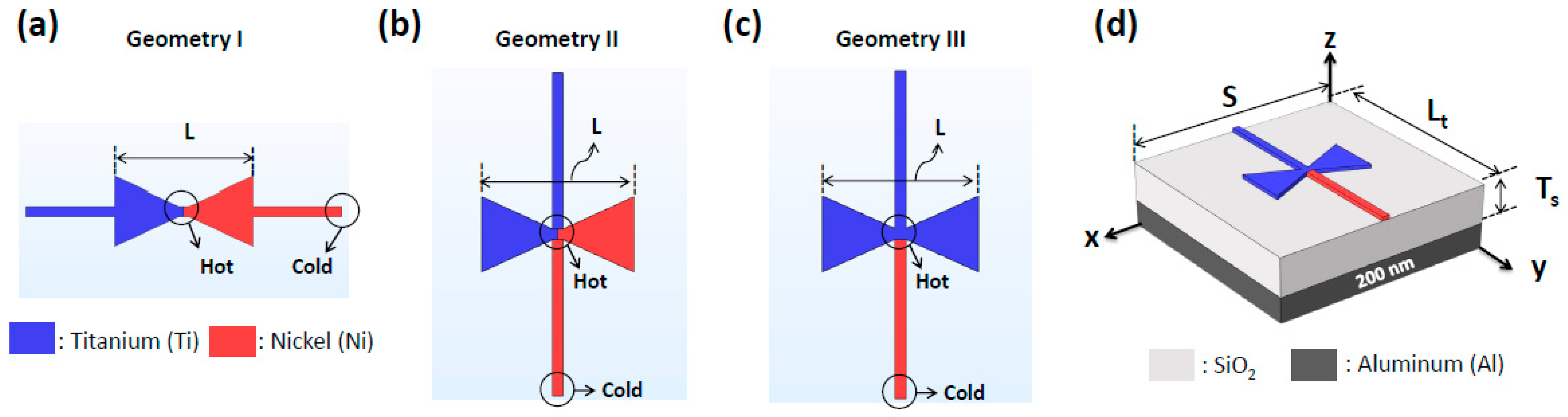
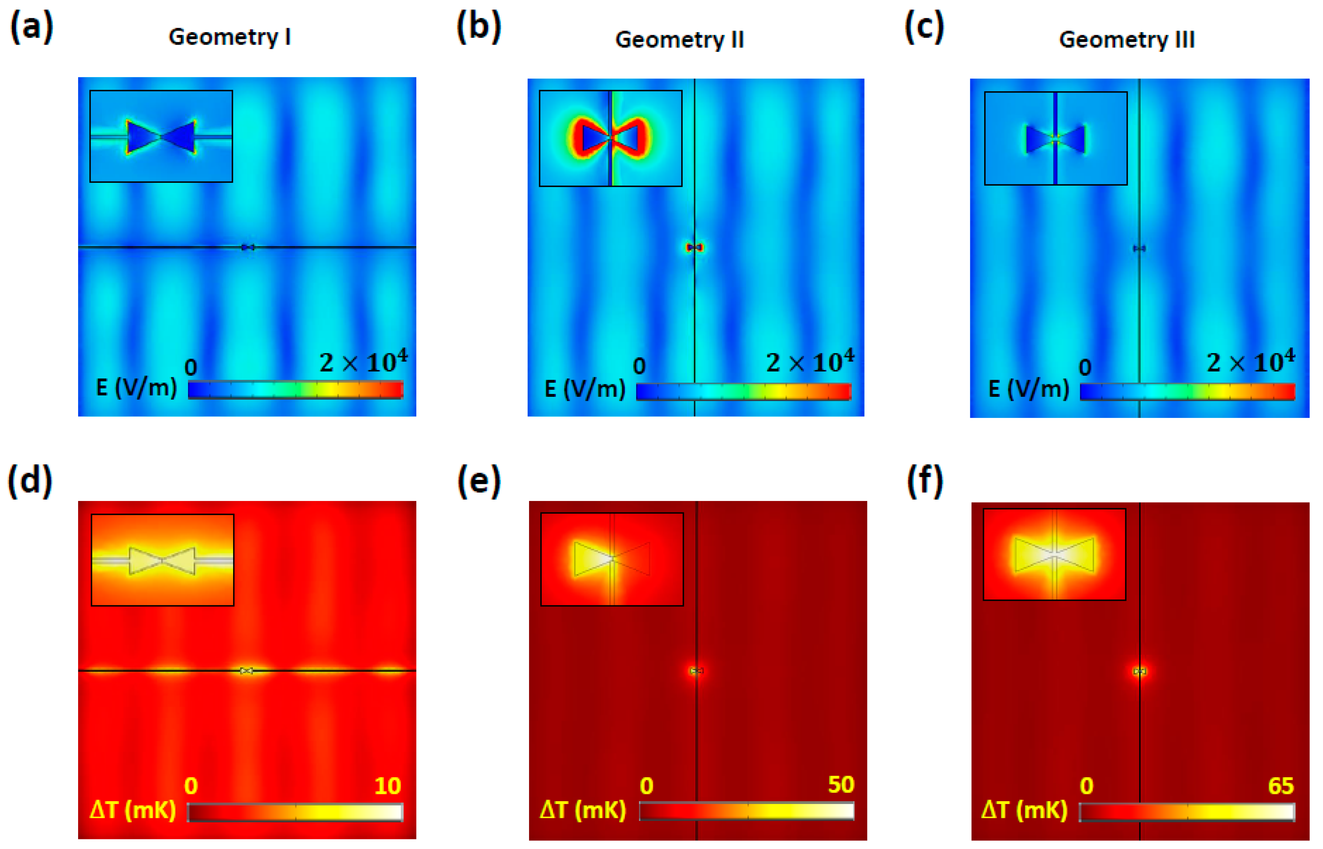
3.1. Optimization of Single Thermoelectric Nanoantenna Geometry

First, a single antenna was designed to achieve a high ΔT at a resonant frequency of 28.3 THz (wavelength of 10.6 µm). We used a bowtie-shaped nanoantenna to capture IR radiation instead of a dipole-shaped nanoantenna due to its larger effective area, resulting in a higher current at the antenna center. A pair of bimetal Ni-Ti was chosen as a nano-thermocouple to convert the ΔT into Voc. Three thermoelectric nanoantenna geometries were devised, as shown in Figure 2a–c, with the hot and cold junctions located at the antenna center and ends of the nano-thermocouple, respectively. In geometry I, the nano-thermocouple was connected to the middle of the two ends of the bimetal (Ni-Ti) bowtie nanoantenna in parallel. In geometry II, the same bimetal nanoantenna and thermocouple were used, but they were connected perpendicularly at the center of the bowtie structure. Geometry III was similar to geometry II with the antenna changed to a single metal (Ti) bowtie antenna [28]. In the implementation, the antenna was directly mounted on top of an open-ended SiO2 substrate backed with an Al reflector, as shown in Figure 2d. In all the geometries, the antenna length (L) was set as 1225 nm for resonance at 28.3 THz, and the substrate size (S) was set as 35 μm, supporting the TM40 mode in the substrate for constructive coupling at the antenna center [28]. The length (Lt) and width of the thermocouple were set as 35 μm and 70 nm, respectively, and the thickness of all the metallic structures, including the antenna and thermocouple, was 60 nm. The thickness (Ts) of the SiO2 substrate was set as 1.2 µm, a quarter of the effective wavelength inside SiO2 to achieve constructive coupling between the incident and reflected waves at the antenna. Lastly, a 200 nm thick Al reflector, considerably thicker than the skin depth of Al at 28.3 THz and fabricable using a conventional e-beam evaporation method, was used to perfectly reflect the incident wave without any leakage [28].
To determine the optimal antenna geometry for the highest Voc, we calculated the electric field and temperature distribution on the x–y plane in the middle of the antennas. Figure 3a–c show the electric field distribution with magnified views near the antennas (insets). In all cases, standing waves with maximum magnitude at the center of the substrate were generated due to the finite-sized and open-ended SiO2. In Figure 3a, the inset shows that the electric field of geometry I was distributed between the antenna and thermocouple because the ends of the antenna were connected to the thermocouple in parallel. Strong fields at the sharp tips of the antenna indicated that resonance from the antenna length was only maintained at small spots. This parallel connection between the antenna and thermocouple could not effectively confine and boost the fields near the thermocouple junction located at the antenna center. In contrast, as shown in Figure 3b,c, the antennas perpendicularly connected to the thermocouple at the antenna center exhibited considerably stronger fields near the antenna center. In both cases, the resonance from the finite-sized antenna was less perturbed compared with that of geometry I. In Figure 3b, representing geometry II, the highest field was observed near the antenna, likely due to the higher conductivity of Ni compared with Ti used in geometry III.
Figure 3d–f show the temperature distribution on the xy plane for the three geometries. In geometry I, the distributed field along the antenna and thermocouple caused heat to spread from the antenna to the thermocouple, reducing the ΔT between the hot and cold junctions, as shown in Figure 3d. Figure 3e shows that geometry II maintained a T reaching up to 50 mK, due to the higher electric fields near the antenna. However, the bowtie arm with Ni exhibited a much lower temperature, attributable to its higher thermal conductivity compared with that of Ti. Lastly, geometry III exhibited the highest T approaching 65 mK, despite having lower fields near the antenna compared with geometry II. This highest temperature in geometry III can be attributed to the lower thermal connectivity of Ti. In conclusion, to maximize the Voc of a thermoelectric antenna integrated with a bimetal (Ni-Ti) thermocouple, the construction of a single metal (Ti) nanoantenna with lower electrical and thermal conductivity between two metals (Ni and Ti) and its perpendicular connection to the bimetal thermocouple are necessary.
Figure 4a shows the ΔT of the three geometries of the single thermoelectric nanoantenna as a function of frequency. Geometry III provided the highest ΔT of 64.89 mK at 28.3 THz, followed by geometry II and geometry I, with values of 44.51 mK and 8.65 mK, respectively. Figure 4b illustrates that the Voc values of the three geometries were directly proportional to ΔT, with geometry III providing the maximum Voc of 1.75 µV at 28.3 THz. Based on the simulation results, geometry III was chosen for array designs to achieve the highest Voc, as discussed in the following sections.

3.2. Finite Array Structure

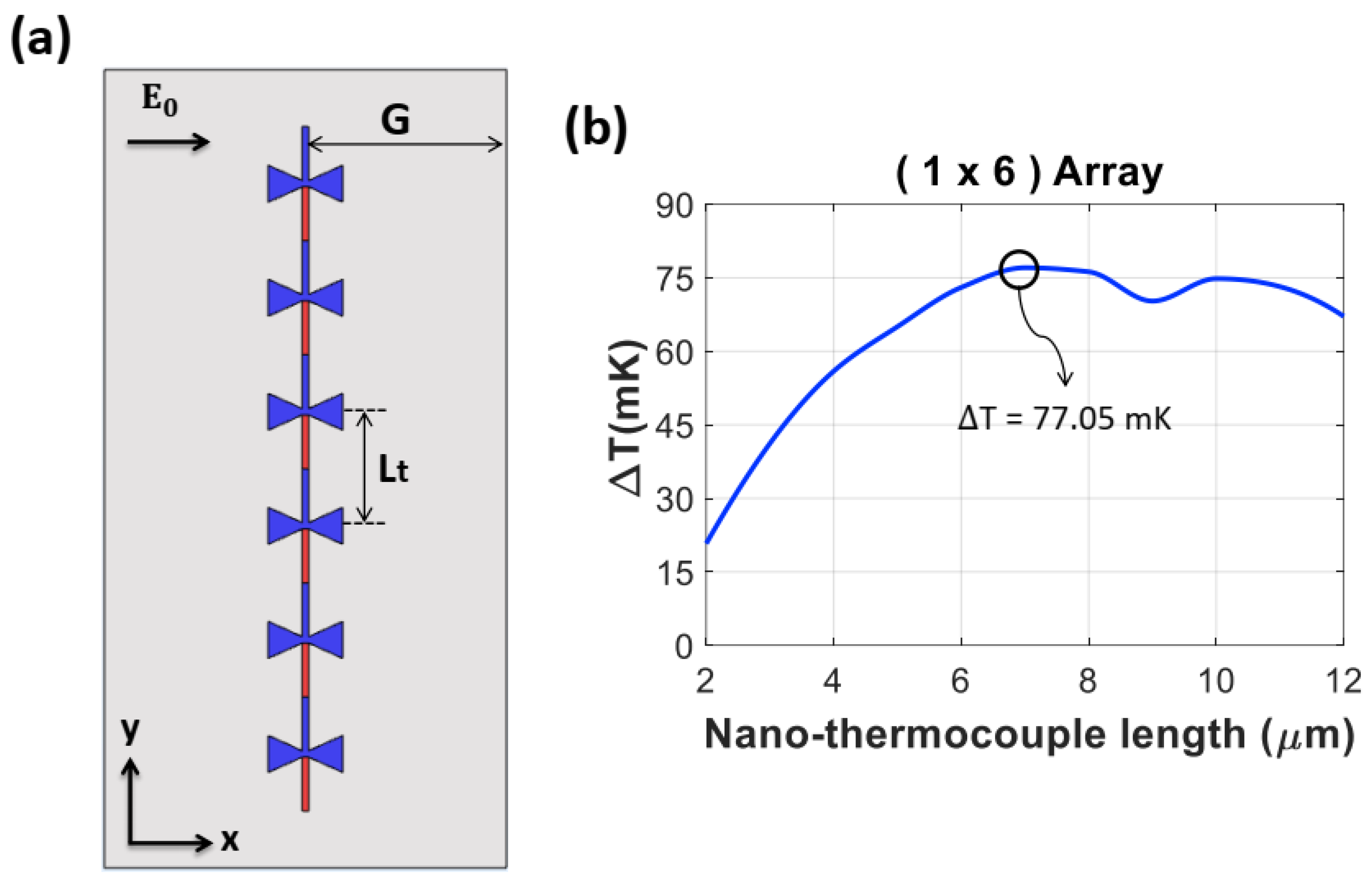
3.2.1. Optimization of Nano-Thermocouple Length Lt

We first designed a finite array of 1 × 6 antennas connected in series along the y-axis (Figure 5a) and tuned the nano-thermocouple length (Lt), the distance between the centers of adjacent antennas along the y-axis, to achieve the maximum ∆T at a resonant frequency of 28.3 THz. We maintained a distance from the antenna center to the substrate boundary (G) as 17.5 µm, half of the S (35 µm) used in the single antenna geometry. Figure 5b shows the average ∆T at a resonant frequency of 28.3 THz as a function of Lt, indicating a maximum ∆T of 77.05 mK at an Lt of 7 µm.
To gain a physical understanding of the dependence of Lt on ∆T, Figure 6 shows the electric field and temperature distributions on the xy plane in the middle of the antennas in the 1 × 6 antenna array at 28.3 THz for two cases: Lt = 7 µm and 5 µm. In both cases, the antennas in the array were constructively coupled to the standing wave at the center of the substrate, as shown in Figure 6a,c. Figure 6b,d confirm that the temperatures were elevated at all the antenna elements (hot junctions) compared with the ends of the nano-thermocouples (cold junctions). Although coupling occurred uniformly in both the hot and cold junctions, the optimal distance (Lt = 7 µm) between the antennas effectively suppressed the field at the ends of the thermocouple, resulting in uniformly lower temperatures at the cold junctions compared with those at the hot junctions, as shown in Figure 6b (inset). Consequently, the highest average ∆T was generated across all antennas when the Lt was 7 µm. Conversely, when the Lt was 5 µm, Figure 6d (inset) demonstrates that the temperature at the cold junctions was not sufficiently suppressed, resulting in a lower ∆T. This investigation revealed that the length of the thermocouple (Lt) connected to the nanoantenna must be optimized for suppressing the field strength at the cold junctions, even though all the antennas were constructively coupled to the standing wave generated by the SiO2 cavity.

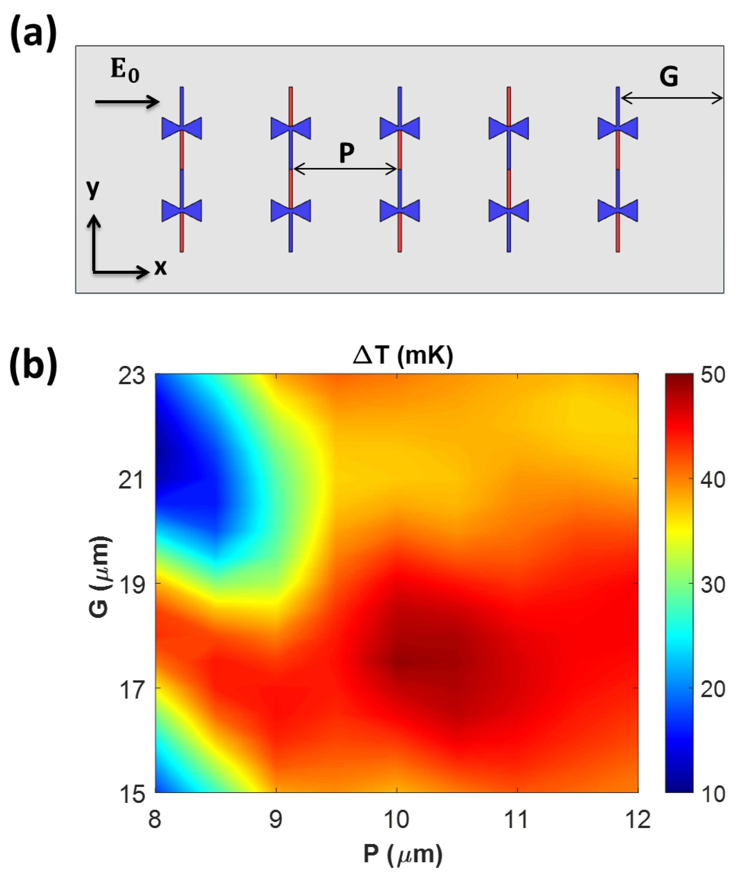
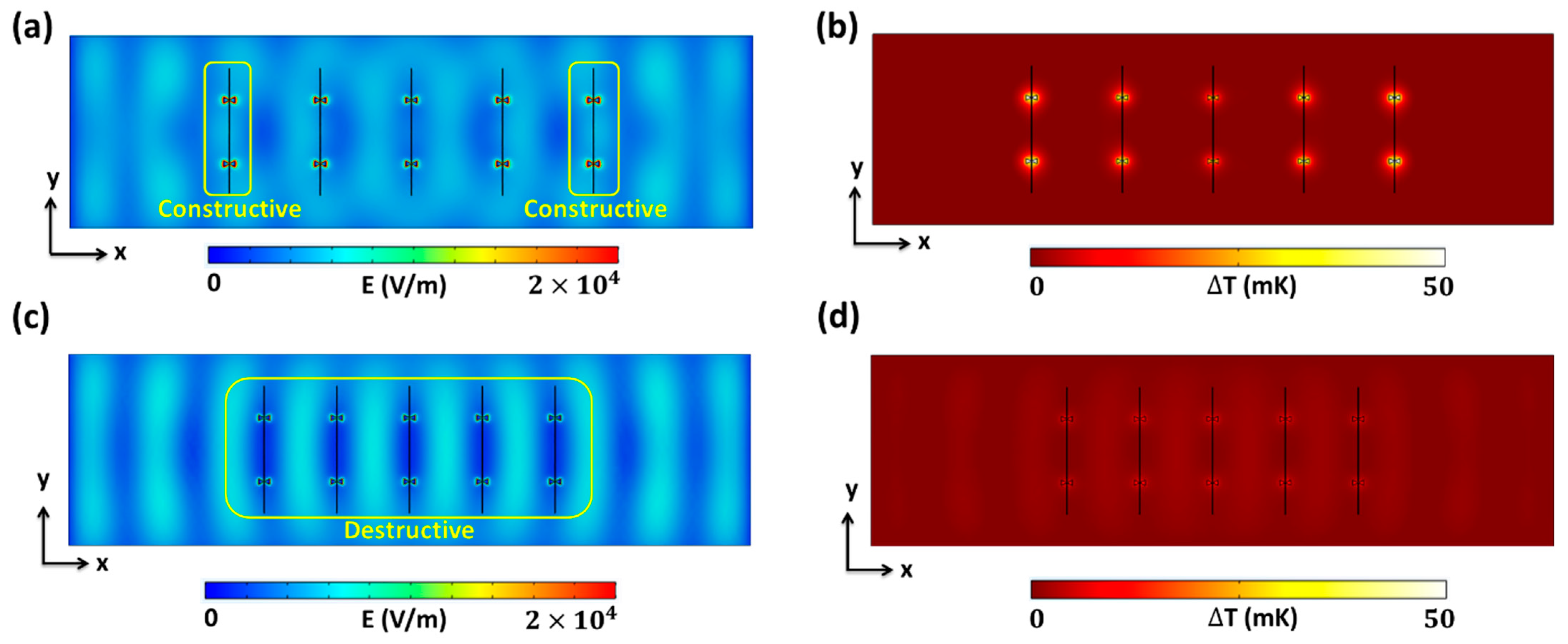
3.2.2. Optimization of Antenna Pitch (P) and Boundary Distance (G)

In addition to optimizing the Lt along the y-axis, we optimized the array geometry along the x-axis, including the antenna pitch (P) and the distance between the antenna near the boundary and substrate boundary (G) to achieve the maximum average T at 28.3 THz. In the optimization process, the P and G were simultaneously varied in a finite 5 × 2 array with a condition (G ≥ 15 µm), providing a sufficiently large area for five 1 × 2 arrays to be mounted stably, as shown in Figure 7a. All antennas were directed to the x-axis, parallel to the polarization of the incident wave, and the antennas in 1 × 2 arrays were arranged with Lt = 7 µm along the y-axis. Five pairs of 1 × 2 arrays were then arranged along the x-axis with different P and G values varying by 0.5 µm. Figure 7b presents the average ∆T distribution of the finite 5 × 2 array as a function of P and G at 28.3 THz. Specifically, P = 10 µm and G = 17.5 µm provided the maximum ∆T of 49.30 mK, while the minimum ∆T of 10.95 mK was observed at P = 8 µm and G = 21.5 µm. Using the relationship (S = 4P + 2G) between the substrate size along the x-axis (S), P, and G, both cases maintained the same S of 75 µm, which supported the TM90 mode in the substrate according to [28].
To investigate the coupling behavior between the antenna’s electric fields and standing waves from the substrate in two extreme cases, we analyzed the electric field and temperature distributions on the xy plane, as shown in Figure 8. Figure 8a,c reveal that the constructively and destructively coupled positions of the standing waves in the substrates were maintained in both cases, with only magnitude variations. The variation in field strength in the antennas was due to changes in the array positions along the x-axis. Specifically, Figure 8a, which corresponds to the maximum ∆T with P = 10 µm and G = 17.5 µm, shows that five 1 × 2 arrays were positioned along the x-axis to maximize the averaged field strength in the antennas. Due to the destructively coupled standing wave at the substrate center from the TM90 mode, the optimum P and G values located two arrays at constructively coupled positions near the boundaries, while one array at the center was located in a destructively coupled position. Conversely, in the minimum ∆T case with P = 8 µm and G = 21.5 µm, all the arrays were positioned at destructively coupled positions of the standing wave in the substrate. This coupling variation along the x-axis was translated into distinct ∆T differences between the two cases, as shown in Figure 8b,d. The higher coupling from the P = 10 µm and G = 17.5 µm case resulted in a highly elevated ∆T in all the antenna elements, as shown in Figure 8b. In addition, the non-uniform ∆T distribution in the five 1 × 2 arrays was evident, with the lowest ∆T occurring at the center of the arrays, approximately 24% lower compared with the average ∆T. Consequently, the maximum ∆T of 49.30 mK from the 5 × 2 array was lower than 77.05 mK from the 1 × 6 array, which had uniform coupling along the x-axis. For the lowest average ∆T case with P = 8 µm and G = 21.5 µm, Figure 8d shows weak ∆T distribution at the hot junctions due to destructively coupled positions in all antennas of the array. The simulation results confirmed that the optimum P and G in a finite substrate size (S) can enhance the Voc in the thermoelectric nanoantenna array structure by utilizing the coupling between the antenna’s electric field and the standing wave in the substrate.

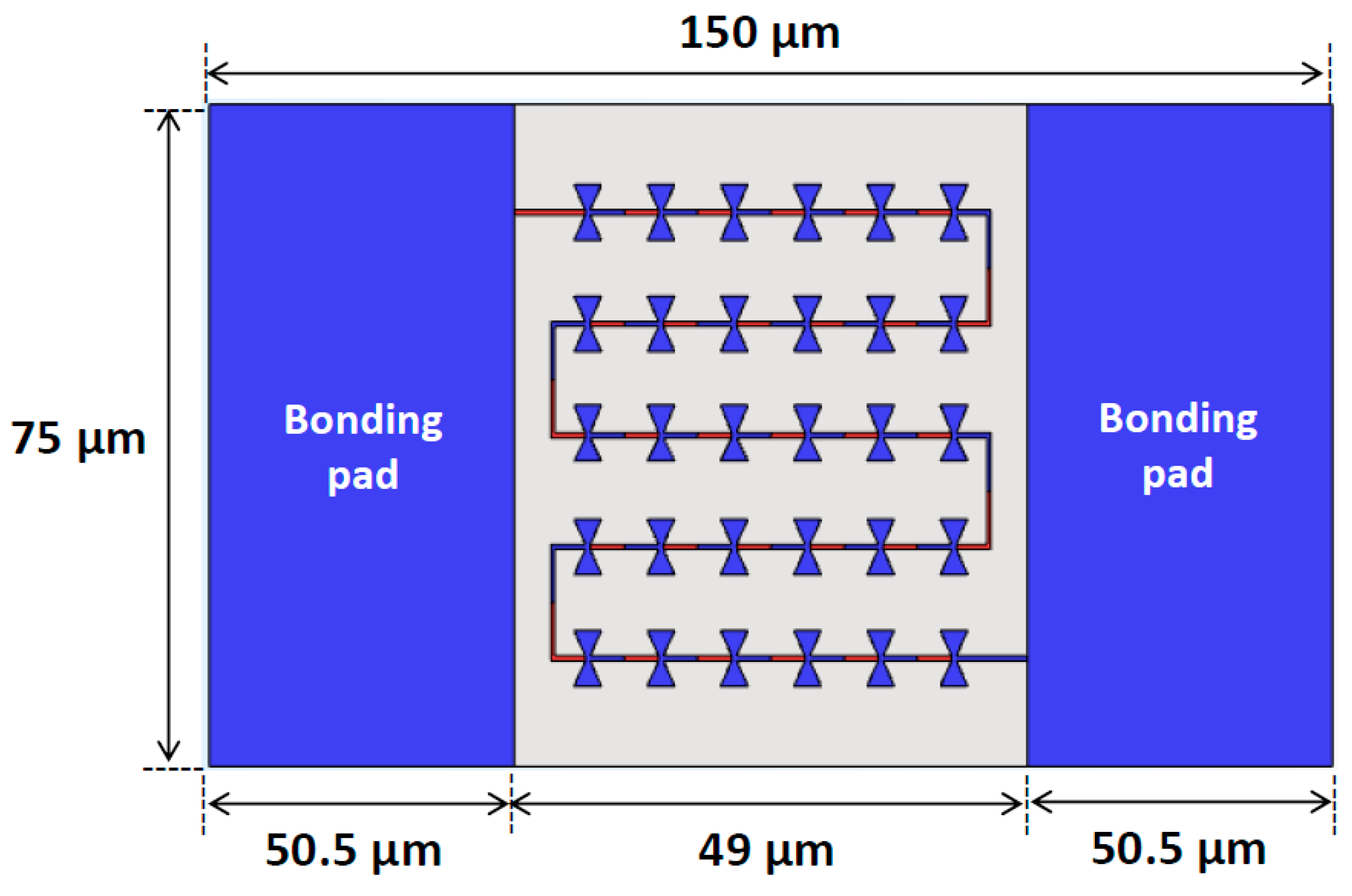
3.2.3. Finite 5 × 6 Thermoelectric Nanoantenna Array

Using the optimal values for the nano-thermocouple length (Lt) of 7 µm, antenna pitch (P) of 10 µm, and distance between the antenna and substrate boundary (G) of 17.5 µm, we designed a 5 × 6 finite array structure connected in series using 70 nm wide transmission lines (Figure 9a). The simulation results showed that the finite 5 × 6 arrays had an average ∆T of 48.37 mK. Using Voc = ΔS × ΔT, the Voc of the proposed structure was found to be 39.18 µV, which corresponded to an average Voc per antenna in the array of ~1.31 µV. This value outperformed a Voc of 1 µV from the suspended antenna over a cavity given the same input power of 1.42 W/cm2 [23].
To understand the heat distribution in the antennas and nano-thermocouple, the temperature distribution on the xy plane in the middle of the antennas is presented in Figure 9b. Figure 9b shows elevated ∆T values of approximately 50 mK near all the antenna elements with expected variations where antennas near the boundary maintained higher ∆T distributions compared to those near the center. This phenomenon occurred because the standing wave pattern in the substrate for the 5 × 6 array was the same as that of the finite 5 × 2 array. The difference in ∆T distribution between the two arrays is quantified by the δ d of the average ∆T. The value of the δ d from the finite 5 × 6 array was 11.08 mK, which was lower than 12.19 mK from the finite 5 × 2 array. This indicated that the finite 5 × 6 array maintained more uniformly distributed temperatures, attributable to additional heat flow through transmission lines connected to both ends of the series-connected array.
Overall, the proposed optimization methods achieved a ∆T of 48.37 mK with an average Voc of 1.31 µV per antenna. To ensure that the proposed devices generated the expected Voc in real measurements, bonding pads composed of Ti were added to the proposed finite thermoelectric nanoantenna array, as presented in Figure 10. With the addition of 75 µm × 50.5 µm bonding pads, the overall device size became 75 µm × 150 µm. The simulation results of the 5 × 6 array with bonding pads showed that the average ∆T generated from all the antennas in the array was 49.60 mK, corresponding to a total Voc of 40.18 µV and a Voc per antenna of 1.34 µV. The bonding pads did not perturb the ∆T of the antenna array due to their electrically large size compared with the antenna resonant wavelength. Lastly, if a device area of ~75 × 50 µm2 were scaled up to 1 cm2 with a massive array, then a high Voc of 1.07 V could be achieved.

3.3. Device’s Voltage Responsivity (βv) and Performance Comparison

Based on the maximum Voc generated by the finite 5 × 6 arrays of the thermoelectric nanoantenna, we further evaluated the device’s voltage responsivity (βv), defined as the ratio between the generated Voc and the incident power (Pin) for a fair comparison to other devices. The Pin of our device was 5.22 × 10⁻⁵ W, calculated by multiplying the effective area (Aeff) of 49 × 50 µm2 and the laser power density (Pd) of 1.42 W/cm2. Here, the physical substrate size where the arrays were laid out was used as the effective area. Finally, the ratio between the Voc of 40.18 µV and the Pin provided a βv of 0.77 V/W.
A performance comparison of the proposed work with other thermoelectric nanoantenna array structures is provided in Table 1. Our structure exhibited a similar or higher βv compared to thermoelectric antenna arrays using novel metals such as Ni or Pd [22,23,40]. In [23], a suspended nanoantenna array device over an air-filled cavity exhibited a βv of 0.64 V/W, which is lower than 0.77 V/W of our device. The high βv of the proposed array device was attributed to a temperature-boosting effect from the standing wave excited in the optimized open-ended and grounded substrate, along with the bowtie antenna topology, which had a higher effective aperture compared to the counterpart dipole antennas [22,23,40]. Recent numerical studies showed that metal nanoantennas coupled with telluride-based high-ZT materials such as Bi2Te3 and Sb2Te3 achieved a much higher βv of ~50 V/W [41,42]. This difference can be mostly attributed to a higher Seebeck coefficient compared to that of novel metals. Therefore, if materials with a higher Seebeck coefficient are applied in the proposed nanoantenna array structure, the βv could be further improved.

4. Conclusions

We introduced a high-output voltage IR-harvesting device based on a bowtie nanoantenna array combined with a bimetal nano-thermocouple mounted on a finite SiO2 substrate. First, the optimal thermoelectric antenna element for achieving the maximum Voc was found. The optimum structure was a single metal nanoantenna with low thermal conductivity among two metals used in the bimetal thermocouple, and the antenna was perpendicularly connected to the thermocouple. Subsequently, we designed a finite array structure by optimizing the nano-thermocouple length (Lt), antenna pitch (P), and distance between the antenna and the substrate boundary (G). The optimal values of Lt, P, and G were 7 µm, 10 µm, and 17.5 µm, respectively, in a finite 5 × 6 array with 30 thermoelectric antennas connected in series. In numerical simulations, the final thermoelectric nanoantenna array structure exhibited a ∆T of 49.60 mK between the hot and cold junctions, equal to a Voc of 40.18 µV. This indicated that the average Voc associated with one antenna was ~1.34 µV with a β v of 0.77 V/W, surpassing the previously reported values of ~1 µV and 0.64 V/W for a thermoelectric nanoantenna arrays using the same input power density of 1.42 W/cm2 [23]. In addition, the proposed design is expected to demonstrate better stability in real fabrication because the antenna and the nano-thermocouple are directly placed on the substrate, rather than being suspended over the air-filled cavity [23]. Consequently, the proposed optimum thermoelectric nanoantenna array design utilizing the finite and grounded SiO2 substrate offers a viable solution for enhancing the output voltage of IR harvesting devices and sensors.

Author Contributions

M.K.A. conducted the numerical simulations and designed the structures. Y.Y. conducted the numerical simulations. S.C. conceived the concept and supervised the research. All authors analyzed the results and drafted the manuscript. All authors have read and agreed to the published version of the manuscript.

Funding

This research was supported by Kyungpook National University Research Fund (202237620000), 2022.

Data Availability Statement

Data are contained within the article.

Conflicts of Interest

The authors declare no conflicts of interest.

References

  1. Hudson, R.D. Infrared System Engineering; Wiley-Interscience: New York, NY, USA, 1969; Volume 1. [Google Scholar]
  2. Tritt, T.M.; Böttner, H.; Chen, L. Thermoelectrics: Direct Solar Thermal Energy Conversion. MRS Bull. 2008, 33, 366–368. [Google Scholar] [CrossRef]
  3. Hu, R.; Cola, B.A.; Haram, N.; Barisci, J.N.; Lee, S.; Stoughton, S.; Wallace, G.; Too, C.; Thomas, M.; Gestos, A. Harvesting Waste Thermal Energy Using a Carbon-Nanotube-Based Thermo-Electrochemical Cell. Nano Lett. 2010, 10, 838–846. [Google Scholar] [CrossRef]
  4. Jayaswal, G.; Belkadi, A.; Meredov, A.; Pelz, B.; Moddel, G.; Shamim, A. Optical Rectification through an Al2O3 Based MIM Passive Rectenna at 28.3 THz. Mater. Today Energy 2018, 7, 1–9. [Google Scholar] [CrossRef]
  5. Davids, P.S.; Kirsch, J.; Starbuck, A.; Jarecki, R.; Shank, J.; Peters, D. Electrical Power Generation from Moderate-Temperature Radiative Thermal Sources. Science 2020, 367, 1341–1345. [Google Scholar] [CrossRef] [PubMed]
  6. Codreanu, I.; Gonzalez, F.J.; Boreman, G.D. Detection Mechanisms in Microstrip Dipole Antenna-Coupled Infrared Detectors. Infrared Phys. Technol. 2003, 44, 155–163. [Google Scholar] [CrossRef]
  7. Bean, J.A.; Tiwari, B.; Bernstein, G.H.; Fay, P.; Porod, W. Thermal Infrared Detection Using Dipole Antenna-Coupled Metal-Oxide-Metal Diodes. J. Vac. Sci. Technol. B Microelectron. Nanometer Struct. Process. Meas. Phenom. 2009, 27, 11–14. [Google Scholar] [CrossRef]
  8. Vandenbosch, G.A.; Ma, Z. Upper Bounds for the Solar Energy Harvesting Efficiency of Nano-Antennas. Nano Energy 2012, 1, 494–502. [Google Scholar] [CrossRef]
  9. Coppens, Z.J.; Li, W.; Walker, D.G.; Valentine, J.G. Probing and Controlling Photothermal Heat Generation in Plasmonic Nanostructures. Nano Lett. 2013, 13, 1023–1028. [Google Scholar] [CrossRef]
  10. Grosse, K.L.; Bae, M.-H.; Lian, F.; Pop, E.; King, W.P. Nanoscale Joule Heating, Peltier Cooling and Current Crowding at Graphene–Metal Contacts. Nat. Nanotechnol. 2011, 6, 287–290. [Google Scholar] [CrossRef]
  11. Li, D.; Sharma, A.A.; Gala, D.K.; Shukla, N.; Paik, H.; Datta, S.; Schlom, D.G.; Bain, J.A.; Skowronski, M. Joule Heating-Induced Metal–Insulator Transition in Epitaxial VO2/TiO2 Devices. ACS Appl. Mater. Interfaces 2016, 8, 12908–12914. [Google Scholar] [CrossRef]
  12. Perrin, N.; Budd, H. Photon Generation by Joule Heating in Metal Films. Phys. Rev. Lett. 1972, 28, 1701. [Google Scholar] [CrossRef]
  13. Datta, S. Quantum Transport: Atom to Transistor; Cambridge University Press: Cambridge, UK, 2005. [Google Scholar]
  14. Rowe, D.M. CRC Handbook of Thermoelectrics; CRC Press: Boca Raton, FL, USA, 2018. [Google Scholar]
  15. Van Herwaarden, A.W.; Sarro, P.M. Thermal Sensors Based on the Seebeck Effect. Sens. Actuators 1986, 10, 321–346. [Google Scholar] [CrossRef]
  16. Zhou, W.; Yamamoto, K.; Miura, A.; Iguchi, R.; Miura, Y.; Uchida, K.; Sakuraba, Y. Seebeck-Driven Transverse Thermoelectric Generation. Nat. Mater. 2021, 20, 463–467. [Google Scholar] [CrossRef]
  17. Witting, I.T.; Chasapis, T.C.; Ricci, F.; Peters, M.; Heinz, N.A.; Hautier, G.; Snyder, G.J. The Thermoelectric Properties of Bismuth Telluride. Adv Elect Mater. 2019, 5, 1800904. [Google Scholar] [CrossRef]
  18. Dughaish, Z.H. Lead Telluride as a Thermoelectric Material for Thermoelectric Power Generation. Phys. B Condens. Matter 2002, 322, 205–223. [Google Scholar] [CrossRef]
  19. Blackburn, J.L.; Ferguson, A.J.; Cho, C.; Grunlan, J.C. Carbon-Nanotube-Based Thermoelectric Materials and Devices. Adv. Mater. 2018, 30, 1704386. [Google Scholar] [CrossRef]
  20. Szakmany, G.P.; Orlov, A.O.; Bernstein, G.H.; Porod, W. Polarization-Dependent Response of Single-and Bi-Metal Antenna-Coupled Thermopiles for Infrared Detection. IEEE Trans. Terahertz Sci. Technol. 2015, 5, 884–891. [Google Scholar] [CrossRef]
  21. Szakmany, G.P.; Orlov, A.O.; Bernstein, G.H.; Porod, W. Fabrication of Suspended Antenna-Coupled Nanothermocouples. J. Vac. Sci. Technol. B Nanotechnol. Microelectron. Mater. Process. Meas. Phenom. 2019, 37, 052201. [Google Scholar] [CrossRef]
  22. Szakmany, G.P.; Orlov, A.O.; Bernstein, G.H.; Porod, W. Nanoantenna Arrays for Infrared Detection with Single-Metal Nanothermocouples. Infrared Phys. Technol. 2017, 82, 44–49. [Google Scholar] [CrossRef]
  23. Szakmany, G.P.; Bernstein, G.H.; Orlov, A.O.; Porod, W. Suspended Antenna-Coupled Nanothermocouple Array for Long-Wave Infrared Detection. In Proceedings of the ESSDERC 2019—49th European Solid-State Device Research Conference (ESSDERC), Cracow, Poland, 23–26 September 2019; pp. 258–261. [Google Scholar]
  24. González, F.J.; Dhakal, N.; Boykin, T.; Méndez-Lozoya, J.; Peale, R.E. Infrared Pixel Based on Seebeck Nanoantennas. MRS Adv. 2020, 5, 1837–1842. [Google Scholar] [CrossRef]
  25. Briones, E.; Kuri, C.; Cortes-Mestizo, I.; Briones, J.; Vilchis, H. Numerical Conversion Efficiency of Thermally Isolated Seebeck Nanoantennas. AIP Adv. 2016, 6, 115018. [Google Scholar] [CrossRef]
  26. Szakmany, G.P.; Orlov, A.O.; Bernstein, G.H.; Porod, W. Cavity-Backed Antenna-Coupled Nanothermocouples. Sci. Rep. 2019, 9, 9606. [Google Scholar] [CrossRef]
  27. Finnan, C.P.; Kinzel, E.C.; Szakmany, G.P.; Orlov, A.O.; Aquino, H.R.O.; Porod, W.; Bernstein, G.H. Performance of Ultrafast, Nanoantenna-Based, Long-Wave Infrared Detectors in Vacuum. IEEE Sens. J. 2024, 24, 6092–6102. [Google Scholar] [CrossRef]
  28. Anam, M.K.; Choi, S. Infrared Thermoelectric Nanoantenna with Maximum Output Voltage Using Grounded and Open-Ended SiO2. Adv. Opt. Mater. 2022, 11, 2201767. [Google Scholar] [CrossRef]
  29. Ordal, M.A.; Bell, R.J.; Alexander, R.W.; Long, L.L.; Querry, M.R. Optical Properties of Au, Ni, and Pb at Submillimeter Wavelengths. Appl. Opt. 1987, 26, 744–752. [Google Scholar] [CrossRef]
  30. Ordal, M.A.; Bell, R.J.; Alexander, R.W.; Newquist, L.A.; Querry, M.R. Optical Properties of Al, Fe, Ti, Ta, W, and Mo at Submillimeter Wavelengths. Appl. Opt. 1988, 27, 1203–1209. [Google Scholar] [CrossRef]
  31. Kischkat, J.; Peters, S.; Gruska, B.; Semtsiv, M.; Chashnikova, M.; Klinkmüller, M.; Fedosenko, O.; Machulik, S.; Aleksandrova, A.; Monastyrskyi, G. Mid-Infrared Optical Properties of Thin Films of Aluminum Oxide, Titanium Dioxide, Silicon Dioxide, Aluminum Nitride, and Silicon Nitride. Appl. Opt. 2012, 51, 6789–6798. [Google Scholar] [CrossRef]
  32. Lide, D.R. CRC Handbook of Chemistry and Physics; CRC Press: Boca Raton, FL, USA, 2004; Volume 85. [Google Scholar]
  33. Kresse, G.; Furthmüller, J. Efficient Iterative Schemes for Ab Initio Total-Energy Calculations Using a Plane-Wave Basis Set. Phys. Rev. B 1996, 54, 11169–11186. [Google Scholar] [CrossRef]
  34. Mora-Ventura, B.; Sánchez, J.E.; González, G.; González, F.J. Thermal Impedance Analysis of Nano-Dipole Linear Arrays for Energy Harvesting Applications. Infrared Phys. Technol. 2020, 107, 103332. [Google Scholar] [CrossRef]
  35. Mattsson, C.G.; Bertilsson, K.; Thungström, G.; Nilsson, H.-E.; Martin, H. Thermal Simulation and Design Optimization of a Thermopile Infrared Detector with an SU-8 Membrane. J. Micromech. Microeng. 2009, 19, 055016. [Google Scholar] [CrossRef]
  36. Rowe, D.M. Thermoelectrics Handbook: Macro to Nano; CRC Press: Boca Raton, FL, USA, 2018. [Google Scholar]
  37. Krenz, P.M.; Tiwari, B.; Szakmany, G.P.; Orlov, A.O.; González, F.J.; Boreman, G.D.; Porod, W. Response Increase of IR Antenna-Coupled Thermocouple Using Impedance Matching. IEEE J. Quantum Electron. 2012, 48, 659–664. [Google Scholar] [CrossRef]
  38. Szakmany, G.P.; Krenz, P.M.; Orlov, A.O.; Bernstein, G.H.; Porod, W. Antenna-Coupled Nanowire Thermocouples for Infrared Detection. IEEE Trans. Nanotechnol. 2012, 12, 163–167. [Google Scholar] [CrossRef]
  39. Szakmany, G.P.; Krenz, P.M.; Schneider, L.C.; Orlov, A.O.; Bernstein, G.H.; Porod, W. Nanowire Thermocouple Characterization Platform. IEEE Trans. Nanotechnol. 2013, 12, 309–313. [Google Scholar] [CrossRef]
  40. Szakmany, G.P.; Bernstein, G.H.; Kinzel, E.C.; Orlov, A.O.; Porod, W. Nanoantenna-Based Ultrafast Thermoelectric Long-Wave Infrared Detectors. Sci. Rep. 2020, 10, 13429. [Google Scholar] [CrossRef]
  41. González, F.J.; Peale, R.E. Design and Optimization of an Infrared Pixel Based on Seebeck Nanoantennas. In Proceedings of the Infrared Remote Sensing and Instrumentation XXIX; SPIE: Bellingham, WA, USA, 2021; Volume 11830, pp. 42–46. [Google Scholar]
  42. Moreno, J.R.; González, F.J. Infrared Pixel Based on Seebeck Nanoantennas for Plane Array Detectors. In Proceedings of the Infrared Remote Sensing and Instrumentation XXX; SPIE: Bellingham, WA, USA, 2022; Volume 12233, pp. 135–140. [Google Scholar]
Figure 1. Schematic of the thermoelectric nanoantenna simulation, where an incident electric field (E0) aligned with the antenna axis and propagated in the negative z-direction. The simulation boundary was defined as a perfectly matched layer (PML).
Nanomaterials 14 01159 g001
Figure 2. Schematics of the single antennas with different geometries. (a) Bimetal antenna connected in parallel with a nano-thermocouple (geometry I), (b) bimetal antenna connected perpendicularly with a nano-thermocouple (geometry II), and (c) single metal antenna connected perpendicularly with a nano-thermocouple (geometry III). (d) Schematic of a single thermoelectric nanoantenna (geometry III) mounted on a SiO2-grounded substrate.
Nanomaterials 14 01159 g002
Figure 3. Electric field and temperature distribution on the xy plane in the middle of the antenna at 28.3 THz for (a,d) geometry I, (b,e) geometry II, and (c,f) geometry III.
Nanomaterials 14 01159 g003
Figure 4. (a) ΔT and (b) Voc for three single thermoelectric nanoantenna geometries as a function of frequency.
Nanomaterials 14 01159 g004
Figure 5. (a) Schematic of the 1 × 6 array of thermoelectric nanoantennas on the xy plane. The nano-thermocouple length (Lt) is the distance between two antennas along the vertical axis (y-axis). (b) Average ∆T at a resonant frequency of 28.3 THz as a function of Lt.
Nanomaterials 14 01159 g005
Figure 6. Electric field and temperature distributions on the xy plane in the middle of the antennas in the 1 × 6 antenna array at 28.3 THz. Figures (a,b) and (c,d) correspond to Lt = 7 µm and Lt = 5 µm, respectively.
Nanomaterials 14 01159 g006
Figure 7. (a) Schematic of a 5 × 2 array of thermoelectric nanoantennas, indicating the antenna pitch (P), the distance between the antenna center in the horizontal axis (x-axis), and the distance between the antenna near the boundary and substrate boundary (G). (b) Contour plot of ΔT with different P and G values.
Nanomaterials 14 01159 g007
Figure 8. Electric field and temperature distribution of the 5 × 2 antenna array on the xy plane in the middle of the antennas at 28.3 THz. (a,b) P = 10 µm, G = 17.5 µm; and (c,d) P = 8 µm, G = 21.5 µm.
Nanomaterials 14 01159 g008
Figure 9. (a) Schematic of finite 5 × 6 arrays, consisting of 30 antennas connected in series. (b) Temperature distribution on the xy plane in the middle of the antenna at 28.3 THz.
Nanomaterials 14 01159 g009
Figure 10. Schematic of the proposed thermoelectric antenna array with 5 × 6 antenna elements with the bonding pads.
Nanomaterials 14 01159 g010
Table 1. Performance comparison of the voltage responsivity (βv) with other state-of-the-art thermoelectric nanoantenna arrays.
Ref.Antenna
Topology
(Material)
ThermocoupleSubstrate# of
Antennas
Power
Density
(W/cm2)
Aperture Size
(µm2)
Voc
(µV)
βv
(V/W)
[22]Dipole (Pd)PdGrounded SiO24401.427.04   ×   10 3 3.250.032
[23]Dipole (Pd)Ni-PdAir-filled cavity2001.422.2   ×   10 4 2000.64
[40]Dipole (Pd)Ni-PdAir-filled cavity521.426 0   ×   10 3 9.370.011
[41]Bowtie (Au)Bi2Te3-Sb2Te3Air-filled cavity160.11.1   ×   10 3 5550
[42]Dipole (Au)Bi2Te3-NiAir-filled cavity160.15.76   ×   10 3 3052.08 (40 THz)
This workBowtie (Ti)Ni-TiOpen-ended and grounded SiO2301.423.67   ×   10 3 40.180.77
All the Voc and βv values are maximal at 28.3 THz if the frequency is not specified.
Disclaimer/Publisher’s Note: The statements, opinions and data contained in all publications are solely those of the individual author(s) and contributor(s) and not of MDPI and/or the editor(s). MDPI and/or the editor(s) disclaim responsibility for any injury to people or property resulting from any ideas, methods, instructions or products referred to in the content.

