Article

Polarized Raman Study of First-Order Phonons in Self-Flux Grown Single-Crystalline WTe2

1
“G. Nadjakov” Institute of Solid State Physics, Bulgarian Academy of Sciences, 1784 Sofia, Bulgaria
2
Institute of Optical Materials and Technologies, Bulgarian Academy of Sciences, 1113 Sofia, Bulgaria
3
Institute of General and Inorganic Chemistry, Bulgarian Academy of Sciences, 1113 Sofia, Bulgaria
*
Author to whom correspondence should be addressed.
Nanomaterials 2024, 14(15), 1256; https://doi.org/10.3390/nano14151256 (registering DOI)
Submission received: 19 May 2024 / Revised: 18 July 2024 / Accepted: 21 July 2024 / Published: 27 July 2024
(This article belongs to the Section 2D and Carbon Nanomaterials)

Abstract

:
Bulk single crystals of WTe2 were grown by the self-flux method and characterized by X-ray diffraction, polarized micro-Raman spectroscopy, and optical microscopy. All methods revealed a high crystalline quality, thus demonstrating the advantages of the growth method used as a starting base for the synthesis of high-quality 2D materials. In each main scattering configuration, we recorded a series of Raman spectra in different sample orientations achieved by rotating the sample around the incident laser beam. In addition to the well-established case of excitation along the c crystal axis, we also applied laser excitation along the a and b axes. Thus, scattering configurations were also realized in the XZ and YZ polarization planes, for which no comparative literature data have yet been established. In these experiments, two new Raman-active phonons with B2 symmetry and frequencies of 89 cm−1 and 122 cm−1 were identified. The obtained experimental data enabled us to derive the magnitude ratios of all three tensor elements of the A1 modes and to find their phase differences.

1. Introduction

Tungsten ditelluride (WTe2), a member of the transition metal dichalcogenides (TMDs) family [1], due to its unique electronic and structural properties, exhibits a rich array of phenomena, including large and anisotropic magnetoresistance [2], unconventional superconductivity [3], and the potential for hosting exotic quantum states [4]. Its intriguing behaviour has sparked intense research interest, driven both by fundamental scientific curiosity and the promise of novel technological applications.
The layered crystal structure of WTe2, comprising stacked atomic layers held together by weak van der Waals forces [5], endows it with remarkable two-dimensional characteristics, reminiscent of other TMDs like graphene and molybdenum disulfide (MoS2) [6]. However, unlike its counterparts, WTe2 exhibits a unique combination of broken inversion symmetry and strong spin-orbit coupling leading to intriguing electronic band structures and topologically non-trivial properties [7].
One of the most striking features of WTe2 is its pronounced and unconventional magnetoresistance behaviour, characterized by a colossal and highly anisotropic response to external magnetic fields [8]. This phenomenon has gathered significant attention for its potential in spintronic and quantum computing applications, as well as for its fundamental implications on our understanding of electronic transport in low-dimensional systems.
Furthermore, recent experimental investigations have unveiled evidence of superconductivity in WTe2 under specific conditions [9], further adding to its allure as a platform for exploring novel quantum phenomena. The interplay between superconductivity, magnetism, and topology in WTe2 presents a fertile ground for studying emergent quantum states and exotic phase transitions.
Synthesizing atomically thin layers of WTe2 presents a formidable challenge due to the intrinsic properties of the material and the delicate balance required to achieve monolayer or few-layer flakes with high quality and uniformity [10]. This is especially true for 2D WTe2 achieved through the direct conversion of metal and metal-oxide films due to the low reactivity between tellurium and the transition metal tungsten [11]. Techniques such as chemical vapor deposition (CVD) and molecular beam epitaxy (MBE), while promising, often struggle to produce large-area, defect-free 2D samples, limiting their applicability in certain experimental studies and device applications.
In contrast, the synthesis of bulk crystals of WTe2 offers distinct advantages in terms of quality and reproducibility [12]. High-temperature methods such as chemical vapor transport (CVT) or flux-growth techniques enable the production of large, high-purity crystals with well-defined structural and electronic properties. While high-quality single crystals can be grown using the CVT [13] method, the self-flux [14] method consistently yields even higher-quality single crystals. In the CVT method, the transport agents can introduce impurities into the crystal. On the other hand, in the self-flux method, the low melting point and high boiling point of elemental Te provide a large temperature window to grow crystals from the melt. Additionally, the absence of a transport agent eliminates a source of impurities. Studies [14] have shown that the residual resistivity ratio (RRR) of flux-grown crystals reaches much higher values compared to those of CVT-grown crystals, implying fewer defects and impurities and leading to an order of magnitude higher magnetoresistance [15]. The self-flux crystal growth method has been successfully used for the synthesis of other TMDs, such as PdSe2 [16], WSe2, and MoSe2 [17,18]. The high-quality bulk crystals grown by this method serve as invaluable platforms for conducting precise measurements and exploring fundamental phenomena, providing insights that complement those obtained from 2D samples.
WTe2 has particularly attracted significant interest due to the extremely large magnetoresistance effect in the otherwise diamagnetic WTe2 single crystal—a phenomenon not matched in other TMDCs [2]. There is also a remarkably strong dependence of the resistivity on the thickness of WTe2 multilayer flakes [19]. Given these properties and the resulting application prospects, a detailed knowledge of the vibrational structure of WTe2 is of essential importance.
Several studies have been devoted to the Raman response of crystalline WTe2 [19,20,21,22,23,24,25,26]. Due to sample constraints, these studies used only back-scattering experiments from the XY surface with exciting laser beam perpendicular to the layers. Under these conditions, only vibrational modes of A1 and A2 symmetry could be detected. Here, we report the synthesis of sufficiently large free-standing WTe2 single crystals using the self-flux crystal growth method, followed by detailed Raman characterization in all essential polarization geometries without restriction to the XY surface. We detected two new Raman active modes of B2 symmetry and obtained some important characteristics of all three elements of the A1 Raman tensors.

2. Materials and Methods

WTe2 single crystals were obtained by a self-flux method using tellurium flux, taking advantage of the very slight solubility [14] of W and WTe2 in tellurium. The method is reproducible and yields consistently higher-quality single crystals than are typically obtained via halide-assisted vapor transport methods. In a typical recipe, 9.195 g of W and 230 g of purified Te (99.9999%) were sealed in an evacuated quartz tube. A small amount of quartz wool was added to the tube to act as a filter in order to separate the flux material from the crystals in a later step. The tube was then heated to 825 °C, held there for 24 h, and then cooled at a rate of 2–3 °C/h to 525 °C. At this temperature, the flux was separated from the crystals by inverting the tube. The WTe2 crystals were then put in another vacuum-sealed quartz tube and heated to 415 °C in a tube furnace, with WTe2 crystals on the hot end and the cold end held at 200 °C. This was done for 2 days in order to separate excess Te from the crystal surfaces via self-vapor-transport and to anneal the crystals. Under these conditions, several lengthy ribbon-like WTe2 crystals of mm size were obtained.
X-ray diffraction patterns were collected within the 2θ range from 10 to 80° with a constant step of 0.02° on a Bruker D8 Advance diffractometer (Billerica, MA, USA) with tube CuKα 40 KV, 40 mA. Goniometer radius 217.5 mm, scan type coupled TwoTheta/Theta, 10–80°, step 0.02, counting time 35 s/step, primary Soller slit 4°, divergent slit 0.3°, secondary Soller slit 4°, anti-scattered slit 0.5°, LynxEye detector (Billerica, MA, USA) and detector slit 11.93 mm. Phase identification was performed with the Diffracplus EVA using the ICDD-PDF2 Database (Newtown Square, PA, USA).
The Raman spectra were measured in backscattering geometry using a HORIBA Jobin Yvon Labram HR-visible spectrometer (HORIBA Scientific, Kyoto, Japan) equipped with a Peltier-cooled CCD detector. The 632.8 nm line of a He-Ne laser was used for excitation. The laser beam was focused on a spot of about 1–2 µm in diameter on the sample surface using microscope optics. A diffraction grating of 1800 lines·mm−1 was used for dispersing the Raman signal, assuring a spectral resolution better than 1 cm−1. The laser power was attenuated below 500 µW to avoid sample overheating. Si standard was used to calibrate the frequency, and the line intensities were determined by fitting them to Voigt profiles.

3. Results

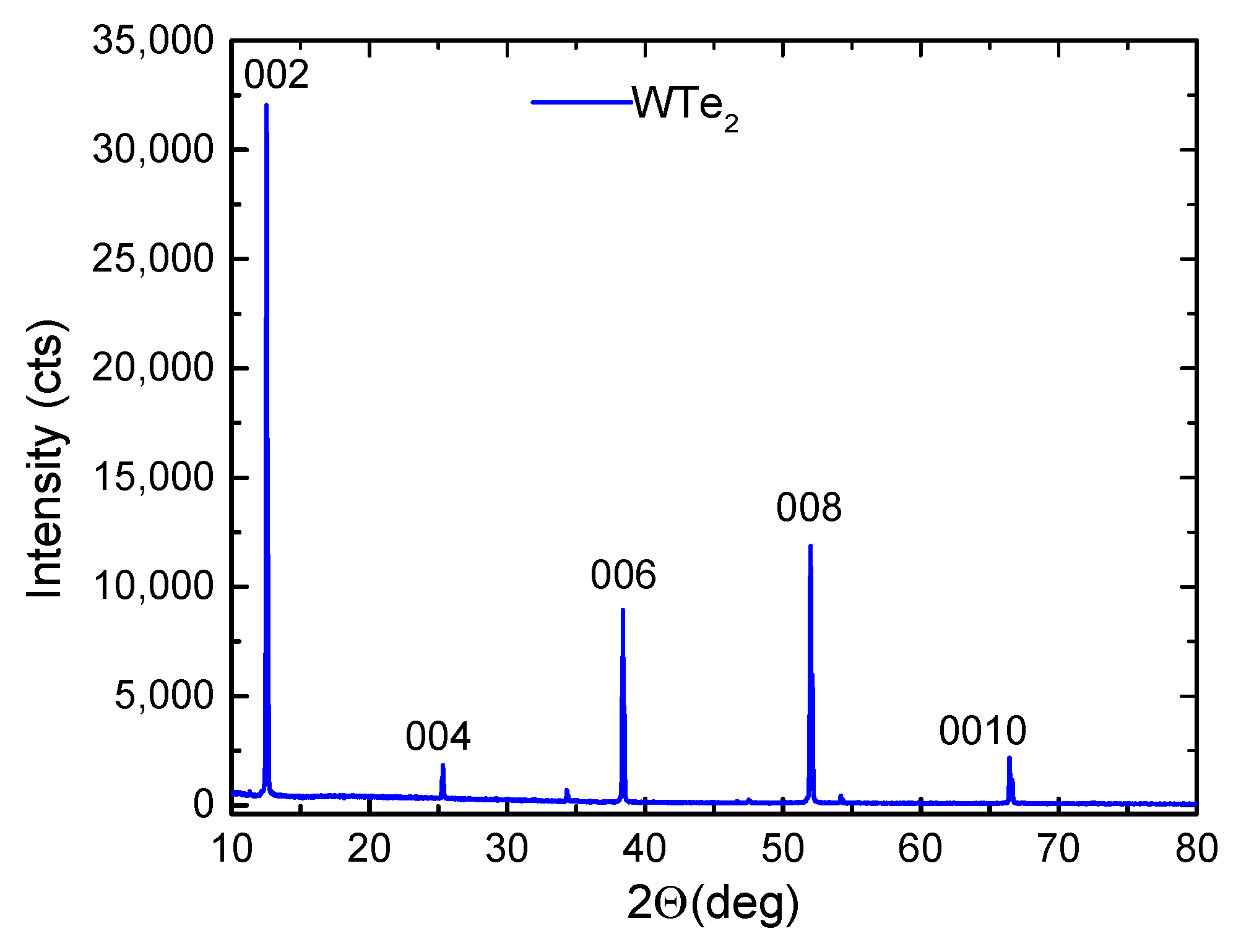
3.1. X-ray Diffraction Analysis
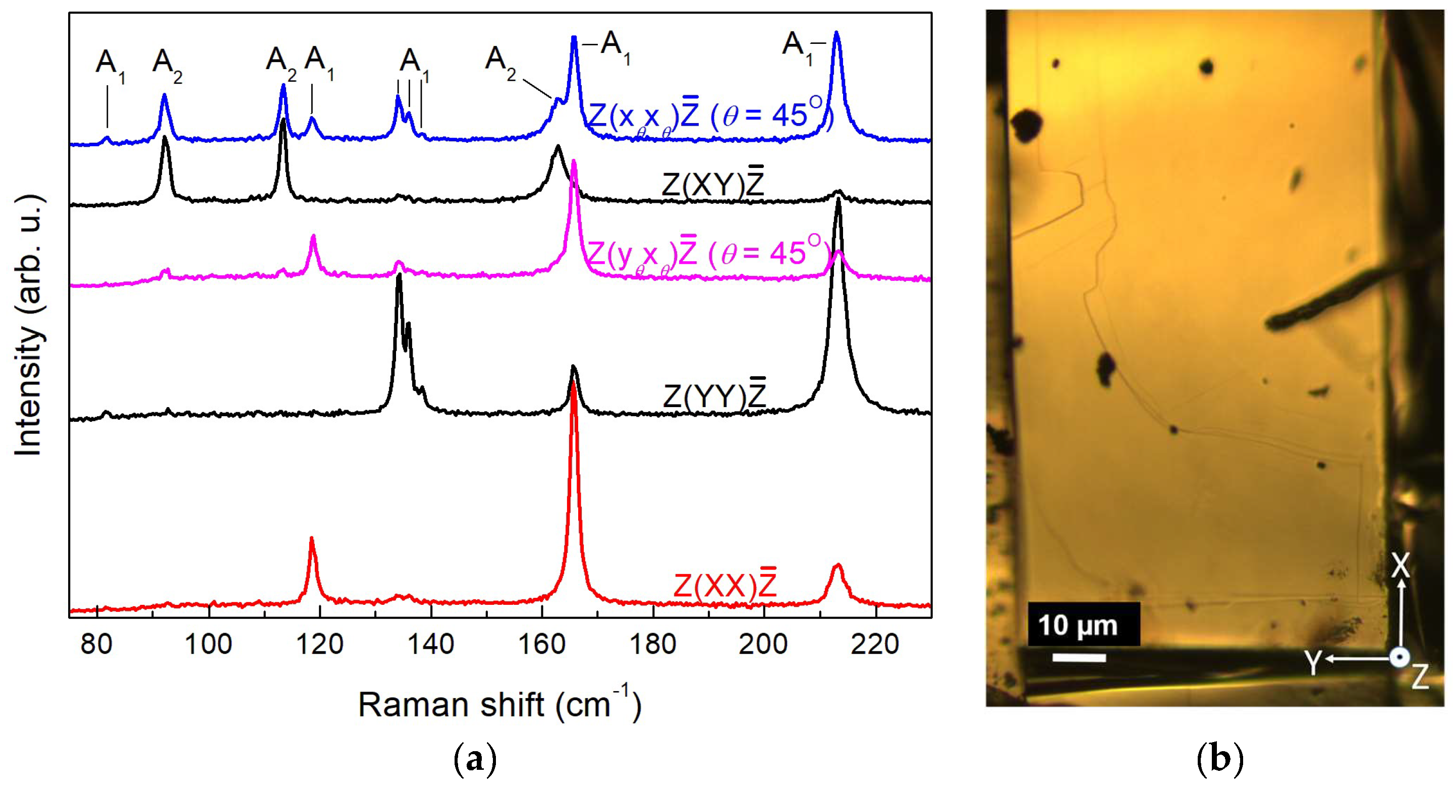
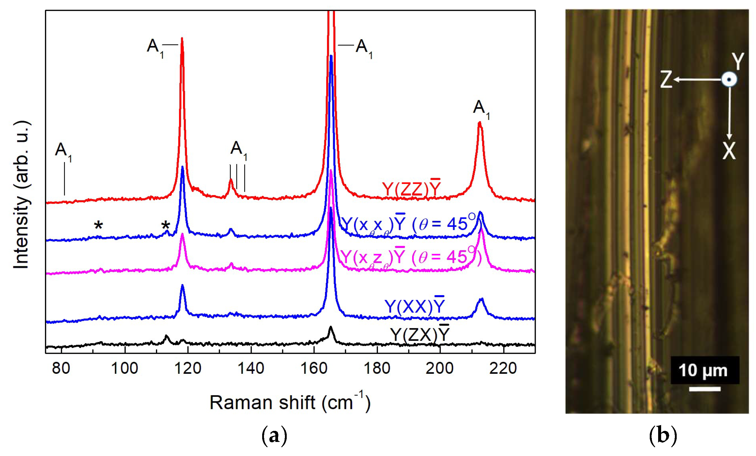
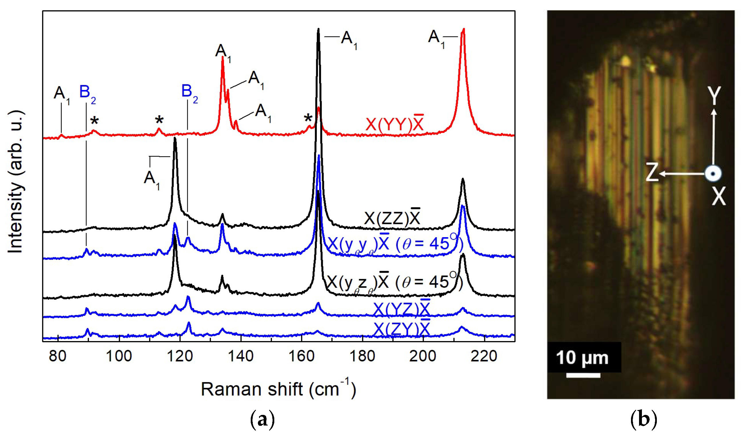
Tungsten ditelluride (WTe2) exhibits a unique crystal structure with an orthorhombic lattice belonging to the Pmn21 space group [27,28,29]. The material possesses a large interlayer spacing and a semi-metallic electronic structure. In its crystalline form, WTe2 comprises two-dimensional layers oriented in the (0, 0, 1) direction [2]. Each layer consists of distorted edge-sharing WTe6 pentagonal pyramids, with W4+ atoms bonded to six Te2− atoms, as depicted in Figure 1 [13].
The crystal structure of WTe2 contrasts with other transition metal dichalcogenides (TMDs) like MoS2, which typically have a hexagonal lattice. In WTe2, the triple-layer Te-W-Te atomic planes crystallize in an orthorhombic, distorted-1T structure with C2v symmetry [14]. Although the chalcogenides around the metal exhibit octahedral coordination, the tungsten atoms are slightly offset from the centre of the Te octahedron [14]. This off-centring results in slightly buckled W-W zigzag chains along the a-axis of the unit cell, contributing to pronounced in-plane anisotropy [13,21].
The X-ray diffraction pattern of the obtained WTe2 crystal aligned along the (001) plane is shown in Figure 2. XRD was performed at room temperature using a Bruker D8 Advance diffractometer. The observed XRD peaks correspond, from left to right, to (00l) with l = 2, 4, 6, 8, and 10, respectively. The calculated lattice constants are as follows: a = 3.482 Å, b = 6.274 Å, and c = 14.049 Å. From the diffraction scans, we only observed peaks consistent with the (001) family from the Td-WTe2 phase based on the powder diffraction file reference 98-007-3323 (WTe2). The lack of any additional diffraction peaks indicates the c-axis alignment of the crystal.

3.2. Raman Analysis

As pointed out in Ref. [21], usually, a well-defined edge is naturally formed after exfoliation of a few layers of WTe2 due to the small cleaving energy along the a-axis (i.e., the direction along the W-W chains). Thus, in our ribbon-like crystals, the edges along the ribbons coincide with the a-axis marking the X direction. The b-axis (i.e., Y direction) is the other main axis lying in the ribbon plane being perpendicular to the edges, and the c-axis (Z direction) is perpendicular to the W-Te layers, i.e., to the ribbon plane.
The unit cell of bulk WTe2 contains two W atoms and four Te atoms. According to the C2v symmetry, the irreducible representations of the optical phonons at the center of the Brillouin zone (Γ point) are
Gbulk = 11A1 + 6A2 + 5B1 + 11B2,
Due to the low symmetry, all of the vibrational modes are Raman active, and the 11A1, 5B1, and 11B2 modes are infrared active.
The pertinent Raman tensors for the C2v symmetry group are the following [21]:
A 1 : a 0 0 0 b 0 0 0 c ; A 2 : 0 d 0 d 0 0 0 0 0 ; B 1 : 0 0 e 0 0 0 e 0 0 ; a n d   B 2 : 0 0 0 0 0 f 0 f 0 ,
The scattering intensity of a particular mode with Raman tensor α is given by
I ~ |ei. α. Es|2,
where the unit vectors ei and es denote the polarization of the incident and scattered light, respectively. For the polarized Raman measurements, we use the notations X (100), Y (010), and Z (001) for the main crystal axes. The applied scattering configurations are labelled by Porto notations.
To complete the mode assignment for the Wte2 crystal, we measured Raman spectra as a function of the rotation angle θ by rotating the sample around the exciting beam in its polarization plane. All three mutually perpendicular planes, XY, XZ, and YZ, were used as beam-polarization planes, θ being the angle between the initial axis (X for the XY and XZ planes and Y for the YZ pane) and the actual polarization direction of the exciting beam. This approach utilising the differences in the transformation properties of phonons of different symmetries has proven to be helpful in the confirmation of phonon symmetry [30]. Although only the XY plane of the Wte2 crystal is readily accessible for micro-Raman measurements due to its ribbon-like shape, we performed a search for clean and smooth edges and tips of such ribbons and thus were able to identify a couple of such spots with (010) and (100) orientation. Polarized rotation-angle (θ) dependent Raman measurements were carried out in parallel and perpendicular polarization. For θ-dependent configurations in perpendicular polarization, xθyθ, xθzθ, and yθzθ denote orthogonal θ-dependent directions of incident and scattered radiation in the XY, the XZ, and the YZ plane, respectively. For rotation in parallel polarization, the transition from the initial to the final polarization is marked. For instance, Y(XX→ZZ)Ȳ indicates a gradual transition from Y(XX)Ȳ to Y(ZZ)Ȳ through rotation about the Y axis. Vertically stacked rotation-angle dependent spectra are shown in Figure 3, Figure 4 and Figure 5 for selected scattering configurations in the XY, the XZ, and the YZ planes, respectively. The theoretically predicted dependence of the Raman intensity (Equation (3)) on the angle θ for the examined configurations is given in Table 1. It should be pointed out that the experimental accuracy of measurements in the XZ and YZ polarization planes was inevitably lower than that in the XY plane for a number of reasons: (i) it is more difficult to achieve precise orientation of the sample; (ii) the orientational dependence of the Raman intensity is impacted by edge effects originating from the layered crystal structure; (iii) larger vulnerability to chemical degradation at edges and tips of the ribbon-like Wte2 crystals. These regions are preferentially attacked by air oxygen, and besides the deterioration of the surface, the Raman spectra may be burdened with TeO2 features [19], traces of which are discernible in Figure 4a and Figure 5a around 125 and 142 cm−1. Nevertheless, the good crystal quality of the samples enabled us to acquire mutually consistent data from all three polarization planes.
The spectra exhibit sharp lines with a well-defined polarization dependence. The well-studied 7 A1 lines (80, 118, 133, 135, 137.5, 165, and 212 cm−1) and 3 A2 lines (91.5, 112.5, and 162 cm−1) in the main range of WTe2 vibrations are clearly recognizable. Their line widths (full width at half maximum (FWHM)) are given in Table 2, and almost all of them are below 2 cm−1. Although FWHM data are rarely reported in the literature, the line sharpness established in the present study, along with the clean X-ray diffraction spectrum in Figure 2, clearly evidences a high-quality single-crystalline material, thus demonstrating the advantages of the self-flux crystal growth method used.
Comparing Figure 3, Figure 4 and Figure 5, we find two new lines at 89 and 122 cm−1 that obviously correspond to Raman-active modes detectable only upon excitation along the X-axis. The angular dependence of the scattering intensity normalized to the maximum intensity for each of these lines is plotted in Figure 6a,b, respectively. The pertinent theoretical curves obtained from the expressions in Table 1 by means of the extrema in the measured line intensities are also plotted in Figure 6a,b for comparison. From Figure 6a,b and Table 1, it straightforwardly follows that the two newly detected modes at 89 and 122 cm−1 should be assigned as B2 modes. Their frequencies agree well with theoretical modelling results of the vibrational structure of WTe2 [19,22].
Additionally, the acquired data enable us to find important parameters of the Raman tensors of the A1 modes. WTe2 is an opaque semiconductor material with a band structure implying significant absorption in the visible region. The absorption properties of such a material are reflected in the imaginary part of its dielectric function and, hence, also in the imaginary part of its Raman tensor elements, which are proportional to the partial derivatives of the dielectric function along the phonon’s vibrational directions [31,32]. They can be written as r = |r|·exp(r), where r represents all Raman tensor elements from Equation (2) [31,33]. It is seen that the three A1 tensor elements in the main diagonal can have different phases (ϕa, ϕb, and ϕc) that do not necessarily coincide with each other. This impacts the A1 Raman intensity in scattering geometries involving more than one tensor element [34]. The phases of the tensor elements of modes A2, B1, and B2 do not matter for their Raman intensity since it depends only on the magnitudes of these tensor elements in each scattering geometry (see Table 1). It is thus important to know the phase differences between the tensor elements of the A1 modes.
Using the complex representation of the A1 tensor elements a and b, one obtains from Table 1 the following expressions [31] for the θ-dependent Raman intensity Ipar in parallel polarization (Z(xθxθ) Z ) and Iperp in perpendicular polarization (Z(xθyθ) Z ) in the XY polarization plane:
I p a r a 2 cos θ 4 + b 2 sin θ 4 + 2 a b sin θ 2 cos θ 2 cos ϕ a b ,
I p e r p a 2 + b 2 2 a b cos ϕ a b sin θ 2 cos θ 2 ,
where ϕab = ϕbϕa is the phase difference between the tensor elements a and b. For θ = 45° these expressions become:
I p a r 1 4 a 2 + b 2 + 2 a b cos ϕ a b ,
I p e r p 1 4 a 2 + b 2 2 a b cos ϕ a b
Together with the measured intensities in XX and YY polarization the Equations (6) and (7) form an over-determined equation system, from which the ratio of the tensor element magnitudes |a|/|b| and their phase difference ϕab can be found. From analogous equation systems for the remaining two polarization planes XZ and YZ, the ratios |a|/|c| and |b|/|c| and the phase differences ϕac and ϕbc can also be found, respectively. Finally, the sum rule connecting the three phase differences ϕab + ϕbc + ϕca = 0 provides the possibility for an additional consistency check of the results. However, due to experimental inaccuracies, Equations (6) and (7) and their analogous pairs for the other scattering geometries turn out to be not perfectly compatible for every A1 mode. Therefore, in order to obtain more accurate results and to utilize the acquired θ-dependent data, we used the three equation systems only to find the ratios |a|/|b|, |a|/|c| and |b|/|c| and to obtain normalized values for |a|, |b|, and |c|. Then, each of the three pairs of θ-dependent datasets obtained in the three mutually perpendicular polarization planes was fitted with the pertinent pair of equations analogous to Equations (4) and (5) to extract the phase differences. Thus, the obtained complete results for the A1 modes are summarized in Table 2. It can be seen that the A1 tensor element magnitudes are strongly anisotropic in accordance with the significant lattice anisotropy. Still, the A1 phonon at 118 cm−1 represents a special case with its extremely large anisotropy in the YZ plane. Here, |b|<<|c| and, therefore, the pertinent θ-dependent datasets are less sensitive [34] to the phase difference ϕbc. Therefore, for this phonon, we derived the cos ϕbc value (−0.5) in Table 2 from the sum rule requiring the three phase differences to add up to zero instead of using the angle-dependent intensity data fit which rather points to cos ϕbc = −1. To the best of our knowledge, analogous results are available in the literature only for the XY polarization plane [21], and only one study reported partial results for the three A1 lines at 133, 165, and 212 cm−1 from other polarization planes [33].
Four different cases are selected for an illustration in Figure 6. The angular dependence of Raman intensity normalized to the maximum intensity for each selected combination of A1 line and scattering geometry is plotted in Figure 6c–f. The pertinent theoretical curves constructed using the obtained tensor-element magnitudes and phase difference values are also added to the plots for comparison. Panels Figure 6d,e depict two cases where the phase difference is between π/2 and π, and for θ = 45°, the scattering intensity in perpendicular polarization surpasses that in parallel polarization. Panel Figure 6c shows a case with ϕbc ≈ π/2, in which the Raman intensities for θ = 45° in parallel and perpendicular polarization are equal. A case with no phase difference is shown in panel Figure 6f with markedly low scattering intensity in perpendicular polarization.
The present results can be applied for the identification of the crystallographic orientation of edges of crystalline WTe2 layers and flakes, which is considered very difficult to achieve [33]. A comparison of the behaviour of the A1 lines at 118 and 165 cm−1 for θ = 45° in Figure 4a and Figure 5a reveals that for both lines Ipar > Iperp with laser excitation along the Y axis and again for both lines Ipar < Iperp with laser excitation along the X axis. Thus, comparing polarized Raman spectra at laser polarization, making an angle of 45° with the examined edge, (100), and (010) orientations can be distinguished from each other. More broadly, our results provide a foundation for Raman monitoring in all three dimensions of the effects of WTe2 sample thinning, which has previously been studied only through backscattering from the basal (XY) plane [23].

4. Conclusions

Bulk single crystals of WTe2 were successfully grown using the self-flux method and confirmed through X-ray diffraction and polarized micro-Raman spectroscopy. The crystals were investigated in all relevant polarization geometries, allowing us to identify the phonons with a measurable Raman response and determine the ratios between the magnitudes of the tensor elements for the fully symmetric Raman-active phonons of the A1 type. Two new Raman-active phonons with B2 symmetry and frequencies of 89 cm−1 and 122 cm−1 have been identified. From azimuthal-angle-dependent Raman spectra in the three mutually perpendicular polarization planes XY, XZ, and YZ, we were also able to estimate the phase differences of the three complex tensor elements of the A1-type phonons. This demonstrates the good crystal quality and the prospects of the growth method used as a starting base for the synthesis of high-quality 2D materials.

Author Contributions

Conceptualization, P.M.R. and D.D.; methodology, P.M.R. and D.K.; software, P.M.R. and D.K; validation, P.M.R. and D.K.; formal analysis, P.M.R. and D.K.; resources, D.D. and V.M.; writing—original draft preparation, P.M.R., D.D. and V.M.; writing—review and editing, P.M.R., D.D. and V.M.; visualization, P.M.R. and D.K.; funding acquisition, D.D. and V.M. All authors have read and agreed to the published version of the manuscript.

Funding

This research was funded by the European Commission via the TOCHA project H2020-FETPROACT-01-2018 under Grant Agreement No.824140. We acknowledge the Bulgarian National Science Fund under the project numbers DFNI KΠ-06-ДO 02/2 and DFNI KΠ-06-ДO 02/3 in the frames of M-ERA program project “Functional 2D materials and heterostructures for hybrid spintronic-memristive devices”. P.M.R. and V.M. acknowledge the financial support from the European Regional Development Fund within the Operational Programme ‘Science and Education for Smart Growth 2014–2020’ under the Project CoE ‘National Center of Mechatronics and Clean Technologies’ BG05M2OP001-1.001-0008-C01.

Data Availability Statement

Data are contained within the article.

Conflicts of Interest

The authors declare no conflicts of interest.

References

  1. Novoselov, K.S.; Jiang, D.; Schedin, F.; Booth, T.J.; Khotkevich, V.V.; Morozov, S.V.; Geim, A.K. Two-dimensional atomic crystals. Proc. Natl. Acad. Sci. USA 2005, 102, 10451–10453. [Google Scholar] [CrossRef]
  2. Ali, M.N.; Xiong, J.; Flynn, S.; Tao, J.; Gibson, Q.D.; Schoop, L.M.; Liang, T.; Haldolaarachchige, N.; Hirschberger, M.; Ong, N.P.; et al. Large, non-saturating magnetoresistance in WTe2. Nature 2014, 514, 205–208. [Google Scholar] [CrossRef] [PubMed]
  3. Lv, B.Q.; Xu, N.; Weng, H.M.; Ma, J.Z.; Richard, P.; Huang, X.C.; Zhao, L.X.; Chen, G.F.; Matt, C.E.; Bisti, F.; et al. Observation of Weyl nodes in TaAs. Nat. Phys. 2015, 11, 724–727. [Google Scholar] [CrossRef]
  4. Qian, X.; Liu, J.; Fu, L.; Li, J. Quantum spin Hall effect in two-dimensional transition metal dichalcogenides. Science 2014, 346, 1344–1347. [Google Scholar] [CrossRef] [PubMed]
  5. Das, P.K.; Di Sante, D.; Cilento, F.; Bigi, C.; Kopic, D.; Soranzio, D.; Sterzi, A.; Krieger, J.A.; Vobornik, I.; Fujii, J.; et al. Electronic properties of candidate type-II Weyl semimetal WTe2. A review perspective. Electron. Struct. 2019, 1, 014003. [Google Scholar] [CrossRef]
  6. Chhowalla, M.; Shin, H.S.; Eda, G.; Li, L.-J.; Loh, K.P.; Zhang, H. The chemistry of two-dimensional layered transition metal dichalcogenide nanosheets. Nat. Chem. 2013, 5, 263–275. [Google Scholar] [CrossRef] [PubMed]
  7. Soluyanov, A.A.; Gresch, D.; Wang, Z.; Wu, Q.; Troyer, M.; Dai, X.; Bernevig, B.A. Type-II Weyl Semimetals. Nature 2015, 527, 495. [Google Scholar] [CrossRef] [PubMed]
  8. Zhao, Y.; Liu, H.; Yan, J.; An, W.; Liu, J.; Zhang, X.; Wang, H.; Liu, Y.; Jiang, H.; Li, Q.; et al. Anisotropic magnetotransport and exotic longitudinal linear magnetoresistance in WTe2 crystals. Phys. Rev. B 2015, 92, 041104(R). [Google Scholar] [CrossRef]
  9. Huang, C.; Narayan, A.; Zhang, E.; Liu, Y.; Yan, X.; Wang, J.; Zhang, C.; Wang, W.; Zhou, T.; Yi, C.; et al. Inducing strong superconductivity in WTe2 by a proximity effect. ACS Nano 2018, 12, 7185–7196. [Google Scholar] [CrossRef] [PubMed]
  10. Xu, M.; Tang, B.; Lu, Y.; Zhu, C.; Lu, Q.; Zhu, C.; Zheng, L.; Zhang, J.; Han, N.; Fang, W.; et al. Machine learning driven synthesis of few-layered WTe2 with geometrical control. J. Am. Chem. Soc. 2021, 143, 18103–18113. [Google Scholar] [CrossRef] [PubMed]
  11. Snure, M.; Motala, M.J.; Prusnick, T.A.; Smith, E.M.; Moore, D.; Muratore, C.; Vangala, S.R.; Glavin, N.R. Two step synthesis of ultrathin transition metal tellurides. J. Vac. Sci. Technol. A 2022, 40, 042202. [Google Scholar] [CrossRef]
  12. Rhodes, D.; Chenet, D.A.; Janicek, B.E.; Nyby, C.; Lin, Y.; Jin, W.; Edelberg, D.; Mannebach, E.; Finney, N.; Antony, A.; et al. Engineering the Structural and Electronic Phases of MoTe2 through W Substitution. Nano Lett. 2017, 17, 1616–1622. [Google Scholar] [CrossRef] [PubMed]
  13. Buchkov, K.; Todorov, R.; Terziyska, P.; Gospodinov, M.; Strijkova, V.; Dimitrov, D.; Marinova, V. Anisotropic Optical Re-sponse of WTe2 Single Crystals Studied by Ellipsometric Analysis. Nanomaterials 2021, 11, 2262. [Google Scholar] [CrossRef] [PubMed]
  14. Ali, M.N.; Schoop, L.; Xiong, J.; Flynn, S.; Gibson, Q.; Hirschberger, M.; Ong, N.P.; Cava, R.J. Correlation of crystal quality and extreme magnetoresistance of WTe2. Europhys. Lett. 2015, 110, 67002. [Google Scholar] [CrossRef]
  15. Mangelsen, S.; Bensch, W. HfTe2: Enhancing Magnetoresistance Properties by Improvement of the Crystal Growth Method. Inorg. Chem. 2020, 59, 1117–1124. [Google Scholar] [CrossRef] [PubMed]
  16. Marinova, V.; Minev, N.; Napoleonov, B.; Karashanova, D.; Rafailov, P.; Kovacheva, D.; Strijkova, V.; Ranguelov, B.; Mussi, V.; Fuscaldo, W.; et al. PdSe2 single crystals synthesized by the self-flux method. J. Cryst. Growth 2024, 643, 127812. [Google Scholar] [CrossRef]
  17. Liu, S.; Liu, Y.; Holtzman, L.; Li, B.; Holbrook, M.; Pack, J.; Taniguchi, T.; Watanabe, K.; Dean, C.R.; Pasupathy, A.N.; et al. Two-step flux synthesis of ultrapure transition metal dichalcogenides. ACS Nano 2023, 17, 16587–16596. [Google Scholar] [CrossRef] [PubMed]
  18. Edelberg, D.; Rhodes, D.; Kerelsky, A.; Kim, B.; Wang, J.; Zangiabadi, A.; Kim, C.; Abhinandan, A.; Ardelean, J.; Scully, M.; et al. Approaching the Intrinsic Limit in Transition Metal Diselenides via Point Defect Control. Nano Lett. 2019, 19, 4371–4379. [Google Scholar] [CrossRef] [PubMed]
  19. Lee, C.H.; Silva, E.C.; Calderin, L.; Nguyen, M.A.T.; Hollander, M.J.; Bersch, B.; Mallouk, T.E.; Robinson, J.A. Tungsten Ditelluride: A layered semimetal. Sci. Rep. 2015, 5, 10013. [Google Scholar] [CrossRef]
  20. Jiang, Y.C.; Gao, J.; Wang, L. Raman fingerprint for semi-metal WTe2 evolving from bulk to monolayer. Sci. Rep. 2016, 6, 196244. [Google Scholar] [CrossRef] [PubMed]
  21. Song, Q.; Pan, X.; Wang, H.; Zhang, K.; Tan, Q.; Li, P.; Wan, Y.; Wang, Y.; Xu, X.; Lin, M.; et al. The In-Plane Anisotropy of WTe2 Investigated by Angle-Dependent and Polarized Raman Spectroscopy. Sci. Rep. 2016, 6, 29254. [Google Scholar] [CrossRef] [PubMed]
  22. Kong, W.D.; Wu, S.F.; Richard, P.; Lian, C.S.; Wang, J.T.; Yang, C.L.; Shi, Y.G.; Ding, H. Raman scattering investigation of large positive magnetoresistance material WTe2. Appl. Phys. Lett. 2022, 6, 022001. [Google Scholar] [CrossRef]
  23. Kim, M.; Han, S.; Kim, J.H.; Lee, J.U.; Lee, Z.; Cheong, H. Determination of the thickness and orientation of few-layer tungsten ditelluride using polarized Raman spectroscopy. 2D Mater. 2016, 3, 034004. [Google Scholar] [CrossRef]
  24. Ma, X.; Guo, P.; Yi, C.; Yu, Q.; Zhang, A.; Ji, J.; Tian, Y.; Jin, F.; Wang, Y.; Liu, K.; et al. Raman scattering in the transition-metal dichalcogenides of 1T-MoTe2, Td-MoTe2, and Td-WTe2. Phys. Rev. B 2016, 94, 214105. [Google Scholar] [CrossRef]
  25. Cao, Y.; Sheremetyeva, N.; Liang, L.; Yuan, H.; Zhong, T.; Meunier, V.; Pan, M. Anomalous vibrational modes in few layer WTe2 revealed by polarized Raman scattering and first-principles calculations. 2D Mater. 2017, 4, 035024. [Google Scholar] [CrossRef]
  26. Camosi, L.; Světlík, J.; Costache, M.V.; Torres, W.S.; Aguirre, I.F.; Marinova, V.; Dimitrov, D.; Gospodinov, M.; Sierra, J.F.; Valenzuela, S.O. Resolving spin currents and spin densities generated by charge-spin interconversion in systems with reduced crystal symmetry. 2D Mater. 2022, 9, 035014. [Google Scholar] [CrossRef]
  27. Brown, B. The crystal structures of WTe2 and high-temperature MoTe2. Acta Crysta. 1966, 20, 268–274. [Google Scholar] [CrossRef]
  28. Mar, A.; Jobic, S.; Ibers, J.A. Metal-metal vs tellurium-tellurium bonding in WTe2 and its ternary variants TaIrTe4 and NbIrTe4. J. Am. Chem. Soc. 1992, 114, 8963–8971. [Google Scholar] [CrossRef]
  29. Kabashima, S. Electrical Properties of Tungsten-Ditelluride WTe2. J. Phys. Soc. Jpn. 1966, 21, 945–948. [Google Scholar] [CrossRef]
  30. Rafailov, P.M.; Dimitrov, D.Z.; Chen, Y.-F.; Lee, C.-S.; Juang, J.-Y. Symmetry of the Optical Phonons in LuVO4: A Raman Study. Crystals 2020, 10, 341. [Google Scholar] [CrossRef]
  31. Cardona, M.; Güntherodt, G. (Eds.) Light Scattering in Solids II; Springer: Berlin/Heidelberg, Germany, 1982; Volume 50, Chapter 2; pp. 19–178. [Google Scholar]
  32. Saito, R.; Tatsumi, Y.; Huang, S.; Ling, X.; Dresselhaus, M.S. Raman Spectroscopy of Transition Metal Dichalcogenides. J. Phys. Condens. Matter 2016, 28, 353002. [Google Scholar] [CrossRef] [PubMed]
  33. Ding, Y.; Zheng, W.; Zhu, Y.; Jin, M.; Lin, Z.; Zhu, R.; Huang, F. Raman Tensor of Layered Td-WTe2. J. Phys. Chem. C 2020, 124, 16596–16603. [Google Scholar] [CrossRef]
  34. Strach, T.; Brunen, J.; Lederle, B.; Zegenhagen, J.; Cardona, M. Determination of the phase difference between the Raman tensor elements of the A1g-like phonons in SmBa2Cu3O7−δ. Phys. Rev. B 1998, 57, 1292–1297. [Google Scholar] [CrossRef]
Figure 1. Schematic view of the lattice structure of the WTe2 crystal. The rectangles mark the projections of the elementary cell: (a) a-b plane; (b) a-c plane.
Nanomaterials 14 01256 g001
Figure 2. XRD spectrum of the studied WTe2 single crystal.
Nanomaterials 14 01256 g002
Figure 3. (a) Raman spectra of WTe2 single crystal with exciting laser beam along Z. (b) Optical micrograph from the vicinity of the examined sample spot (smooth surface from a ribbon plane) with indication of the main crystallographic axes.
Nanomaterials 14 01256 g003
Figure 4. (a) Raman spectra of WTe2 single crystal with exciting laser beam along Y. Symmetry-forbidden A2 lines are marked with asterisks. (b) Optical micrograph from the vicinity of the examined sample spot (ribbon edge) with indication of the main crystallographic axes.
Nanomaterials 14 01256 g004
Figure 5. (a) Raman spectra of WTe2 single crystal with exciting laser beam along X. Symmetry-forbidden A2 lines are marked with asterisks. (b) Optical micrograph from the vicinity of the examined sample spot (ribbon tip) with indication of the main crystallographic axes.
Nanomaterials 14 01256 g005
Figure 6. Angular dependence of the relative intensity of WTe2 Raman lines in parallel polarization (red circles) and perpendicular polarization (blue triangles) (see text and Table 1). The polarization configurations are indicated in the plots. Panels (a,b): B2 modes at 89 and 122 cm−1. Panels (cf): A1 modes at 135, 212, 118 and 133 cm−1, respectively. The solid lines are graphs of the pertinent theoretically predicted functional dependencies.
Nanomaterials 14 01256 g006
Table 1. Theoretical dependence of the Raman intensities of WTe2 phonons on the rotational angle θ in the various scattering configurations.
Mode
Symmetry
Z(xθxθ) Z ¯
(XX→YY)
Z(xθyθ) Z ¯
(XY→YX)
Y(xθxθ) Y ¯
(XXZZ)
Y(xθzθ) Y ¯
(XZZX)
A1|a·cos2θ + b·sin2θ|2(|ab|2/4)·sin22θ|a·cos2θ + c·sin2θ|2(|ac|2/4)·sin22θ
A2|d|2·sin22θ|d|2·cos22θ00
B100|e|2·sin22θ|e|2·cos22θ
B20000
Mode
Symmetry
X(yθyθ) X ¯
(YY→ZZ)
X(yθzθ) X ¯
(YZ→ZY)
A1|b·cos2θ + c·sin2θ|2(|bc|2/4)·sin22θ
A200
B100
B2|f|2·sin22θ|f|2·cos22θ
Table 2. Important spectral parameters of the A1 Raman active modes of WTe2. The cos ϕbc value for the A1 mode at 118 cm−1 is marked with an asterisk because it was derived from the values of cos ϕab and cos ϕac instead of fitting angle-dependent intensity data (see text).
Experimental Frequency (cm−1)80118133135137.5165212
Full width at half maximum (cm−1)1.51.51.51.51.51.82.7
Ratio of magnitudes of Raman tensor elements |a|:|b|:|c|1.5 : 2 : 16 : 1 : 131 : 4 : 21.5 : 5 : 11 : 3 : 1.52.5 : 1 : 41 : 3 : 2
cos ϕab1−1110.30.30.9
cos ϕac−0.30.50.30−0.50.5−0.2
cos ϕbc−0.3−0.5 *0.300.7−0.70.2
Disclaimer/Publisher’s Note: The statements, opinions and data contained in all publications are solely those of the individual author(s) and contributor(s) and not of MDPI and/or the editor(s). MDPI and/or the editor(s) disclaim responsibility for any injury to people or property resulting from any ideas, methods, instructions or products referred to in the content.

